Awrejcewicz J. Numerical Simulations of Physical and Engineering Processes
Подождите немного. Документ загружается.


Importance of Simulation Studies in Analysis of Thin
Film Transistors Based on Organic and Metal Oxide Semiconductors
83
However, in literature, it is many times quoted that an interfacial electrical dipole may be
formed which can effectively change the work-function of the metal in the close proximity
of the organic semiconductor. The reasons for the formation of this interfacial dipole is often
debatable, but is believed to be the result of charge transfer, screening, or hybridization
effects caused by the complex chemical interaction between the organic semiconductor and
metal (Ishii et al, 1999; Kahn et al, 2003).
Fig. 2. Output characteristics of TIPS-pentacene TFTs: experimental (dotted) vs. numerical
simulation (solid) results. (a) Simulated characteristics with Φ
B
= 0 and γ =0 (no field-
dependence) and (b) Simulated characteristics with Φ
B
= 0.4 eV and γ=0. In (a) and (b), the
mobility value is scaled to match the value of
I
D
(V
D
=-40V) for V
G
=-40V. V
GS
in (a) and (b) is
varied from 0 to -40V in -10V steps. (Reprinted from
Organic Electronics, vol.9, D.Gupta, N.
Jeon, S. Yoo, “Modeling the electrical characteristics of TIPS-pentacene thin-film transistors:
Effect of contact barrier, field-dependent mobility, and traps”
, p.1026, 2008, with permission
from Elsevier)
On the basis of the above discussion, we investigated several values of effective contact
barrier (
Φ
B
=0 to 0.4eV) to reproduce the output characteristics at low drain voltages in the
output curves. However, we found that none of the values of
Φ
B
can reproduce the whole
output characteristics in both linear and saturation regions over the range of
V
GS
used in this
study. For example, the simulated device characteristics with
Φ
B
=0 (Fig. 2a) resulted in an
ohmic behavior in the linear region, while
Φ
B
=0.4 eV (Fig. 2b) causes large reduction in
drain current and requires adjustment of mobility towards a larger value. Therefore, field
dependence of mobility in addition to contact barrier which has previously been shown to
result in non-linear characteristics of the output curves is invoked. The presence of field-
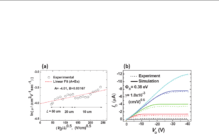
dependent mobility in TIPS-pentacene OTFTs is shown by extracting field-effect mobility of
devices with
L of 10, 20, and 50 μm at several values of V
DS
in linear region and plotted it as
a function of (
V
D
/L)
0.5
, as shown in Figure 3a (Cherian et al, 2004; Wang et al, 2003). The
logarithmic variation of mobility with (
V
D
/L)
0.5
for a series of channel lengths suggests that
it follows the Poole-Frenkel (PF)-type field-dependence given by:
()
exp
o
Fμ=μ γ (4)
where
μ
0
is the zero-field mobility, F is the electric field and γ is the characteristic parameter
for the field-dependence. A linear fit [dashed line in Fig. 4] to the data yielded field-
Numerical Simulations of Physical and Engineering Processes
84
dependent parameters of μ
o
= 0.035 cm
2
/Vs and γ =1.7×10
-3
(cm/V)
0.5
. It is noted that this PF
field-dependence is often observed in disordered organic semiconductors. In this respect,
the field-dependence of mobility given by Eq.4 is incorporated, in addition to the contact
barrier effect, into the numerical simulation. Line curves in Fig. 3b shows the simulated
output curves which take into account both the PF mobility and contact barriers. The best fit
to the experimental data was obtained with
Φ
B
of 0.38 eV, μ
o
of 0.061 cm
2
/Vs, and γ
of
1.8
×10
-3
(cm/V)
0.5
, respectively.
Fig. 3. (a) Natural logarithm of field-effect mobility as a function of (
V
D
/L)
0.5
. Dashed line is
a linear fit with which the field-dependent parameters are estimated to be
μ
o
= 0.035 cm
2
/Vs
and γ=1.7
×10
-3
(cm/V)
0.5
. (b) Output characteristics of TIPS-pentacene TFTs: experimental
(dotted) vs. numerical simulation (solid) results. Simulation was done in consideration of
both a contact barrier height Φ
B
of 0.38 eV, μ
o
= 0.061 cm
2
/Vs and γ=1.8×10
-3
(cm/V)
0.5
. V
G
is
varied from 0 to -40V in -10V steps. (Reprinted from
Organic Electronics, vol.9, D.Gupta, N.
Jeon, S. Yoo, “Modeling the electrical characteristics of TIPS-pentacene thin-film transistors:
Effect of contact barrier, field-dependent mobility, and traps”
, p.1026, 2008, with permission
from Elsevier)
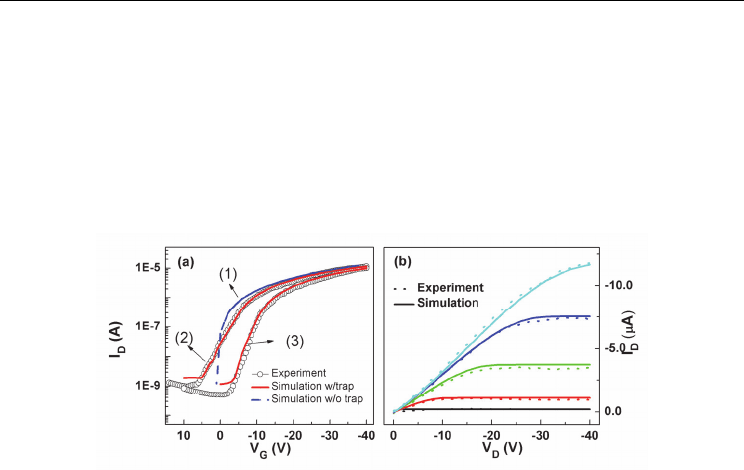
The incorporation of contact barrier and PF dependence of mobility show a reasonable
match to the output curves, but transfer curves still suffers from a significant deviation at
low |
V
G
| (curve 1 in Fig. 4a), which signifies include additional factors based on traps to
complete the TFT model. Moreover, a hysteresis loop in the
I
DS
-V
GS
transfer curve shown in
Fig. 4(a), when scanned
V
GS
from 0 to -40 V and then back from -40 to 0 V again indicate
about the existence of traps, which may come from dielectric-semiconductor interface or
from structural defects in TIPS-pentacene films (Alam et al, 1997; Scheinert et al, 2004).
This
trap-related phenomenon is simulated by assuming a spatially uniform density of trap
states in TIPS-pentacene films that is modeled by an exponential distribution of acceptor-
like traps as in Eq. 4a and 4b. It was previously discussed that oxygen is the chemical origin
of acceptor-like traps in pentacene and that acceptor-like traps provide extra hole current in
the subthreshold region in pentacene OTFTs (Alam et al, 1997; Knipp et al, 2003; Scheinert et
al, 2004; Street et al, 2002). Additionally, a positive interface trapped charge (
N
it
) is included,
which may arise due to impurities such as moisture, oxygen or mobile charges in the
dielectric. It was observed that the forward sweep (curve 2) can be better reproduced with
N
TA
= 1.0×10
18
cm
−3
eV
−1
, W
TA
= 0.55 eV and N
it
= 8.0×10
11
cm
−2
, while reverse sweep (curve
3) requires
N
TA
= 8.0×10
17
cm
−3
eV
−1
, W
TA
= 0.55 eV, N
it
= 2.0×10
12
cm
−2
, and μ
o
= 0.058
Importance of Simulation Studies in Analysis of Thin
Film Transistors Based on Organic and Metal Oxide Semiconductors
85
cm
2
/Vs. The increase in N
it
in the reverse sweep is a result of discharging of the trap states
that is relatively slow when compared to the sweep speed (= 5V/sec) used in this study and
is mainly responsible for the shift in threshold voltage. The output curves were also well
simulated with the additional incorporation of traps in TIPS- pentacene films, as shown in
Fig. 4b. Thus, this work is helpful in building an integral picture of injection, transport, and
traps in TIPS-pentacene in a context of OTFT operation, and will serve as a starting point for
further performance optimization and baseline for simulation of TFT made of any new
semiconductor.
Fig. 4. (a) Numerical fit to the transfer curves (curve 1 is without traps, while curves 2 and 3
are plotted using trap distribution given by Eq. 4 and interface charges in forward (2) and
reverse (3) bias sweep. (b) Output curves with DOS distribution and contact barrier height
of 0.38 eV, μ
o
= 0.052 cm
2
/Vs and γ=1.8×10
-3
(cm/V)
0.5
(Reprinted from Organic Electronics,
vol.9,
D.Gupta, N. Jeon, S. Yoo, “Modeling the electrical characteristics of TIPS-pentacene
thin-film transistors: Effect of contact barrier, field-dependent mobility, and traps”
, p.1026,
2008,
with permission from Elsevier)
4. Effect of device design of OTFT
In OTFTs, there is a common issue of difference in device performance of OTFTs fabricated
in top contact and bottom contact device configurations (Gundlach et al, 2006; Gupta et al
2009; Roichman et al, 2002; Street et al, 2002). The process difference between the two device
designs is that in top contact OTFT, semiconductor is deposited prior to depositing source
and drain electrodes, while this is vice versa in bottom contact OTFT. From fabrication point
of view, bottom contact OTFT is preferred because in this design the soft organic
semiconductor can be protected from harsh chemicals, high temperatures and metal
penetration. However, usually bottom contact OTFT show inferior performance, the reasons
for which is provided on the basis of large metal-semiconductor contact resistance, irregular
deposition or poor morphology of the semiconductor films around the source and drain
contacts (Kang et al, 2003; Kymissis et al, 2001; Koch et al, 2002; Lee et al 2006, Schroeder et
al, 2003). In the bottom contact OTFT, it is possible that both the contact barrier and the
structural inhomogenities in the semiconductor play important role in affecting the charge
injection and transport characteristics. However, separating one from the other and finding
the dominant role of one of the effects is necessary to properly understand the device
operation mechanisms.

Numerical Simulations of Physical and Engineering Processes
86
Fig. 5. (a) Schematic of the bottom contact device showing different region of pentacene
morphology. Scanning electron micrograph of pentacene on gold contact (b) near gold
contact edge on SiO
2
, (c) far away from gold contact edge on SiO
2
, (d) on gold contacts, and
(e) Schematic of the 1μm wide low-mobility-region near the source and drain contact edges
and above the contacts in bottom contact devices. (Reprinted from
Organic Electronics, Vol.
10, No. 1,
D. Gupta, M.Katiyar, Deepak, “An analysis of difference in device behavior of top
and bottom contact devices using device simulation”,
pp. 775-784, 2009, with permission from
Elsevier)
The experimental devices consist of n+ Si as gate, 40 nm gold as source and drain electrodes,
200 nm SiO
2
as gate insulator, and pentacene as the organic semiconductor. Pentacene films
with thicknesses of 50 nm are deposited by thermal evaporation at the rate of 0.03-0.04
nm/sec at substrate temperature of 65
o
C. The channel length (L) for both top and bottom
contact devices is 30 μm and their widths (W) are 1mm and 3.6mm, respectively. The
experimentally obtained data in the output curves were also corrected in order to remove
the effects of gate leakage and contact resistances (Gupta et al, 2009). To correct for the gate
leakage, half of the gate current is added to the obtained drain current at each gate voltage.
In order to correct the device characteristics for the metal-semiconductor contact resistance,
device parasitic resistance (R
P
) is calculated as a function of gate voltage following the
procedures provided in the well- known transmission line method (TLM). R
P
estimated by
TLM method is then used to correct the drain currents to their equivalent values in a device
with no metal-semiconductor contact resistance. From the as measured curves, the extracted
field effect mobility for top and bottom contact devices are 0.125 cm
2
/Vs and 1.74x10
-3
cm
2
/Vs, respectively, in the saturation region. After the gate leakage and contact resistance
correction, an effective mobility of 0.14 cm
2
/Vs and 3.2x10
-3
cm
2
/Vs is obtained for the top
and bottom contact devices, respectively.
The simulation data obtained from the top and bottom contact device structures overlay on
each other, which implies that device structure by itself is not responsible for causing any
difference in the two device structures. The other factors then must lay down to the
differences in the manner that two devices are fabricated. In bottom contact devices, it is
possible that a shadow cast by metal during evaporation of pentacene could lead to unfilled
corners at the source/drain contacts, which in turn could result in lower effective device
mobility. This kind of situation in the simulation is incorporated by adding a vacuum layer
of dimensions 50 nm x 40 nm adjacent to the source and drain electrodes. However, the
resultant drain currents are only slightly affected by the unfilled corners, as the current find
Importance of Simulation Studies in Analysis of Thin
Film Transistors Based on Organic and Metal Oxide Semiconductors
87
a way of charge injection/extraction through the top surface of the source and drain
electrodes, respectively. The next possibility, i.e. the effect of morphology of pentacene is
then deeply investigated in order to find out the reasons for inferior performance of bottom
contact devices. The investigation of pentacene morphology in the different regions of the
bottom contact device showed a marked variation in grain sizes. From the scanning electron
micrograph of the device in Fig. 5, one can clearly see that the large grain structure far away
from the source/drain contact edges changes into a small grain structure as one move closer
to the edge of the channel, near the gold electrodes. On SiO
2
, the average grain size is 0.57
μm and on the source and drain contacts, the grain size is 0.15 μm. The reason for such a
difference in morphology is attributed to the difference in surface energies of metal and
dielectric layers.
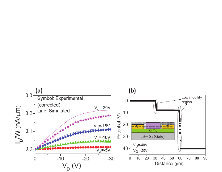
Fig. 6. (a) Comparison of the experimental (gate leakage and contact corrected) and the
simulated output curves. The mobility of the low-mobility-region is 1.5x10⁻⁴ cm
/#’
/Vs and
bulk mobility of pentacene is 0.14 cm
2
/Vs. (b) Surface potential profile 1 nm above the
dielectric surface (source, drain and channel lie between 0-30 μm, 60-90 μm and 30-60 μm,
respectively). (Reprinted from
Organic Electronics, Vol. 10, No. 1, D. Gupta, M.Katiyar,
Deepak
, “An analysis of difference in device behavior of top and bottom contact devices
using device simulation”,
pp. 775-784, 2009, with permission from Elsevier)
The above mentioned structural features are then incorporated in the simulation model (as
depicted in Fig. 5) where a low-mobility-region near the source and drain contact edges and
above the contacts is defined in the bottom contact device. The low-mobility-region has
lower mobility as compared to the rest of the pentancene, and the reason for such an
assignment is attributed to the significantly lower grain size as compared to the bulk film.
Keeping the bulk mobility as 0.14 cm
2
/Vs, several values of mobility of the low-mobility-
region are tried and a mobility value of 1.5x10
-4
cm
2
/Vs yields a good comparison with the
measured data, as shown in Fig. 6a. The effective mobility calculated from this structure is
1.8x10
-4
cm
2
/Vs, which closely matches with the experimental value. In order to analyze the
effects of low-mobility-region, potential profiles between the source and drain contacts at 1
nm above the dielectric interface (along a horizontal dashed line in the inset of Fig. 7b) are
taken. Figure 6b shows that almost all the applied potential is accommodated in the low-
mobility-region, forcing its effect on the overall device characteristics. The current density
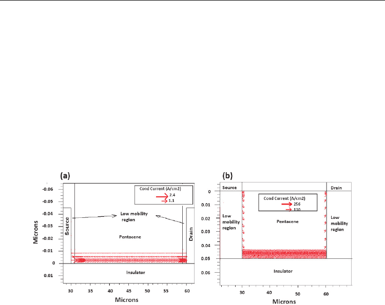
profiles (Fig. 7a) taken across the bottom contact device depicts that charge injection and
Numerical Simulations of Physical and Engineering Processes
88
extraction takes place from the lower region of metal contacts (within 5 nm region from the
insulator) forcing the current to pass through the low-mobility region and causing a large
potential drop. As an analogy, the low-mobility-region in the top contact devices is also
introduced below the source and drain electrodes, which spans across the full thickness of
pentacene. As an example, a mobility value of 1x10
-3
cm
2
/Vs for the low mobility region is
taken, but no significant change in the device behaviour could be observed. The reason for
this can be understood from the current density profile in Fig. 7b, which clearly indicates
that charge is injected from the side/corner of the contacts, bypassing the low-mobility-
region. Thus top contact devices would be less susceptible to morphological variations.
Therefore, the simulation determines that the possible cause of differences observed in
bottom and top contact devices could be due to differences in pentacene morphology
leading to low mobility regions near the contacts.
Fig. 7. Schematic diagram for the path of the current flow in pentacene film (line with the
arrow) in a (a) bottom contact device having a low-mobility region adjacent to and above the
source and drain contacts and in a (b) top contact device having a low-mobility-region
under the source and drain contacts. (Reprinted from
Organic Electronics, Vol. 10, No. 1, D.
Gupta, M.Katiyar, Deepak
, “An analysis of difference in device behavior of top and bottom
contact devices using device simulation”,
pp. 775-784, 2009, with permission from Elsevier)
5. Effect of pentacene thickness
The next issue of interest is dependence of device performance on the semiconductor
thickness. Theoretically, the device mobility should be independent of semiconductor
thickness in TFTs, because the field effect causes all the charges to be accumulated in few
nanometers of the semiconductor near the insulator, thus nullifying the effect of the rest of
the film (Dinelli et al, 2004; Horowitz et al 2003). However, practically, this is a common
observation and the reasons for such an occurrence are explained in terms of organic
semiconductor morphology, semiconductor-insulator interfaces, and access resistances
(Dodabalapur et al, 2005; Granstrom et al, 1999; Kiguchi et al, 2005; Schroeder et al 2003).
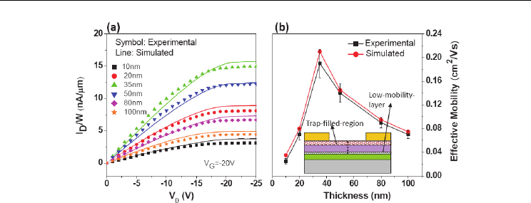
Figure 8 shows the mobility dependence of top contact OTFTs based on pentacene for
pentacene thicknesses of 10, 20, 35, 50, 80 and 100 nm, respectively. The source and drain
electrodes are made of gold, gate is n+ silicon, insulator is 200 nm thick SiO
2
, channel width
W is 1.5 mm and length L is 30 μm, respectively. According to the experiments, the mobility

Importance of Simulation Studies in Analysis of Thin
Film Transistors Based on Organic and Metal Oxide Semiconductors
89
increases until a pentacene thickness of 35 nm, and then it decreases. However, the
simulated device characteristics are only very slightly affected by pentacene thickness (Fig.
8a), and not to the extent of experimental observations. Since there is a sufficient mobility
variation with pentacene thickness experimentally, it is imperative to incorporate
additional features in the simulation in order to model the device characteristics
accurately. In the simulation, the physical behavior related to charge transport in the first
few layers adjacent to the dielectric is not modeled. However, it is important to note that
the first few layers, where most of the charge transport occurs, may have different
electronic properties as compared to the bulk film. In literature, it has been demonstrated
that the pentacene film near the dielectric may have several structural defects,
discontinuities, low surface coverage and may also be affected by charge-surface phonon
interaction caused by the polar oxide dielectric (Houilli et al 2006; Kiroval et al, 2003;
Puntambekar et al, 2005; Sandberg et al, 2002; Stassen et al, 2004; Steudel et al, 2004; Ruiz
et al 2005; Veres et al, 2002). Apart from this, inter layer surface potential between the
pentacene layers and polarization interaction energy of the charge in the dielectric may
force the mobile carriers more towards the vicinity of the dielectric (Houilli et al 2006;
Kiroval et al, 2003; Puntambekar et al, 2005). Based on this discussion, following two
points emerge (Gupta et al, 2009):
a.
A monolayer of pentacene may have low mobility in comparison to the bulk pentacene.
Hereafter this layer is referred as low mobility layer.
b.
Mobile charge, for reasons not precisely understood, is preferentially forced to this low
mobility region.
These effects are then systematically introduced in the simulation model for a better match
with the experimental data. To evaluate the effect of the low mobility layer at the insulator
surface, 1.5 nm thick layer (roughly the thickness of a monolayer of pentacene) at the
dielectric interface is incorporated, as depicted in the inset of Fig. 8b. The simulations were
performed while keeping the bulk mobility value of 0.28 cm
2
/Vs, and lowering the mobility
of the low-mobility-layer down to several decades. However, the extracted mobility from
the simulation increases until pentacene thickness of 35 nm and then becomes almost
constant (Fig. 8b ). This simulated behaviour is significantly different than the experimental
results and thus the second effect, ie charge confinement towards dielectric is investigated
subsequently.
Since the commercial simulator in use here does not contain any models to physically
simulate the carrier confinement, an energy band offset between the low mobility layer and
bulk pentacene is intentionally introduced in the simulation model in such a way that it
facilitates the charge migration towards the low mobility layer. Figure 9a shows the energy
band diagram of pentacene film depicting the energy band offset between the low mobility
layer and the bulk pentacene. To force the mobile charge towards the low mobility layer, the
electron affinity (E
A
) value of the low mobility layer (E
A1
) is reduced in comparison to its
value in the bulk pentacene (E
A2
), while keeping the band gap (E
g
) value same for both the
regions. The combined effect of low-mobility-layer and the charge confinement induced by
the above mentioned method is such that the effective mobility of the device reduces
significantly as compared to the bulk mobility value. For example, for a pentacene thickness
of 50nm, a bulk mobility value of 0.28 cm
2
/Vs, a low-mobility-value of 0.014 cm
2
/Vs and an
energy band-offset of 0.1 eV produce an effective mobility value of 0.09 cm
2
/Vs. With
several trials and errors, it was observed that the quantitative behavior of mobility up to 35

Numerical Simulations of Physical and Engineering Processes
90
nm is better matched for an energy band offset value of 0.11 eV, the mobility of low mobility
layer as ~1x10
-4
cm
2
/Vs and bulk mobility as 1.3 cm
2
/Vs (Fig. 9b). However, as shown in
Fig. 9b, after 35 nm, no match could be obtained, which is discussed based on the pentacene
morphology variation with thickness, in the next paragraph.
Fig. 8. (a) A comparison of the mobility values for the experimental and the simulated
devices and (b) between experimental and simulated devices on incorporating the low-
mobility-layer as a function of pentacene thickness. (Reprinted from
Organic Electronics, Vol.
11, D. Gupta, Y. Hong, “Understanding the effect of semiconductor thickness on
device characteristics in organic thin film transistors by way of two dimensional
simulations
”, pp. 127-136, 2010, with permission from Elsevier)
Fig. 9. (a) Schematic diagram of the energy levels in the low mobility layer and bulk of the
pentacene film (b) Comparison of experimental and simulated mobility value as a function
of pentacene thickness. The mobility of the low-mobility-layer is 1x10
-4
cm
2
/Vs and bulk
mobility is 1.3 cm
2
/Vs. The energy band offset value is 0.11 eV. (Reprinted from Organic
Electronics,
Vol. 11, D. Gupta, Y. Hong, “Understanding the effect of semiconductor
thickness on device characteristics in organic thin film transistors by way of two
dimensional simulations”,
pp. 127-136, 2010, with permission from Elsevier)
Importance of Simulation Studies in Analysis of Thin
Film Transistors Based on Organic and Metal Oxide Semiconductors
91
Fig. 10. A comparison of simulated and experimental (a) output curves and (b) mobility
value as a function of pentacene thickness. The mobility of the low-mobility-layer and bulk
pentacene is taken as 1x10
-4
cm
2
/Vs and 1.3 cm
2
/Vs, respectively. The energy band offset
value is 0.11 eV. The trap concentration is taken as 4x10
16
cm
-3
for 50 nm thick film and
6x10
16
cm
-3
for 80 and 100 nm thick films, respectively. (Reprinted from Organic Electronics,
Vol. 11, D. Gupta, Y. Hong, “Understanding the effect of semiconductor thickness on device
characteristics in organic thin film transistors by way of two dimensional simulations”,
pp.
127-136, 2010, with permission from Elsevier)
The investigation of morphology of pentacene films revealed that grain size and crystal
structure varies as a function of thickness. It is found that until pentacene thickness of 35
nm, the average grain size remains ~0.85 μm. After further increasing the film thickness, the
grain size reduces and reaches to 0.15 μm for the 100 nm thick pentacene films. The
reduction in grain size causes more grain boundaries to appear, which acts as trapping
centers for the mobile charge. The bulk traps in the region above 35 nm of pentacene
thickness are then introduced, as illustrated in the inset of Fig. 10b. It was found that the
donor type traps with a trap level of 0.4eV, produces a reasonable match between the
experimental and simulated curves, if bulk donor trap concentration of 4x10
16
cm
-3
for 50 nm
thick film and 6x10
16
cm
-3
for 80 and 100 nm thick films, respectively, are chosen. Figure 10a
and 10b show the superimposed experimental and simulated results of the output curves
and mobility values, respectively. Therefore, this study indicates that OTFT devices face
several non-regularities, which are expressed in the form of low-mobility of the pentacene
layers that are associated with the dielectric, existence of energy band offset between the
interface layers and the bulk, and the bulk traps due to the structural defects like grain
boundaries. The combined effect of these features causes the extracted mobility to depend
on the film thickness, which in an ideal case should have been absent. It also signifies the
importance of optimizing the thickness of organic semiconductor in order to have enhanced
as well as reliable device performance.
6. Device stability of solution processed ZnO TFTs under electrical stress
Device stability of TFTs under electrical stress is highly important in view of practicality,
which is not only important in estimating the device lifetime but also in understanding the
instability mechanisms. Electrical instability in TFTs is typically measured by threshold
voltage (V
T
) shift that occurs when the device is subjected to constant voltage or drain current
Numerical Simulations of Physical and Engineering Processes
92
for certain duration (Wehrspon et 2003, Jahinuzzaman et al, 2005). During constant gate bias,
the channel charge and hence the on current continuously decreases to eventually saturate the
V
T
shift. On the other hand, during constant current stress the applied gate bias continually
adjusts itself in time to keep the drain current constant. Also important is the post-stress
relaxation characteristics of the device, where V
T
shift occurring during the stress state is
recovered in the off-state. From a practical point of view, this situation occurs in displays or
integrated circuits where the device is temporarily switched on, and then switched off.
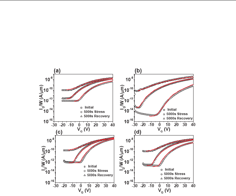
Fig. 11. Measured (symbol) and simulated (line) transfer characteristics showing initial
curve, after stressing for 5000 sec and after relaxation for 5000 sec for stress values of (a) 20 V
of gate bias, (b) 50 V of gate bias and (c) 5x10
-6
A of drain current and (d) 3x10
-5
A of drain
current.
The ZnO-TFT is fabricated in a simple bottom-gate top-contact configuration. In this device,
n++ silicon wafer served as gate electrode, Al as source and drain electrode, 100 nm-thick
SiO
2
film as gate insulator onto which sol-gel processed ZnO films are spin-coated. The sol is
prepared by making a 0.5 M solution of zinc acetate in the solvent mixture of DMF and
methoxy-ethanol (volume ratio=3:2) (Gupta et al, 2008) and then spin-coated twice on the
wafer. The films were pyrolyzed at 500
o
C for 1 hour, yielding polycrystalline films with an
average grain size of 300 nm. The channel width is 1.0 mm and channel length is 50 μm,
respectively. During electrical stress measurements in bias stress mode, a voltage is applied
only to the gate while keeping the source and drain grounded in order to create a uniform
electric field across the channel interface. During the current stressing, a constant current
was applied to the drain keeping the gate and drain connected in a diode-connected
configuration, while keeping the source grounded. This measurement configuration allows
automatic adjustment of the gate/drain to source voltage (V
GS
=V
DS
) to achieve a constant
drain current. The relaxation characteristics are measured soon after the stressing period of
5000 sec, while keeping all three terminals grounded. Figure 11a – 11d shows the obtained
