Bichop R.H. (Ed.) Mechatronic Systems, Sensors, and Actuators: Fundamentals and Modeling
Подождите немного. Документ загружается.

15-4 Mechatronic Systems, Sensors, and Actuators
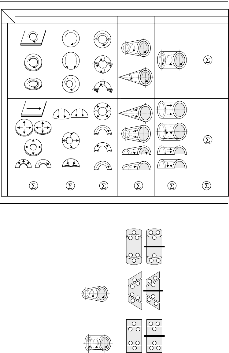
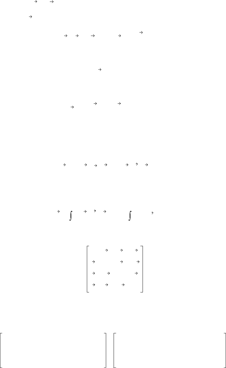
TABLE 15.1 Classification of Electromagnetic Microdevices Using the Electromagnetic
System–Geometry Classifier
FIGURE 15.1 Permanent-magnet synchronous micromachines with different geometry.
Geometry
Plate, P Spherical, S Torroidal, T Conical, N Cylindrical, C
Endless (closed), E
Open-Ended
(open),
O
Asymmetrical, A
M
G
Integrated,
I
Electromagnetic system
Endless electromagnetic system
and cylindrical geometry
Endless electromagnetic system
and conical geometry
Endless electromagnetic system
and spherical geometry
Stator
Rotor
S
N
Rotor
Stator
N
S
as
bs
as
bs
Rotor
Stator
as
bs
Rotor
N
S
N
S
as
bs
Rotor
Stator
Stator
as
bs
Rotor
N
N
S
S
as
bs
as
bs
as
bs
as
bs
as
bs
as
bs
as
bs
Stator
9258_C015.fm Page 4 Tuesday, October 2, 2007 3:35 AM
Rotational and Translational Microelectromechanical Systems 15-5
into three horizontal and six vertical strips, and contains 18 sections, each identified by ordered pairs of
characters, such as (E, P) or (O, C).
In each ordered pair, the first entry is a letter chosen from the bounded electromagnetic system set
The second entry is a letter chosen from the geometric set
That is, for electromagnetic microdevices, the electromagnetic system–geometric set is
In general, we have
Other categorization can be applied. For example, single-, two-, three-, and multi-phase microdevices
are classified using a phase classifier
Therefore, Y × M × G × H = {(y, m, g, h) : y ∈ Y, m ∈ M, g ∈ G and h ∈ H}
Topology (radial or axial), permanent magnets shaping (strip, arc, disk, rectangular, triangular, or
other shapes), permanent magnet characteristics (BH demagnetization curve, energy product, hysterisis
minor loop), commutation, emf distribution, cooling, power, torque, size, torque-speed characteristics,
as well as other distinct features of microdevices can be easily classified.
That is, the devised electromagnetic microdevices can be classified by an N-tuple as
{microdevice type, electromagnetic system, geometry, topology, phase, winding, connection, cooling}.
Using the classifier, which is given in Table 15.1 in terms of electromagnetic system–geometry, the
designer can classify the existing motion microdevices as well as synthesize novel high-performance
microdevices. As an example, the spherical, conical, and cylindrical geometries of a two-phase permanent-
magnet synchronous microdevice are illustrated in Figure 15.2.
This section documents new results in structural synthesis which can be used to optimize the microde-
vice performance. The conical (existing) and spherical-conical (devised) microdevice geometries are
illustrated in Figure 15.2. Using the innovative spherical-conical geometry, which is different compared
to the existing conical geometry, one increases the active length L
r
and average diameter D
r
. For radial
flux microdevices, the electromagnetic torque T
e
is proportional to the squared rotor diameter and axial
length. In particular, where k
T
is the constant. From the above relationship, it is evident
FIGURE 15.2 Two-phase permanent-magnet synchronous microdevice (micromachine) geometry.
ME, O, I{}=
GP, S, T, N, C, A{}=
MG× E, F(), E, S(), E, T(),…, I, N(), I, C(), I, A(){}=
MG× m, g():mM and ∈ gG∈{}=
Hh: hH∈{}=
T
e
k
T
D
r
2
L
r
,=
Cylindrical geometry
Rotor
Stator
Rotor
Stator
Stator
as
bs
Rotor
Stator
Rotor
S
N
Rotor
Stator
Conical geometry
Spherical geometry
Stator
as
bs
Rotor
N
S
N
S
N
S
Stato
r
Rotor
S
N
Stator
Stato
r
Rotor
S
bs
as
N
Stator
N
N
S
S
Spherical-conical
geometry
Endless electromagnetic system
Assymetrical geometr
y
Stator
Roto
r
S
N
Rotor
S
N
Rotor
Stator
Stator
as
bs
as
bs
as
bs
as
bs
as
bs
as
b
s
as
bs
9258_C015.fm Page 5 Tuesday, October 2, 2007 3:35 AM

15-6 Mechatronic Systems, Sensors, and Actuators
that the spherical-conical micromotors develop higher electromagnetic torque compared with the con-
ventional design. In addition, improved cooling, reduced undesirable torques components, as well as
increased ruggedness and robustness contribute to the viability of the proposed solution. Thus, using
the classifier paradigm, novel microdevices with superior performance can be devised.
15.3 MEMS Fabrication
Microelectromechanics, which integrates micromechanics and microelectronics, requires affordable, low-
cost, high-yield fabrication technologies which allow one to fabricate 3-D microscale structures and
devices. Micromachining is a key fabrication technology for microscale structures, devices, and MEMS.
Microelectromechanical systems fabrication technologies fall into three broad categories: bulk machining,
surface machining, and LIGA (LIGA-like) techniques [1–3].
15.3.1 Bulk Micromachining
Bulk and surface micromachining are based on the modified CMOS and specifically designed microma-
chining processes. Bulk micromachining of silicon uses wet and dry etching techniques in conjunction
with etch masks and etch-stop-layers to develop microstructures from the silicon substrate. Microstruc-
tures are fabricated by etching areas of the silicon substrate to release the desired 3-D microstructures.
The anisotropic and isotropic wet etching processes, as well as concentration dependent etching techniques,
are widely used in bulk micromachining. The microstructures are formed by etching away the bulk of
the silicon wafer to fabricate the desired 3-D structures. Bulk machining with its crystallographic and
dopant-dependent etch processes, when combined with wafer-to-wafer bonding, produces complex 3-D
microstructures with the desired geometry. Through bulk micromachining, one fabricates microstruc-
tures by etching deeply into the silicon wafer. There are several ways to etch the silicon wafer. The
anisotropic etching uses etchants that etch different crystallographic directions at different rates. Through
anisotropic etching, 3-D structures (cons, pyramids, cubes, and channels into the surface of the silicon
wafer) are fabricated. In contrast, the isotropic etching etches all directions in the silicon wafer at same
(or close) rate, and, therefore, hemisphere and cylinder structures can be made. Deep reactive ion etching
uses plasma to etch straight walled structures (cubes, rectangular, triangular, etc.).
15.3.2 Surface Micromachining
Surface micromachining has become the major fabrication technology in recent years because complex
3-D microscale structures and devices can be fabricated. Surface micromachining with single-crystal
silicon, polysilicon, silicon nitride, silicon oxide, and silicon dioxide (as structural and sacrificial materials
which deposited and etched) is widely used to fabricate microscale structures and devices on the surface
of a silicon wafer. This affordable low-cost high-yield technology is integrated with IC fabrication
processes guaranteeing the needed microstructures-IC fabrication compatibility. The techniques for
depositing and patterning thin films are used to produce complex microstructures and microdevices on
the surface of silicon wafers (surface silicon micromachining) or on the surface of other substrates. Surface
micromachining technology allows one to fabricate the structure as layers of thin films. This technology
guarantees the fabrication of 3-D microdevices with high accuracy, and the surface micromachining can
be called a thin film process. Each thin film is usually limited to thickness up to 5
µ
m, which leads to
fabrication of high-performance planar-type microscale structures and devices. The advantage of surface
micromachining is the use of standard CMOS fabrication processes and facilities, as well as compliance
with ICs. Therefore, this technology is widely used to manufacture microscale actuators and sensors
(microdevices).
Surface micromachining is based on the application of sacrificial (temporary) layers that are used to
maintain subsequent layers and are removed to reveal (release) fabricated (released or suspended) micro-
structures. This technology was first demonstrated for ICs and applied to fabricate microstructures in
the 80s. On the surface of a silicon wafer, thin layers of structural and sacrificial materials are deposited
9258_C015.fm Page 6 Tuesday, October 2, 2007 3:35 AM
Rotational and Translational Microelectromechanical Systems 15-7
and patterned. Then, the sacrificial material is removed, and a micromechanical structure or device is
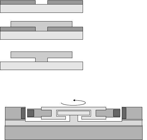
fabricated. Figure 15.3 illustrates a typical process sequence of the surface micromachining fabrication
technology.
Usually, the sacrificial layer is made of silicon dioxide (SiO
2
), phosphorous-doped silicon dioxide, or
silicon nitride (Si
3
N
4
). The structural layers are then typically formed with polysilicon, and the sacrificial
layer is removed. In particular, after fabrication of the surface microstructures and microdevices (micro-
machines), the silicon wafer can be wet bulk etched to form cavities below the surface components, which
allows a wider range of desired motion for the device. The wet etching can be done using hydrofluoric
and buffered hydrofluoric acids, potassium hydroxide, ethylene-diamene-pyrocatecol, tetramethylam-
monium hydroxide, or sodium hydroxide. Surface micromachining technology was used to fabricate
rotational micromachines [6]. For example, heavily-phosphorous-doped polysilicon can be used to
fabricate rotors and stators, and silicon nitride can be applied as the structural material to attain electrical
insulation. The cross-section of the slotless micromotor fabricated on the silicon substrate with polysilicon
stator with deposited windings, polysilicon rotor with deposited permanent-magnets, and bearing is
illustrated in Figure 15.4. The micromotor is controlled by the driving/sensing and controlling/processing
ICs. To fabricate micromotor and ICs on a single- or double-sided chip (which significantly enhances
the performance), similar fabrication technologies and processes are used, and the compatibility issues
are addressed and resolved. The surface micromachining processes were integrated with the CMOS
technology (e.g., similar materials, lithography, etching, and other techniques). To fabricate the integrated
MEMS, post-, mixed-, and pre-CMOS/micromachining techniques can be applied [1–3].
15.3.3 LIGA and LIGA-Like Technologies
There is a critical need to develop the fabrication technologies allowing one to fabricate high-aspect-
ratio microstructures. The LIGA process, which denotes Lithography–Galvanoforming–Molding (in
German words, Lithografie–Galvanik–Abformung), is capable of producing 3-D microstructures of up
to centimeter high with the aspect ratio (depth versus lateral dimension) more than 100 [2,7,8]. The
LIGA technology is based upon X-ray lithography, which guarantees shorter wavelength (in order from
FIGURE 15.3 Surface micromachining.
FIGURE 15.4 Cross-section schematics for slotless permanent-magnet brushless micromotor with ICs.
1. Deposition and patterning
of the sacrificial layer
Silicon substrate
Sacrificial layer
Sacrificial layer
2. Deposition and patterning
of the structural layer
Silicon substrate
Sacrificial layerSacrificial layer
Structural layer
3. Etching of the sacrificial
layer
Structural layer
Silicon substrate
Micromachined structure
Silicon substrate
Stator
Rotor
Bearing post
Bearing flange
Permanent
magnet
Stator
windings
Rotor
Stator
r
Insulating
Insulating
ICs
ω
9258_C015.fm Page 7 Tuesday, October 2, 2007 3:35 AM

15-8 Mechatronic Systems, Sensors, and Actuators
few to 10 Å, which leads to negligible diffraction effects) and larger depth of focus compared with optical
lithography. The ability to fabricate microstructures and microdevices in the centimeter range is partic-
ularly important in the actuators and drives applications since the specifications are imposed on the
rated force and torque developed by the microdevices, and due to the limited force and torque densities,
the designer faces the need to increase the actuator dimensions.
15.4 MEMS Electromagnetic Fundamentals and Modeling
The MEMS classifier, structural synthesis, and optimization were reported in Section 15.2. The classifica-
tion and optimization are based on the consideration and synthesis of the electromagnetic system, analysis
of the magnetomotive force, design of the MEMS geometry and topology, and optimization of other
quantities. Different rotational (radial and axial) and translational motion microdevices are classified
using endless (closed), open-ended (open), and integrated electromagnetic systems.
Our goal is to approach and solve a wide range of practical problems encountered in nonlinear design,
modeling, analysis, control, and optimization of motion microstructures and microdevices with driving/
sensing circuitry controlled by ICs for high-performance MEMS. Studying MEMS, the emphases are
placed on:
•
Design of high-performance MEMS through devising innovative motion microdevices with radi-
ating energy microdevices, microscale driving/sensing circuitry, and controlling/signal processing
ICs
•
Optimization and analysis of rotational and translation motion microdevices
•
Development of high-performance signal processing and controlling ICs for microdevices devised
•
Development of mathematical models with minimum level of simplifications and assumptions in
the time domain
•
Design of optimal robust control algorithms
•
Design of intelligent systems through self-adaptation, self-organization, evolutionary learning,
decision-making, and intelligence
•
Development of advanced software and hardware to attain the highest degree of intelligence,
integration, efficiency, and performance
In this section, our goal is to perform nonlinear modeling, analysis, and simulation. To attain these
objectives, we apply the MEMS synthesis paradigm, develop nonlinear mathematical models to model
complex electromagnetic-mechanical dynamics, perform optimization, design closed-loop control sys-
tems, and perform data-intensive analysis in the time domain.
To model electromagnetic motion microdevices, using the magnetic vector and electric scalar potentials
and V, respectively, one usually solves the partial differential equations
using finite element analysis. Here,
µ
,
σ
, and
ε
are the permeability, conductivity, and permittivity.
However, to design electromagnetic MEMS as well as to perform electromagnetic–mechanical analysis
and optimization, differential equations must be solved in the time domain. In fact, basic phenomena
cannot be comprehensively modeled, analyzed, and assessed applying traditional finite element analysis,
which gives the steady-state solutions and models. There is a critical need to develop the modeling tools
that will allow one to augment nonlinear electromagnetics and mechanics in a single electromagnetic–
mechanical modeling core to attain high-fidelity analysis with performance assessment and outcome
prediction.
Operating principles of MEMS are based upon electromagnetic principles. A complete electromagnetic
model is derived in terms of five electromagnetic field vectors. In particular, three electric field vectors
A
∇
2
– A
µσ
+
∂
A
∂
t
-------
µε
+
∂
2
A
∂
t
2
---------
µσ
∇V–=
9258_C015.fm Page 8 Tuesday, October 2, 2007 3:35 AM
Rotational and Translational Microelectromechanical Systems 15-9
and two magnetic field vectors are used. The electric field vectors are the electric field intensity, , the
electric flux density, , and the current density, . The magnetic field vectors are the magnetic field
intensity and the magnetic field density . The differential equations for microelectromechanical
motion device are found using Maxwell’s equations, constitutive (auxiliary) equations, and classical
mechanics.
Maxwell’s partial differential equations in the - and -domain in the point form are
where
ε
is the permittivity,
µ
is the permeability,
σ
is the conductivity, and
ρ
v
is the volume charge density.
The constitutive (auxiliary) equations are given using the permittivity
ε
, permeability tensor
µ
, and
conductivity
σ
. In particular, one has
The Maxwell’s equations can be solved using the boundary conditions on the field vectors. In two-
region media, we have
where is the surface current density vector, is the surface normal unit vector at the boundary from
region 2 into region 1, and is the surface charge density.
The constitutive relations that describe media can be integrated with Maxwell’s equations, which relate
the fields in order to find two partial differential equations. Using the electric and magnetic field intensities
and to model electromagnetic fields in MEMS, one has
The following pair of homogeneous and inhomogeneous wave equations
E
D
J
H
B
E
H
∇ Ex, yzt,,()×
µ
∂
Hx, yzt,,()
∂
t
-------------------------------
–=
∇ Hx, yzt,,()×
ε
∂
Ex, yzt,,()
∂
t
------------------------------
Jx, yzt,,()+
ε
∂
Ex, yzt,,()
∂
t
------------------------------
σ
Ex, yzt,,()+==
∇ Ex, yzt,,()⋅
ρ
v
x, yzt,,()
ε
-----------------------------
=
∇ Hx, yzt,,()⋅ 0=
D
ε
E or D
ε
EP+==
B
µ
H or B
µ
HM+()==
J
σ
E or J
ρ
ν
v
==
a
N
E
2
E
1
–()× 0, = a
N
H
2
H
1
–()× J
s
,
= a
N
D
2
D
1
–()⋅
ρ
s
,= a
N
B
2
B
1
–()⋅ 0=
J
s
a
N
ρ
s
E
H
∇∇E×()×∇∇E⋅()∇
2
– E −
µ
∂
J
∂
t
------
µ
∂
2
D
∂
t
2
----------
–
µσ
∂
E
∂
t
------
–
µε
∂
2
E
∂
t
2
---------
–===
∇∇H×()×∇∇H⋅()∇
2
– H
µσ
∂
H
∂
t
-------
–
µε
∂
2
H
∂
t
2
----------
–==
∇
2
E
µσ
∂
E
∂
t
------
–
µε
∂
2
E
∂
t
2
---------
– ∇
ρ
v
ε
-----
=
∇
2
H
µσ
∂
H
∂
t
-------
–
µε
∂
2
H
∂
t
2
----------
– 0=
9258_C015.fm Page 9 Tuesday, October 2, 2007 3:35 AM
15-10 Mechatronic Systems, Sensors, and Actuators
is equivalent to four Maxwell’s equations and constitutive relations. For some cases, these two equations
can be solved independently. It must be emphasized that it is not always possible to use the boundary
conditions using only and , and thus, the problem not always can be simplified to two electromagnetic
field vectors. Therefore, the electric scalar and magnetic vector potentials are used. Denoting the magnetic
vector potential as and the electric scalar potential as V, we have
The electromagnetic field is derivative from the potentials. Using the Lorentz equation
the inhomogeneous vector potential wave equation to be solved is
To model motion microdevices, the mechanical equations must be used, and Newton’s second law is
usually applied to derive the equations of motion.
Using the volume charge density
ρ
v
, the Lorenz force, which relates the electromagnetic and mechanical
phenomena, is found as
The electromagnetic force can be found by applying the Maxwell stress tensor method. This concept
employs a volume integral to obtain the stored energy, and stress at all points of a bounding surface can
be determined. The sum of local stresses gives the net force. In particular, the electromagnetic stress is
The electromagnetic stress energy tensor (the second Maxwell stress tensor) is
In general, the electromagnetic torque developed by motion microstructures is found using the elec-
tromagnetic field. In particular, the electromagnetic stress tensor is given as
E
H
A
∇ A× B
µ
H== and E
∂
A
∂
t
-------– ∇V–=
∇ A⋅
∂
V
∂
t
-------–=
∇
2
– A
µσ
∂
A
∂
t
-------
µε
∂
2
A
∂
t
2
---------
++
µσ
∇V–=
F
ρ
v
Ev+ B×()
ρ
v
EJB×+==
F
ρ
ν
EJ+ B×()vd
v
1
µ
---
T
αβ
↔
ds⋅
s
°
==
T
αβ
↔
0 E
x
E
y
E
z
E
x
– 0 B
z
B
y
–
E
y
– B
z
– 0 B
x
E
z
– B
y
B
x
– 0
=
T
s
T
s
E
T
s
M
+=
E
1
D
1
1
2
--
E
j
D
j
– E
1
D
2
E
1
D
3
E
2
D
1
E
2
D
2
1
2
--
E
j
D
j
– E
2
D
3
E
3
D
1
E
3
D
2
E
3
D
3
1
2
--
E
j
D
j
–
B
1
H
1
1
2
--
B
j
H
j
– B
1
H
2
B
1
H
3
B
2
H
1
B
2
H
2
1
2
--
B
j
H
j
– B
2
H
3
B
3
H
1
B
3
H
2
B
3
H
3
1
2
--
B
j
H
j
–
+=
9258_C015.fm Page 10 Tuesday, October 2, 2007 3:35 AM
Rotational and Translational Microelectromechanical Systems 15-11
For the Cartesian, cylindrical, and spherical coordinate systems, which can be used to develop the
mathematical model, we have
Maxwell’s equations can be solved using the M
ATLAB environment.
In motion microdevices, the designer analyzes the torque or force production mechanisms.
Newton’s second law for rotational and translational motions is
where
ω
r
and
θ
r
are the angular velocity and displacement, v and x are the linear velocity and displacement,
is the net torque, is the net force, J is the equivalent moment of inertia, and m is the mass.
15.5 MEMS Mathematical Models
The problems of modeling and control of MEMS are very important in many applications. A mathe-
matical model is a mathematical description (in the form of functions or equations) of MEMS, which
integrate motion microdevices (microscale actuators and sensors), radiating energy microdevices, micro-
scale driving/sensing circuitry, and controlling/signal processing ICs. The purpose of the model devel-
opment is to understand and comprehend the phenomena, as well as to analyze the end-to-end behavior.
To model MEMS, advanced analysis methods are required to accurately cope with the involved highly
complex physical phenomena, effects, and processes. The need for high-fidelity analysis, computationally-
efficient algorithms, and simulation time reduction increases significantly for complex microdevices, restrict-
ing the application of Maxwell’s equations to problems possible to solve. As was illustrated in the previous
section, nonlinear electromagnetic and energy conversion phenomena are described by the partial differ-
ential equations. The application of Maxwell’s equations fulfills the need for data-intensive analysis capa-
bilities with outcome prediction within overall modeling domains as particularly necessary for simulation
and analysis of high-performance MEMS. In addition, other modeling and analysis methods are applied.
The lumped mathematical models, described by ordinary differential equations, can be used. The process
of mathematical modeling and model development is given below.
The first step is to formulate the modeling problem:
•
Examine and analyze MEMS using a multilevel hierarchy concept, develop multivariable input-
output subsystem pairs, for example, motion microstructures (microscale actuators and sensors),
radiating energy microdevices, microscale circuitry, ICs, controller, input/output devices.
•
Understand and comprehend the MEMS structure and system configuration.
•
Gather the data and information.
•
Develop input-output variable pairs, identify the independent and dependent control, disturbance,
output, reference (command), state and performance variables, as well as events.
E
x
E
1
= , E
y
E
2
, E
z
E
3
,==D
x
D
1
= , D
y
D
2
, D
z
D
3
,==
H
x
H
1
= , H
y
H
2
, H
z
H
3
,==B
x
B
1
= , B
y
B
2
, B
z
B
3
==
E
r
E
1
= , E
θ
E
2
, E
z
E
3
,==D
r
D
1
= , D
θ
D
2
, D
z
D
3
,==
H
r
H
1
= , H
θ
H
2
, H
z
H
3
,==B
r
B
1
= , B
θ
B
2
, B
z
B
3
==
E
ρ
E
1
= , E
θ
E
2
, E
φ
E
3
,==D
ρ
D
1
= , D
θ
D
2
, D
φ
D
3
,==
H
ρ
H
1
= , H
θ
H
2
, H
φ
H
3
,==B
ρ
B
1
= , B
θ
B
2
, B
φ
B
3
==
d
ω
r
dt
---------
1
J
--
T
Σ
,=
d
θ
r
dt
--------
ω
r
=
dv
dt
-----
1
m
----
F
Σ
,=
dx
dt
------
v=
T
Σ
F
Σ
9258_C015.fm Page 11 Tuesday, October 2, 2007 3:35 AM
15-12 Mechatronic Systems, Sensors, and Actuators
•
Making accurate assumptions, simplify the problem to make the studied MEMS mathematically
tractable (mathematical models, which are the idealization of physical phenomena, are never
absolutely accurate, and comprehensive mathematical models simplify the reality to allow the
designer to perform a thorough analysis and make accurate predictions of the system performance).
The second step is to derive equations that relate the variables and events:
•
Define and specify the basic laws (Kirchhoff, Lagrange, Maxwell, Newton, and others) to be used
to obtain the equations of motion. Mathematical models of electromagnetic, electronic, and
mechanical microscale subsystems can be found and augmented to derive mathematical models
of MEMS using defined variables and events.
•
Derive mathematical models.
The third step is the simulation, analysis, and validation:
•
Identify the numerical and analytic methods to be used in analysis and simulations.
•
Analytically and/or numerically solve the mathematical equations (e.g., differential or difference
equations, nonlinear equations, etc.).
•
Using information variables (measured or observed) and events, synthesize the fitting and mis-
match functionals.
•
Verify the results through the comprehensive comparison of the solution (model input-state-
output-event mapping sets) with the experimental data (experimental input-state-output-event
mapping sets).
•
Calculate the fitting and mismatch functionals.
•
Examine the analytical and numerical data against new experimental data and evidence.
If the matching with the desired accuracy is not guaranteed, the mathematical model of MEMS must be
refined, and the designer must start the cycle again.
Electromagnetic theory and classical mechanics form the basis for the development of mathematical
models of MEMS. It was illustrated that MEMS can be modeled using Maxwell’s equations and torsional-
mechanical equations of motion. However, from modeling, analysis, design, control, and simulation
perspectives, the mathematical models as given by ordinary differential equations can be derived and used.
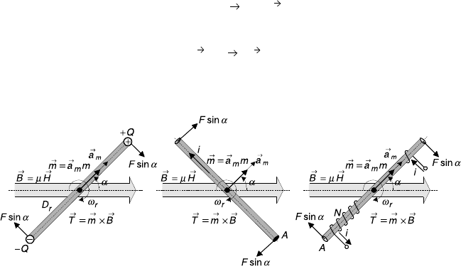
Consider the rotational microstructure (bar magnet, current loop, and microsolenoid) in a uniform
magnetic field, see Figure 15.5. The microstructure rotates if the electromagnetic torque is developed.
The electromagnetic field must be studied to find the electromagnetic torque.
The torque tends to align the magnetic moment with and
FIGURE 15.5 Clockwise rotation of the motion microstructure.
m B,
TmB×=
9258_C015.fm Page 12 Tuesday, October 2, 2007 3:35 AM
Rotational and Translational Microelectromechanical Systems 15-13
For a microstructure with outside diameter D
r
, the magnet strength is Q. Hence, the magnetic moment
is m = QD
r
, and the force is found as F = QB.
The electromagnetic torque is
Using the unit vector in the magnetic moment direction one obtains
For a current loop with the area A, the torque is found as
For a solenoid with N turns, one obtains
As the electromagnetic torque is found, using Newton’s second law, one has
where is the load torque.
The electromotive (emf ) and magnetomotive (mmf ) forces can be used in the model development.
We have
and
For preliminary design, it is sufficiently accurate to apply Faraday’s or Lenz’s laws, which give the
electromotive force in term of the time-varying magnetic field changes. In particular,
where is the transformer term.
The total flux linkages are
where N
S
is the number of turns and Φ
p
is the flux per pole.
For radial topology micromachines, we have
T 2F
1
2
--
D
r
α
sin QD
r
B
α
sin mB
α
sin===
a
m
,
TmB× a
m
mB× QD
r
a
m
B×== =
TmB× a
m
mB× iAa
m
B×== =
TmB× a
m
mB× iANa
m
B×== =
d
ω
r
dt
---------
1
J
--
T
Σ
1
J
--
TT
L
–(),==
d
θ
r
dt
--------
ω
r
=
T
L
emf Edl⋅
l
°
ν
B×()dl⋅
l
°
∂
B
∂
t
------
ds
s
–==
motional induction
generation
transformer induction
mmf Hdl⋅
l
Jds⋅
s
°
∂
D
∂
t
-------
s
°
ds+==
emf
d
ψ
dt
-------–
∂ψ
∂
t
-------–
∂ψ
∂θ
r
-------
–
d
θ
r
dt
--------
∂ψ
∂
t
-------–
∂ψ
∂θ
r
-------
–
ω
r
== =
∂ψ
∂
t
---- ---
ψ
1
4
--
π
N
S
Φ
p
=
Φ
p
µ
iN
S
P
2
g
e
------------
R
in st
= L
9258_C015.fm Page 13 Tuesday, October 2, 2007 3:35 AM