Bichop R.H. (Ed.) Mechatronic Systems, Sensors, and Actuators: Fundamentals and Modeling
Подождите немного. Документ загружается.

20-144 Mechatronic Systems, Sensors, and Actuators
offers important advantages. An examplary surface micromachining process is described in the following
paragraph.
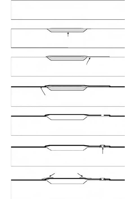
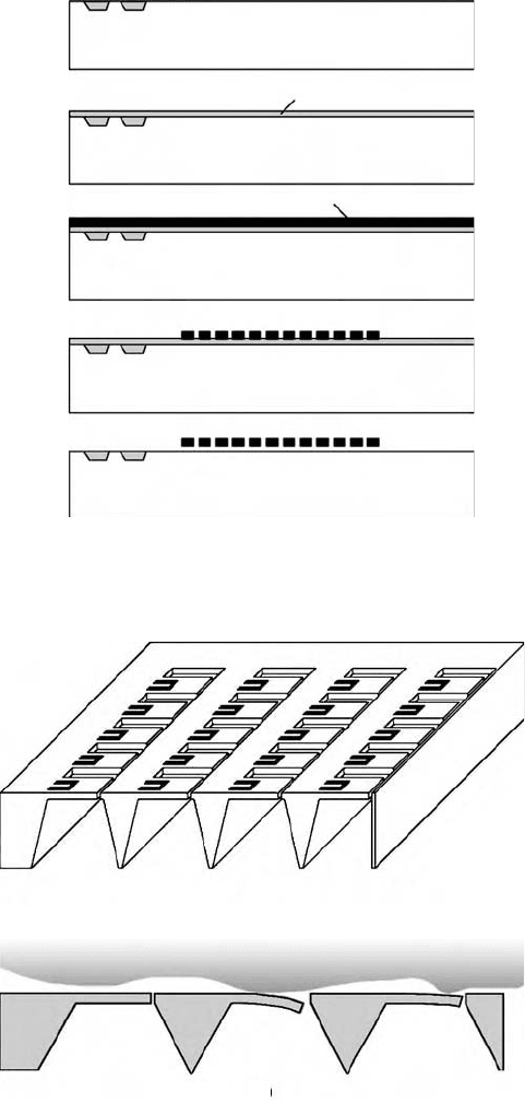
The fabrication process for a surface micromachined pressure sensor is shown in Figure 20.117. It starts
with a silicon substrate (a) with the front side polished. A local thermal oxidation process is performed
first to form a silicon oxide well with a typical thickenss of 1.3
µ
m. The thermal oxide is part of the sacrificial
layer that will be removed at a later stage. Using a process called low-pressure chemical vapor deposition
(LPCVD), a thin layer of oxide is again deposited over the wafer surface. This oxide layer is patterned
using the photolithography method (c). The entire wafer is coated with a silicon nitride thin film deposited
by LPCVD technique as well (d). The silicon nitride film is patterned and etched to produce an access
hole on top of the underlying oxide layer (e). Through this access hole, hydrofluoric acid removes the
oxide materials inside the cavity. The etch rate of the acid on silicon nitride is negligible (f). After the
cavity is emptied and dried, another layer of LPCVD silicon nitride is deposited to seal the opening in
the original silicon nitride layer (g). Following this step, polycrystalline silicon with suitable doping
concentration is deposited on top of the wafer and patterned to form the piezoresistors (h).
It should be noted that piezoresistive sensing, though dominant in the methods reviewed, is not the
only sensing mechanism available. Capacitive sensing and piezoelectric sensing are also feasible and have
been demonstrated in the past. However, discussions of these methods are beyond the scope of this text.
FIGURE 20.117 Schematic diagram of major steps for making a surface micromachined pressure sensor with silicon
nitride diaphragm.
(a)
(b)
(c)
(d)
(e)
(f)
(g)
(h)
Local thermal oxide
Deposited oxide film
Deposited silicon nitride film
Piezoresistors
Seal cavity
Starting silicon wafer
9258_C020_Sect_7-9.fm Page 144 Tuesday, October 9, 2007 9:09 PM
Sensors 20-145
Pressure Sensors Made of Non-Silicon Materials
For certain applications such as monitoring of internal combustion engine, pressure sensors are required
to sustain high temperature of operation. In such cases, silicon is not the optimal material because high
temperature causes doped silicon junctions to fail.
Work has also been done to implement polymer materials for pressure sensors. Though such devices
are relatively few, they represent an important development trend for future sensors.
20.9.2.3 Accelerometers
Bulk Micromachined Accelerometers
Acceleration sensors (or so-called inertial measurement units, IMU) are important for monitoring
acceleration and vibration experienced by a subject, such as an automobile, a machine, or a building.
Low-cost accelerometers used in automobile airbag deployment systems can reduce the costs and enhance
driver safety. Micromachined sensors can be made small and sufficiently low-cost to be used in smart
projectiles, for example, concrete penetrating bombs. Small, multi-axial accelerometers can also be applied
in writing instruments (smart pens) for handwriting recognition.
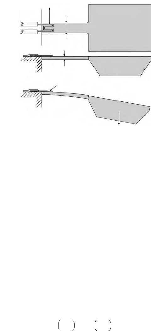
A representative bulk micromachined accelerometer is illustrated in Figure 20.118. A SEM micrograph
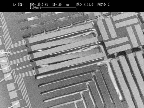
of a prototype sensor is shown in Figure 20.119. A silicon proof mass is attached to the end of a cantilever
beam. At the base of the cantilever beam lies a piezoresistive element. Supposing the mass of the proof
mass is m, and the magnitude of the acceleration is a, one can estimate the sensor output following a
few simple analysis steps. First, a concentrated force with a magnitude of F = ma is applied in the center
of the proof mass according to Newton’s first law. Secondly, the force translates into a torque loading at
the base of the cantilever with the magnitude being
The magnitude of the strain experienced at the surface of the cantilever beam, where the piezoresistors
are located, is
FIGURE 20.118 Schematic diagram of a bulk micromachined accelerometer.
(a) Top
view
(b) Side view
(zero acceleration)
(c) Side view
(finite acceleration)
Tensile stress
Proof mass (m)
F = ma
t
Piezoresistor
Metal
leads
MFl
L
2
---
+ ma l
L
2
---
+==
ε
Mt
2EI
--------
=
9258_C020_Sect_7-9.fm Page 145 Tuesday, October 9, 2007 9:09 PM
20-146 Mechatronic Systems, Sensors, and Actuators
Here, the term t is the thickness of the beam, E is the modulus of elasticity of the cantilever beam material,
and I is the momentum of inertia associated with the beam cross section. Supposing the cross section
of the cantilever beam is a rectangle with a width w and a thickness t, the moment of inertia is
Note that the moment of inertia is strongly related to the thickness of the beam. If the thickness of beam
is reduced to half, the magnitude of I is reduced by eight times, and the sensitivity of the sensor increases
by eight fold.
Surface Micromachined Accelerometers
Surface micromachined accelerometers offer the potential advantage of ready integration with signal
processing circuits. As a result, various types of surface micromachined versions have been made in the
past decade. A successful commercial product has been made by analog devices for sensing automobile
acceleration to deploy airbags in the events of collision. The structure, operational principle, and fabri-
cation process for such a sensor is briefly discussed in this section.
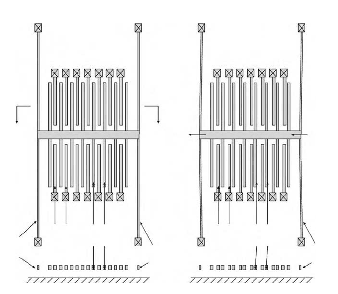
The sensor consists of two sets of interdigited comb-finger-shaped electrodes as shown in Figure 20.120.
One set of fingers is stationary and fixed to the substrate. Another set if suspended by cantilever springs
to the substrate. Capacitors are formed between each pair of comb-like fingers. When an external
acceleration is applied along the horizontal axis, an inertia force is applied to the moving set of fingers
and causes the moving fingers to displace. The amount of displacement is related to the magnitude of
the acceleration and the force constant of the supporting springs. The relative motion of the two sets of
fingers result in changes of the overall capacitance value between the two sets of fingers. The minute
capacitance change is sensed and processed by a signal-processing circuit consisting of an Σ − ∆ A/D
conversion stage [10].
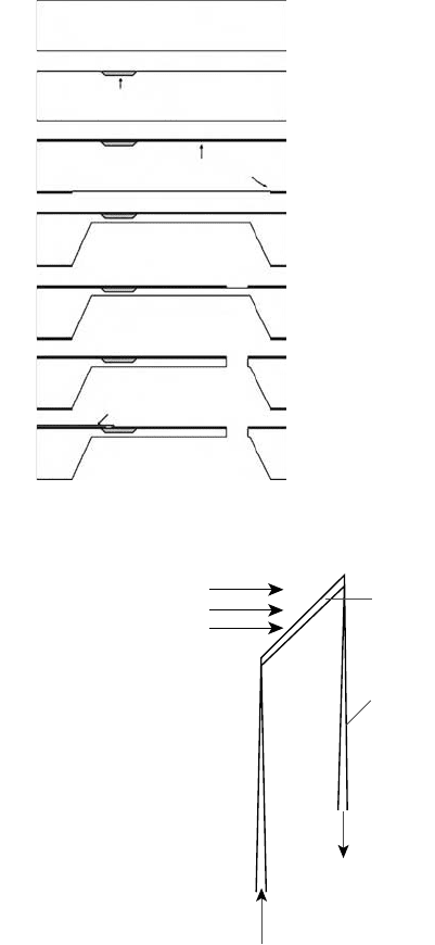
The fabrication process for such a sensor according to the A
–
A cross-section is illustrated in Figure 20.121.
First, transistors for signal processing circuits are first made on a silicon substrate (a). A sacrificial silicon
dioxide layer is deposited onto the wafer surface (b), followed by the deposition of a polycrystalline silicon
FIGURE 20.119 A SEM micrograph of a prototype bulk micromachined pressure sensor (Junjun Li).
I
wt
3
12
--------
=
9258_C020_Sect_7-9.fm Page 146 Tuesday, October 9, 2007 9:09 PM
Sensors 20-147
layer (c). The polycrystalline silicon is patterned and etched to form the comb fingers (e). Subsequently, the
oxide layer is removed by using a web etchant (hydrofluoric acid) that etches polycrystalline with negligible
rates. In areas where the polysilicon is anchored to the substrate, a via hole is patterned and etched in the
sacrificial layer before step (c).
20.9.2.4 Tactile Sensors
Tactile sensors are most widely used for robotics applications to provide tactile sensations for object
handling. The sensor density on a human fingertip is on the order of 100/cm
2
. Such a high sensor density
can be achieved using microfabrication technology.
An arrayed tactile sensor is illustrated in Figure 20.122. A two-dimensional array of individual sensor
elements provides two-dimensional mapping of contact force and shear force. The schematic cross-
sectional diagram of an array in contact with an arbitrary object is shown in Figure 20.122b. As an
object contacts a sensor beam, the amount of displacement corresponds to the contact force as well as
the surface topology.
The fabrication process of the tactile sensor is discussed in the following and illustrated in
Figure 20.123. Starting with a silicon wafer (a), a local ion implantation is first conducted to produce
piezoresistors (b). A thermal oxide film is grown to provide passivation to the entire wafer. The oxide
layer on the bottom of the wafer is patterned and etched to expose silicon substrates (c). An anisotropic
silicon etch is performed to remove silicon from the backside of the wafer (d). The oxide film on the
front of the wafer is then patterned and etched using plasma anisotropic etch to create free-standing
cantilever beams (e and f). Metal thin film is then deposited and patterned to provide lead wires (g).
FIGURE 20.120 Schematic diagram illustrating the operation principle of a surface micromachined accelerometer.
Side
view
Movable
fingers
Movable
fingers
Fixed
fingers
Equilibrium
(without acceleration)
Under acceleration
To p
view
AA’
ax
Fixed
fingers
Spring
support
Spring
support
Spring
support
SubstrateSubstrate
9258_C020_Sect_7-9.fm Page 147 Tuesday, October 9, 2007 9:09 PM
20-148 Mechatronic Systems, Sensors, and Actuators
20.9.2.5 Flow Sensors
Sensors for monitoring the flow rate of fluid (air or liquid) and for measuring the drag force exerted on
an object moving in a fluid have important applications in robotics applications. Existing flow sensors
are based on a number of principles, notably thermal and momentum transfer principles.
FIGURE 20.121 Schematic diagram of the fabrication process for a surface micromachined accelerometer illustrated
in the previous figure.
FIGURE 20.122 Schematic diagram of an array tactile sensor: (a) perspective view, (b) cross-sectional view.
(a)
(b)
(c)
(d)
(e)
Transistors
Transistors
Sacricicial oxide
Polysilicon
Transistors
Transistors
Transistors
(a)
(b)
9258_C020_Sect_7-9.fm Page 148 Tuesday, October 9, 2007 9:09 PM
Sensors 20-149
Flow Sensors Based on Heat Transfer Principles
For sensors based on thermal transfer principles, a heated element is used with temperature slightly
above the temperature of the ambient fluid (Figure 20.124). The heat is generally created by passing
current through a resistive element. An ideal element to serve as the heating element is doped
polysilicon resistor. The resistivity is generally lower than what can be achieved using metal resistors
of the same dimension, hence the resistance value is greater and the heating element can be made
smaller.
The movement of the fluid creates velocity-dependant forced convection of heat, thereby reducing the
temperature of the heated element accordingly. The temperature of the element is therefore used to
provide information about the flow rate and direction. Such sensors are commonly referred to as hot-
wire anemometers. Micromachined hot-wire anemometers have been demonstrated by several groups
[11,12].
FIGURE 20.123 Schematic diagram of the microfabrication process for realizing a tactile sensor.
FIGURE 20.124 Perspective diagram of a thermal-
transfer based flow sensor (anemometer).
(a)
(b)
(c)
(d)
(e)
(f)
(g)
Doped strain gauge
Thermally-grown oxide
Lead wire
Starting silicon substrate
Support
v
i
i
Heating
element/
sensor
9258_C020_Sect_7-9.fm Page 149 Tuesday, October 9, 2007 9:09 PM
20-150 Mechatronic Systems, Sensors, and Actuators
Flow Sensors Based on Momentum Transfer Principles
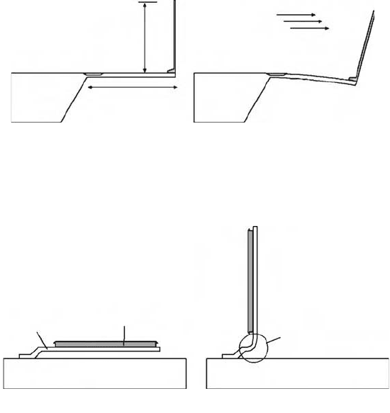
For sensors based on momentum transfer principles, a mechanical member is bent by the momentum
imparted by a moving fluid (Figure 20.125). The amount of the bending is used to decipher the strength
of the fluid flow. The schematic diagram of an exemplary flow sensor is shown in the figure below. It
consists of a vertical shaft attached to the end of a cantilever beam (a). When an external flow is
exerted, it will apply a distributed force onto the vertical shaft, hence causing the cantilever to bend.
The extent of the bending, as sensed by the embedded piezoresistor, is proportional to the average
flow rate.
The fabrication process is similar to the tactile sensor except for the attachment of the integrated
vertical shaft. A number of techniques for assembling three-dimensional microstructures using efficient
integrated processes have been developed in the past. For example, three-dimensional structures can be
realized using hinged microstructures and using solder joints or polymer joints. Recently, a process called
the plastic deformation magnetic assembly (PDMA) has been developed. In the following paragraph the
PDMA process is briefly discussed.
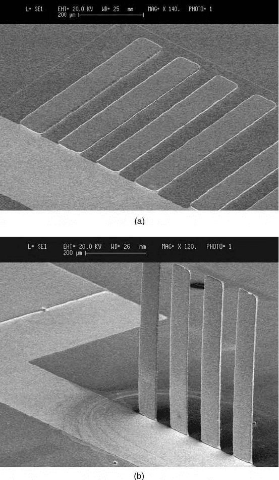
The PDMA technique is discussed using a simple surface micromachined cantilever as an example.
As shown in the diagram below (Figures 20.126 and 20.127), a single-clamped cantilever made of a
ductile metal (e.g., gold or aluminum) is suspended from the substrate. A piece of Permalloy, a
ferromagnetic alloy made by electrodeposition, is attached to the cantilever. When a magnetic field
is applied from underneath the wafer, the magnetic piece will be magnetized and will experience a
magnetic torque M. The torque lifts the cantilever beam away from the substrate. If the amount of
bending is significant, the ductile metal will be displaced permanently due to plastic deformation at
the hinge region.
FIGURE 20.125 Schematic diagram illustrating the operation principle of a momentum-transfer based flow sensor.
FIGURE 20.126 Schematic diagram of the plastic deformation magnetic assembly process.
(b) With flow(a) Without flow
Silicon
substrate
L
I
v
Substrate Substrate
Electroplated permalloy
Metal cantilever
Plastic
deformation
region
(a) (b)
9258_C020_Sect_7-9.fm Page 150 Tuesday, October 9, 2007 9:09 PM
Sensors 20-151
20.9.3 Future Development Trends
Miniaturization and integration of circuits has resulted in revolution in the society so far. It drastically
reduces the costs and increased the performance of circuits. Without the integrated circuits technology,
the information age would not have dawned on the human society.
It is conjectured that integrated microsensors are likely to produce as broad and deep an impact on
the society as the integrated circuits. Sensors can be used for robotics sensing, smart buildings, smart
FIGURE 20.127 SEM micrographs of cantilever beams (a) while in plane, and (b) after PDMA assembly.
9258_C020_Sect_7-9.fm Page 151 Tuesday, October 9, 2007 9:09 PM
20-152 Mechatronic Systems, Sensors, and Actuators
toys, automotive safety and control, and industrial control. However, in order to realize the advantages
of integrated sensors, a number of technical barriers must be overcome. Two important barriers are (1)
high R&D costs of integrated sensors and (2) reliable and robust packaging of sensors.
The development of microintegrated sensors involves high development costs and long time-to-
market. The surface micromachined accelerometer developed by analog devices costs tens of millions of
dollars and took more than 5 years to produce. Why do integrated sensors cost so much to build? Sensors
are developed using a group-up approach. The development cycle of a sensor begins at the level of physical
principles. The cost of sensor development includes expertise for material selection, design generation,
prototype process development, and characterization.
Such a development cost and speed is not tolerable in applications where only a small amount of
custom sensors is required. Standard sensing modules, low-cost, flexible foundry fabrication processes,
and advanced computer simulation and prototyping tools are required to advance the state-of-the-art
of microintegrated sensors.
Future sensors will involve more non-silicon materials. For example, polymer materials can be used
to reduce the costs while high-temperature materials maybe used for high-temperature sensing applica-
tions (e.g., monitoring of conditions in engines).
20.9.4 Conclusions
A brief historical overview of the development of microfabrication technology and microintegrated
sensors is presented. Common sensing principles, including capacitive, piezoresistive, and piezoelectric
sensing, are discussed. Four important case studies of sensors are undertaken. For each type of sensor
applications—pressure sensors, acceleration sensors, tactile sensors, and flow sensors—the sensor archi-
tectures and fabrication processes are reviewed. Interested readers may find more in-depth information
in the references provided in this section.
References
1. Nathanson, H.C., Newell, W.E., Wickstrom, R.A., and Davis J.R. Jr., “The resonant gate transistor,”
IEEE Transactions on Electron Devices, Vol. ED-14, No. 3, pp. 117–113, March 1967.
2. Petersen, K.E., “Silicon as a mechanical material,” Proceedings of the IEEE, Vol. 70, No. 5, pp. 420–457,
May 1982.
3. Angell, J.B., Terry, S.C., and Barth, P.W., “Silicon micromechanical devices,” Scientific American, Vo l.,
248, pp. 44–55, April 1983.
4. Siewell, G.L., Boucher, W.R., and McClelland, P.H., “The ThinkJet orifice plate: a part with many
functions,” Hewlett-Packard Journal, May 1985, pp. 33–37.
5. Allen, R.R., Meyer, J.D., and Knight, W.R., “Thermodynamics and hydrodynamics of thermal ink
jets,” Hewlett-Packard Journal, May 1985, pp. 21–27.
6. Williams, K.R., and Muller, R.S., “Etch rates for micromachining processing,” Journal of Microelec-
tromechanical Systems, Vol. 5, No. 4, pp. 256–268, December 1996.
7. Kovacs, G.T.A., Micromachined transducers sourcebook, McGraw-Hill, 1998.
8. Trimmer, W.S., Micromechanics and MEMS––Classis and seminal papers to 1990, IEEE Press, 1997.
9. WWW site http://mems.isi.edu.
10 Yun, W., Howe, R.T., and Gray, P.R., “Surface micromachined, digitally force-balanced accelerometer
with integrated CMOS detection circuitry,” Technical D igest, IEEE Solid-State Sensor and Actuator
Workshop, pp. 21–25, Hilton Head, SC, June 1992.
11. Jiang, F., Tai, Y.C., Ho, C.M., Karan, R., and Garstenauer, M., “Theoretical and experimental studies
of micromachined hot-wire anemometers,” Technical Digest, International Electron Devices Meeting
1994, San Francisco, CA, pp. 139–142, December 1994.
12. Ebefors, T., Kalvesten, E., and Stemme, G., “Three dimensional silicon triple-hot-wire anemometer
based on polyimide joints,” Proceedings of the 11th International Workshop on MEMS, pp. 93–98,
January 1998.
9258_C020_Sect_7-9.fm Page 152 Tuesday, October 9, 2007 9:09 PM

21-1
21
Actuators
21.1 Electromechanical Actuators ............................... 21-1
Introduction
•
Type of Electromechanical
Actuators—Operating Principles
•
Power Amplification
and Modulation—Switching Power Electronics
•
References
21.2 Electrical Machines .................................................. 21-33
DC Motor
•
Armature Electromotive Force (emf)
•
Armature Torque
•
Terminal Voltage
•
Methods of
Connection
•
Starting DC Motors
•
Speed Control of DC
Motors
•
Efficiency of DC Machines
•
AC
Machines
•
Motor Selection
•
References
21.3 Piezoelectric Actuators ............................................ 21-51
Piezoeffect Phenomenon
•
Constitutive Equations
•
Piezomaterials
•
Piezoactuating Elements
•
Application
Areas
•
Piezomotors (Ultrasonic Motors)
•
Piezoelectric
Devices with Several Degrees of Freedom
•
References
21.4 Hydraulic and Pneumatic Actuation Systems ........ 21-63
Introduction
•
Fluid Actuation Systems
•
Hydraulic
Actuation Systems
•
Modeling of a Hydraulic Servosystem
for Position Control
•
Pneumatic Actuation
Systems
•
Modeling a Pneumatic Servosystem
•
References
21.5 MEMS: Microtransducers Analysis,
Design, and Fabrication .......................................... 21-97
Introduction
•
Design and Fabrication
•
Analysis of
Translational Microtransducers
•
Single-Phase Reluctance
Micromotors: Microfabrication, Modeling, and
Analysis
•
Three-Phase Synchronous Reluctance
Micromotors: Modeling and Analysis
•
Microfabrication
Aspects
•
Magnetization Dynamics of Thin
Films
•
Microstructures and Microtransducers with
Permanent Magnets: Micromirror Actuator
•
Micromachined Polycrystalline Silicon Carbide
Micromotors
•
Axial Electromagnetic
Micromotors
•
Conclusions
•
References
21.1 Electromechanical Actuators
George T.-C. Chiu
21.1.1 Introduction
As summarized in the previous chapter, a mechatronics system can be partitioned into function blocks
illustrated in Figure 21.1. In this chapter, we will focus on the actuator portion of the system. Specifically,
we will present a general discussion of the types of electromechanical actuators and their interaction
George T.-C. Chiu
Purdue University
Charles J. Fraser
University of Abertay Dundee
Habil Ramutis Bansevicius
Rymantas Tadas Tolocka
Kaunas University of Technology
Massimo Sorli
Stefano Pastorelli
Politecnico di Torino
Sergey Edward Lyshevski
University of Rochester
9258_C021_Sect001.fm Page 1 Wednesday, October 10, 2007 7:09 PM