Chung Y.-W. Practical guide to surface science and spectroscopy
Подождите немного. Документ загружается.

107
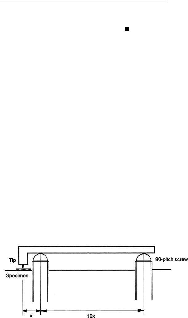
6.6 STM IMPLEMENTATION
to map the spatial distribution of gold and platinum atoms on the
surface of a gold–platinum binary alloy.
6.6 STM IMPLEMENTATION
6.6.1 Coarse Motion Control
In order to bring the tip to within tunneling range, one must move
the tip over macroscopic distances (hundreds of micrometers) with a
reasonable precision of several tens of nanometers. Several schemes
are possible. In the original work by Binnig and Rohrer, they used a
piezoelectric inchworm (more on piezoelectric materials later). Some
designs are based on purely mechanical means, all using fine-thread
screws. One example is shown in Fig. 6.2. Consider a conventional
80-pitch screw, that is, the screw advances by one inch (2.54 cm) after
80 turns. This translates into a motion advance of about 880 nm for
1⬚ of screw rotation. Using a cantilever beam with a velocity ratio of
10, one achieves a precision of 88 nm for 1⬚ of screw rotation.
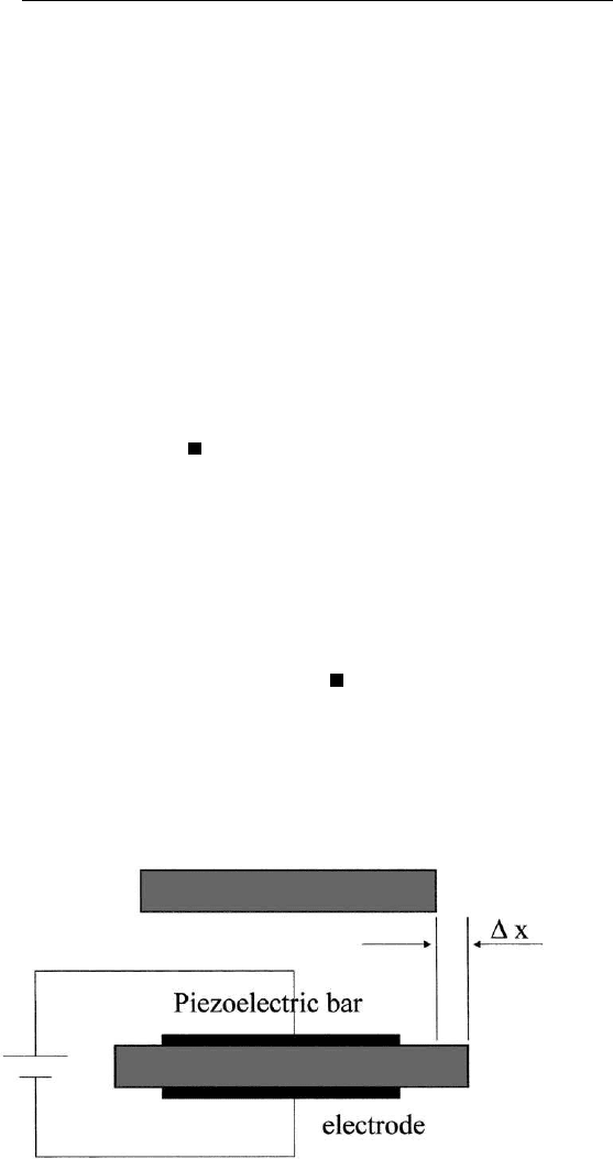
6.6.2 Fine Motion Control
During tunneling and feedback control, the precision required for tip
positioning relative to the specimen surface must be better than 0.1
nm. This is achieved by using piezoelectric positioners. Piezoelectric
materials expand or contract upon the application of an electric field
FIGURE 6.2 Example of coarse approach using a fine-thread screw and the reduced
velocity ratio of a cantilever beam.
108
CHAPTER6/SCANNING PROBE MICROSCOPY
(Fig. 6.3). In this configuration, the piezoelectric response coefficient
of interest is d
31
(m/V). Upon the application of an electric field E in
the direction shown, the length of the piezoelectric bar will increase
or decrease by d
31
EL, where L is the initial length of the bar. Although
many materials exhibit the piezoelectric effect, lead zirconium titanate
(PZT) is the material of choice in the STM community, with typical
d
31
values ⬇ 10
⫺10
m/V.
E
XAMPLE.
Consider a piezoelectric bar of length 2 cm and thick-
ness 1 mm. Calculate the extension upon the application of 150 V
across the thickness of the bar, assuming a d
31
value of 5 ⫻ 10
⫺10
m/V.
S
OLUTION.
The electric field E ⫽ 150 / 0.001 ⫽ 1.5 ⫻ 10
5
V/m.
Therefore, the length change ⫽ d
31
EL⫽ 5 ⫻ 10
⫺10
⫻ 1.5 ⫻ 10
5
⫻ 0.02 m ⫽ 1.5
m.
Most STMs are designed with a scanning range from 1 to 10 m, with
some commercial versions going up to 150 m. In the example cited
above, the response is 10 nm/V. Since voltages can be controlled and
monitored in the submillivolt level easily, subnanometer control can
be readily attained.
Q
UESTION FOR
D
ISCUSSION.
What are the criteria for choosing a
piezoelectric material for the STM?
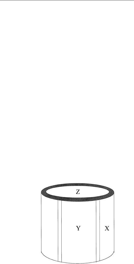
In the initial development of STMs, three-axis control was accom-
plished using three separate pieces of piezoelectric bars held together
in an orthogonal arrangement. To improve rigidity especially for long
scanners, most researchers opt for a design based on a piezoelectric
FIGURE 6.3 Illustration of the piezoelectric effect.
109
6.6 STM IMPLEMENTATION
tube scanner, shown in Fig. 6.4. The inside of the piezoelectric tube
is completely metal-coated, while the outside is metal-coated in four
separate quadrants. By applying appropriate voltages to one pair of
diametrically opposite quadrants, one causes the piezoelectric tube to
bend along that direction, thus achieving X or Y scanning motion.
Application of voltage to the inner surface causes the tube to expand
or contract (Z-axis motion). Three-axis motion can thus be attained
with a single tube. The lowest resonance frequency of tube scanners
can be made to exceed 10 kHz easily (cf. typically 1 kHz for orthogonal
tripods). This higher resonance frequency allows electronic feedback
and scanning at higher rates without setting the scanner into resonance
or crashing the tip onto the specimen surface. The major disadvantage
of the tube scanner is cross-talk among the three axes resulting in
nonorthogonal motion.
6.6.3 Tip Preparation
Two types of tip materials are widely used, viz., tungsten and platinum
alloys (e.g., Pt–Ir and Pt–Rh). Tungsten is strong and can be fabricated
into sharp tips easily. But it tends to oxidize rapidly in air. On the other
hand, Pt alloys are stable in air, but they may not survive occasional
tip crashes on surfaces.
Several methods can be used to create sharp tips of these materials.
These include electropolishing, cutting and grinding, momentary appli-
FIGURE 6.4 A piezoelectric tube scanner.
110
CHAPTER6/SCANNING PROBE MICROSCOPY
cation of a high bias voltage (a few volts), or simply waiting for a few
minutes after setting up in the tunneling configuration. In order to
image rough surfaces, tips with large aspect ratios should be used.
Q
UESTION FOR
D
ISCUSSION.
Why should tips with large aspect
ratios be used in imaging rough surfaces? Do we have the same require-
ments for smooth surfaces?
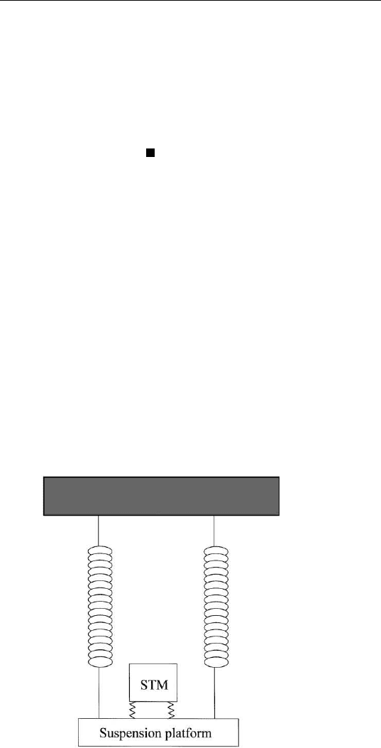
6.6.4 Vibration Isolation
The first tunneling microscope was supported using superconducting
levitation for vibration isolation. More recent designs used damped
springs, air tables, and stacked stainless steel plates separated by viton
dampers. The goal in all these designs is to keep the tip–surface spacing
immune to external vibrations. Assume that the STM sits on a platform
that is coupled to the outside world via a spring with resonance fre-
quency f and that the lowest resonance frequency of the STM is F,
which is much greater than f (Fig. 6.5). The external vibration has a
frequency f ⬘ and amplitude A. With such a system, the vibration ampli-
tude transmitted to the STM depends on the frequency f ⬘ of the vibra-
tion. There are four regimes to consider:
FIGURE 6.5 Vibration isolation for a scanning tunneling microscopy using springs.

111
6.6 STM IMPLEMENTATION
(a) f ⬘ ⬍ f. The platform spring does nothing to attenuate the exter-
nal vibration. The vibration amplitude entering into the microscope
causes a tip–surface spacing change a given by
a ⫽ A
冉
f⬘
F
冊
2
. (6.9)
(b) f ⬘ ⬇ f. The vibration amplitude entering into the microscope
is actually amplified, depending on the amount of damping in the
platform spring.
(c) f « f ⬘ « F. In this case, the vibration amplitude a entering into
the microscope is independent of f ⬘ and is given by
a ⫽ A
冉
f
F
冊
2
. (6.10)
(d) f ⬘ » F. Only the platform spring does the attenuation, and the
transmitted vibration amplitude a is given by
a ⫽ A
冉
f
f⬘
冊
2
. (6.11)
In examining these four cases, it becomes clear that one should support
the STM on a soft platform (small f ) and design a microscope with
high rigidity (large F). For example, for case (c) with f ⫽ 1 Hz, F ⫽
10 kHz, and A ⫽ 10 m, the transmitted vibration amplitude is equal
to 10
⫺4
nm for intermediate frequencies. Therefore, a rigid STM not
only allows fast image acquisition, but also more effective vibration
isolation.
6.6.5 Data Acquisition and Analysis
A typical setup is shown in Fig. 6.6. A voltage bias is applied between
the tip and the specimen. The tunneling current so obtained is then
compared between a preset value (typically 1–10 nA). The error signal
then drives a feedback circuit whose output is used to control a fast,
high-voltage operational amplifier that feeds voltage to the Z electrode
of the tube scanner. At the same time, raster-scanning is accomplished
by using two digital-to-analog converters to control the output of two
high-voltage operational amplifiers feeding voltages to the X and Y
electrodes of the tube scanner. At each step, the Z voltage required to
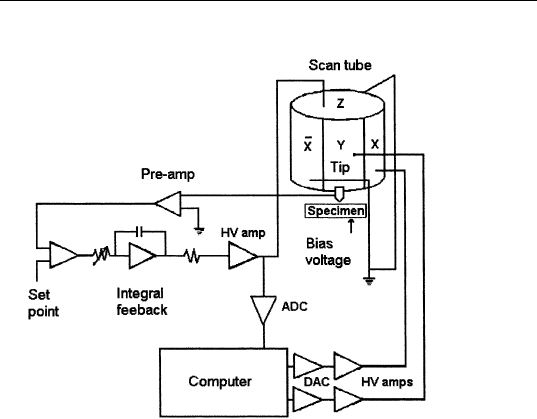
112
CHAPTER6/SCANNING PROBE MICROSCOPY
FIGURE 6.6 A typical data acquisition setup for STM.
maintain a constant tunneling current is read by the computer via
an analog-to-digital converter. This Z voltage, as discussed earlier,
corresponds to the surface height at that XY location. This information
can then be displayed in real time as gray-level images on a video
monitor. Most tube-based scanners allow image acquisition at the rate
of several thousand pixels per second.
In such a setup, feedback control is done by analog circuitry.
Software feedback is now feasible with the availability of fast digital
signal processors. Normally, topographical data are stored as two-
dimensional integer arrays. As a result, each image can be processed
in a variety of ways, for example, to suppress noise, to enhance parts
of the image, or to obtain certain surface roughness parameters. Com-
mercial software packages are available for these types of image
processing and analysis on personal computers and workstations. Hard-
copy outputs can be obtained as line plots or gray-level images.
6.7 APPLICATIONS OF STM
6.7.1 High-Resolution Imaging of Surfaces
The most direct application of the STM is to obtain topography of
surfaces at high resolution, either for atomic imaging or for general
surface roughness determination. Many studies on imaging of biological
113
6.7 APPLICATIONS OF STM
molecules have been reported. The advantage with the STM is its
ability to image with high resolution under normal air or aqueous
environments so that no additional specimen processing is required.
Q
UESTION FOR
D
ISCUSSION
One often hears comments that the
spatial resolution of a given microscopy technique is limited by the
wavelength of the probe. For example, optical microscopy has a resolu-
tion limit on the order of a micron. However, with the STM using an
electon energy of 10 meV (corresponding wavelength about 10 nm),
one can resolve carbon atoms on graphite easily. Discuss this apparent
paradox.
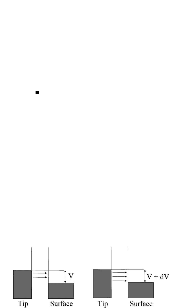
6.7.2 Spectroscopy
At a fixed tip–surface separation, when one changes the bias voltage
from V to V⫹dV as shown in Fig. 6.7, the tunneling current increases
because of the availability of more electrons from the tip and more
empty states from the surface for tunneling. If the density of states of
the tip is known, one can recover the density of empty states for the
surface from such current–voltage measurements. By reversing the
applied bias, the density of occupied states for the surface can be
obtained as well.
6.7.3 Lithography
Because of the nature of tunneling, the tunneling current is self-focused
into a diameter of a fraction of a nanometer. For a tunneling current
of 10 nA, the current density is ⬃1 ⫻ 10
6
A/cm
2
. At sufficiently
high bias voltages, it is possible to induce chemical reactions over the
FIGURE 6.7 Illustration of current–voltage spectroscopy.

114
CHAPTER6/SCANNING PROBE MICROSCOPY
nanometer scale, analogous to photolithography. It has been demon-
strated that the STM can produce patterns with line widths on the order
of 10 nm.
6.7.4 Current Fluctuations
Electron traps may exist on surfaces (e.g., electronic states located in
the bandgap of semiconductors or poorly conducting species). When
a tunneling electron impinges on the surface and is captured by these
charge traps, the local potential becomes more negative and suppresses
further tunneling. This results in a drop of the tunneling current. Some
time later, the electron is released from the trap, resulting in resumption
of normal tunneling. The net result is that the tunneling current fluctu-
ates with time at these trap sites. Therefore, this provides a method for
imaging these electron traps. Further, by measuring how the rate of
tunneling current fluctuation as a function of tunneling bias, it is possible
to determine the energy location of these electron traps. For further
information, see the articles by M. E. Welland and R. H. Koch, Appl.
Phys. Lett. 48, 724 (1986), and R. H. Koch and R. J. Hamers, Surf.
Sci. 181, 333 (1987).
6.8 LIMITATIONS OF STM AND SOLUTIONS
There are two major limitations of the STM. First, the specimen surface
must be reasonably conducting. Under typical operation conditions,
the resistance of the gap separating the tip and the specimen is on the
order of 10 megaohms (e.g., tunneling at 1 nA under a bias of 10 mV).
‘‘Reasonably conducting’’ means that the resistance of the electrical
path from the specimen to the return circuit should be small compared
with 10 megaohms. This rules out many ceramic and polymer materials
from consideration. One solution is to put a conduction coating (e.g.,
gold) on such surfaces, assuming that the coating faithfully reproduces
the surface topography of the substrate. Another solution is to use AC
tunneling, i.e., the bias is allowed to change sign rapidly. The basic
idea is that in the forward cycle, electrons are injected from the tip
onto the surface. The behavior of the tunneling current with respect to
tip–surface spacing is as predicted by Eq. (6.3) in this portion of the
cycle. Therefore, feedback control can be ‘‘locked’’ to the tunneling
current in the forward cycle. In the next half cycle, the polarity is

115
6.10 ATOMIC FORCE MICROSCOPY
reversed, thereby clearing electrons from the surface of the insulating
specimen. In this way, insulating surfaces can be imaged by the STM.
The major difficulty is that high-frequency AC bias may be required
for highly insulating surfaces. Stray capacitance between the tip and
the sample may result in a large displacement current that can over-
whelm the tunneling current.
Second, the STM suffers from limited scanning range. Using rea-
sonable geometry (e.g., scan head on the order of a few centimeters.
long, scan tube thickness of 1 to 2 mm) and applied voltage (e.g., not
exceeding 300–400 V), one finds that the maximum scan range is on
the order of 100 m. In general, longer scanners have lower resonance
frequencies so that scanning rates must be reduced to obtain images
over large areas.
6.9 SCANNING CAPACITANCE MICROSCOPY
One variant of the STM is scanning capacitance microscopy (SCaM).
In SCaM, one uses the capacitance between the tip and the specimen
surface as a sensor of the tip–surface spacing. In spite of the very small
capacitance involved in these measurements (about 0.1–1 ⫻ 10
⫺18
F),
spatial resolution of about 25 nm has been demonstrated. In addition,
by exploiting the fact that the capacitance of a semiconductor surface
depends on the carrier concentration, one can use this technique to
image dopant distribution on semiconductor surfaces at high spatial
resolution. One advantage of SCaM is that it can be applied to insulator
surfaces.
6.10 ATOMIC FORCE MICROSCOPY
In atomic force microscopy (AFM), one senses the force of interaction
between the tip and the specimen surface. The tip is normally part of
a small wire or microfabricated cantilever. The tip–surface interaction
results in deflection of the cantilever. In most designs, the cantilever
deflection is sensed either by detecting the reflection of a laser beam
from the back of the cantilever or by optical interferometry. In one
design, the deflection is measured by a (piezoelectric) sensing element
deposited on the cantilever. Under appropriate operation conditions,
atomic resolution can be achieved. One important strength of the AFM

116
CHAPTER6/SCANNING PROBE MICROSCOPY
is its ability to obtain images from insulator surfaces. Also, magnetic
domains can be imaged using a magnetized tip. One can readily adapt
an atomic force microscope either as a microtribometer (studying fric-
tion) or as a nanoindentor (studying surface mechanical properties).
6.10.1 Equations of Interest
(a) Spring constant of a cantilever (C ):
C ⫽ 0.25 ⫻ b(d/L)
3
E
where b is the width, d thickness, E Young’s modulus, and L the
length.
(b) Resonance frequency of a cantilever ( f ):
f ⫽ 0.162 (d/L
2
)(E/
)
1/2
,
being the material density.
(c) Thermal noise amplitude (a
th
):
a
th
⫽ (kT/C)
1/2
.
E
XAMPLE.
For a cantilever of width 25
m, thickness 25
m, and
length 500
m, made of material with a modulus of 70 GPa and
density 5 g/cm
3
, calculate the spring constant, resonance frequency,
and thermal noise amplitude at room temperature.
S
OLUTION.
b ⫽ 25
m ⫽ d; L ⫽ 500
m
C ⫽ 0.25 ⫻ (25 ⫻ 10
⫺6
) ⫻ (25/500)
3
⫻ (70 ⫻ 10
9
)
⫽ 54.7 N/m
f ⫽ 0.162 ⫻ (25 ⫻ 10
⫺6
/25 ⫻ 10
⫺8
) ⫻ (70 ⫻ 10
9
/5000)
1/2
⫽ 60.6 kHz
a
th
⫽ (1.38 ⫻ 10
⫺23
⫻ 300/55)
1/2
⫽ 0.009 nm.
PROBLEMS
1. Consider the situation when the STM tip is connected to the
specimen surface through a rigid coupling with resonance fre-
quency
o
. Vibration of amplitude A ⫽ A
o
exp(it) is applied to