Hawkes P.W., Spence J.C.H. (Eds.) Science of Microscopy. V.1 and 2
Подождите немного. Документ загружается.

65
2
Scanning Transmission
Electron Microscopy
Peter D. Nellist
1. Introduction
The scanning transmission electron microscope (STEM) is a very pow-
erful and highly versatile instrument capable of atomic resolution
imaging and nanoscale analysis. The purpose of this chapter is to
describe what STEM is, to highlight some of the types of experiments
that can be performed using a STEM, to explain the principles behind
the common modes of operation, to illustrate the features of typical
STEM instrumentation, and to discuss some of the limiting factors in
its performance.
1.1 The Principle of Operation of a STEM
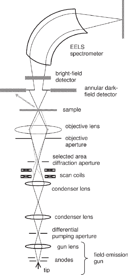
Figure 2–1 shows a schematic of the essential elements of a STEM. Most
dedicated STEM instruments have their electron gun at the bottom of
the column with the electrons traveling upward, which is how Figure
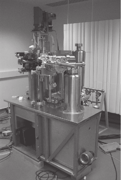
2–1 has been drawn. Figure 2–2 shows a photograph of a dedicated
STEM instrument.
More commonly available at the time of writing are combined con-
ventional transmission electron microscope (CTEM)/STEM instru-
ments. These can be operated in both the CTEM mode, where the
imaging and magnifi cation optics are placed after the sample to provide
a highly magnifi ed image of the exit wave from the sample, or the
STEM mode as described in Section 8. Combined CTEM/STEM instru-
ments are derived from conventional transmission electron micro-
scopy (TEM) columns and have their gun at the top of the column. The
pertinent optical elements are identical, and for a TEM/STEM Figure
2–1 should be regarded as being inverted.
In many ways, the STEM is similar to the more widely known scan-
ning electron microscope (SEM). An electron gun generates a beam of
electrons that is focused by a series of lenses to form an image of the
electron source at a specimen. The electron spot, or probe, can be
scanned over the sample in a raster pattern by exciting scanning defl ec-
tion coils, and scattered electrons are detected and their intensity
66
Figure 2–1. A schematic of the essential elements of a dedicated STEM instru-
ment showing the most common detectors.
plotted as a function of probe position to form an image. In contrast to
an SEM, where a bulk sample is typically used, the STEM requires a
thinned, electron transparent specimen. The most commonly used
STEM detectors are therefore placed after the sample, and detect trans-
mitted electrons.
Since a thin sample is used (typically less than 50 nm thick), the
probe spreading within the sample is relatively small, and the spatial
resolution of the STEM is predominantly controlled by the size of the
probe. The crucial image forming optics are therefore those before the
Peter D. Nellist
Chapter 2 Scanning Transmission Electron Microscopy 67
sample that are forming the probe. Indeed the short-focal-length lens
that fi nally focuses the beam to form the probe is referred to as the
objective lens. Other condenser lenses are usually placed before the
objective to control the degree to which the electron source is demagni-
fi ed to form the probe. The electron lenses used are comparable to
those in a conventional TEM, as are the electron accelerating voltages
used (typically 100–300 kV). Probe sizes below the interatomic spacings
in many materials are often possible, which is the great strength of
STEM. Atomic resolution images can be readily formed, and the probe
can then be stopped over a region of interest for spectroscopic analysis
at or near atomic resolution.
To form a small, intense probe we clearly need a correspondingly
small, intense electron source. Indeed, the development of the cold fi eld
emission gun by Albert Crewe and co-workers nearly 40 years ago
(Crewe et al., 1968a) was a necessary step in their subsequent construc-
tion of a complete STEM instrument (Crewe et al., 1968b). The quantity
of interest for an electron gun is actually the source brightness, which
will be discussed in Section 9. Field-emission guns are almost always
Figure 2–2. A photograph of a d edicated STEM instrument (VG Microscopes
HB501). The gun is below the table level, with most of the electron optics above
the table. At the top of the column can be seen a magnetic prism spectrometer
for electron energy-loss spectroscopy.
68
used for STEM, either a cold fi eld emission gun (CFEG) or a Schottky
thermally assisted fi eld emission gun. In the case of a CFEG, the source
size is typically around 5 nm, so the probe-forming optics must be
capable of demagnifying its image of the order of 100 times if an atomic
sized probe is to be achieved. In a Schottky gun the demagnifi cation
must be even greater.
The size of the image of the source is not the only probe size defi ning
factor. Electron lenses suffer from inherent aberrations, in particular
spherical and chromatic aberrations. The aberrations of the objective
lens generally have greatest effect, and limit the width of the beam
that may pass through the objective lens and still contribute to a small
probe. Aberrated beams will not be focused at the correct probe posi-
tion, and will lead to large diffuse illumination thereby destroying
the spatial resolution. To prevent the higher angle aberrated beams
from illuminating the sample, an objective aperture is used, and is
typically a few tens of microns in diameter. The existence of an
objective aperture in the column has two major implications: (1) As
with any apertured optical system, there will be a diffraction limit
to the smallest probe that can be formed, and this diffraction limit
may well be larger than the source image. (2) The current in the
probe will be limited by the amount of current that can pass through
the aperture, and much current will be lost as it is blocked by the
aperture.
Because the STEM resembles the more commonly found SEM in
many ways, several of the detectors that can be used are common to
both instruments, such as the secondary electron (SE) detector and the
energy-dispersive X-ray (EDX) spectrometer. The highest spatial reso-
lution in STEM is obtained by using the transmitted electrons, however.
Typical imaging detectors used are the bright-fi eld (BF) detector and
the annular dark-fi eld (ADF) detector. Both these detectors sum the
electron intensity over some region of the far fi eld beyond the sample,
and the result is displayed as a function of probe position to generate
an image. The BF detector usually collects over a disc of scattering
angles centered on the optic axis of the microscope, whereas the ADF
detector collects over an annulus at higher angle where only scattered
electrons are detected. The ADF imaging mode is important and unique
to STEM in that it provides incoherent images of materials and has a
strong sensitivity to atomic number allowing different elements to
show up with different intensities in the image.
Two further detectors are often used with the STEM probe stationary
over a particular spot: (1) A Ronchigram camera can detect the inten-
sity as a function of position in the far fi eld, and shows a mixture of
real-space and reciprocal-space information. It is mainly used for
microscope diagnostics and alignment rather than for investigation of
the sample. (2) A spectrometer can be used to disperse the transmitted
electrons as a function of energy to form an electron energy-loss (EEL)
spectrum. The EEL spectrum carries information about the composi-
tion of the material being illuminated by the probe, and even can show
changes in local electron structure through, for example, bonding
changes.
Peter D. Nellist
Chapter 2 Scanning Transmission Electron Microscopy 69
1.2 Outline of Chapter
The crucial aspect of STEM is the ability to focus a small probe at a
thin sample, so we start by describing the form of the STEM probe and
how it is computed. To understand how images are formed by the BF
and ADF detectors, we need to know the electron intensity distribution
in the far fi eld after the probe has been scattered by the sample, which
is the intensity that would be observed by a Ronchigram camera. This
allows us to go on and consider BF and ADF imaging.
Moving on to the analytical detectors, there is a section on the EEL
spectrum that emphasizes some aspects of the spatial localization of
the EEL spectrum signal. Other detectors, such as EDX and SE, that are
also found on SEM instruments are briefl y discussed.
Having described STEM imaging and analysis we return to some
instrumental aspects of STEM. We discuss typical column design, and
then go on to analyze the requirements for the electron gun in STEM.
Consideration of the effect of the fi nite gun brightness brings us to a
discussion of the resolution limiting factors in STEM where we also
consider spherical and chromatic aberrations. We fi nish that section
with a discussion of spherical aberration correction in STEM, which is
arguably having the greatest contribution in the fi eld of STEM and is
producing a revolution in performance.
There have been several review articles previously published on
STEM (for example, Cowley, 1976; Crewe, 1980; Brown, 1981). More
recently, instrumental improvements have increased the emphasis on
atomic resolution imaging and analysis. In this chapter we tend to focus
on the principles and interpretation of STEM data when it is operating
close to the limit of its spatial resolution.
2. The STEM Probe
The crucial aspect of STEM performance is the ability to focus a sub-
nanometer-sized probe at the sample, so we start by examining the
form of that probe. We will initially assume that the electron source is
infi nitesimal, and that the beam is perfectly monochromatic. The
effects of these assumptions not holding are explored in more detail
in Section 10.
The probe is formed by a strong imaging lens, known as the objective
lens, that focuses the electron beam down to form the crossover that
is the probe. Typical electron wavelengths in the STEM range from
3.7 pm (for 100-keV electrons) to 1.9 pm (for 300-keV electrons), so we
might expect the probe size to be close to these values. Unfortunately,
all circularly symmetric electron lenses suffer from inherent spherical
aberration, as fi rst shown by Scherzer (1936), and for most TEMs this
has typically limited the resolution to about 100 times worse that the
wavelength limit.
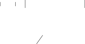
The effect of spherical aberration from a geometric optics standpoint
is shown in Figure 2–3. Spherical aberration causes an overfocusing of
the higher angle rays of the convergent beam so that they are brought
to a premature focus. The Gaussian focus plane is defi ned as the plane
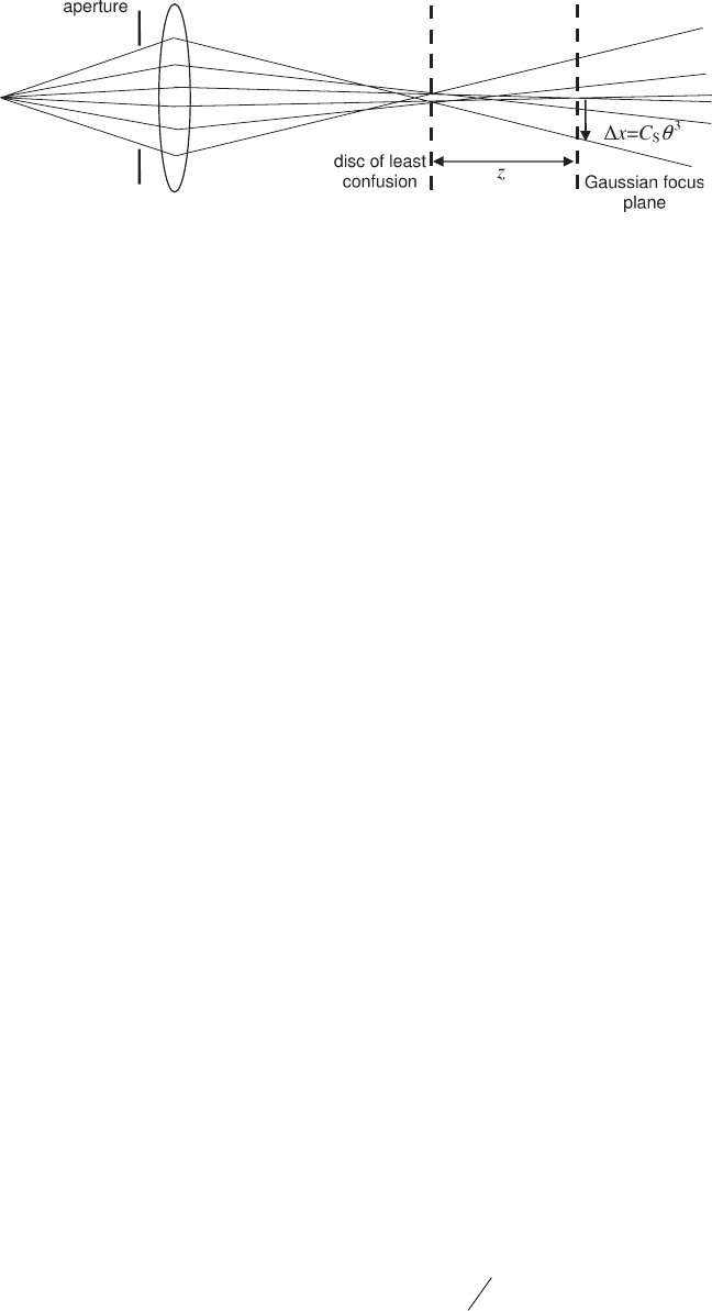
70
at which the beams would have been focused had they been unaber-
rated. At the Gaussian plane, spherical aberration causes the beams to
miss their correct point by a distance proportional to the cube of the
angle of ray. Spherical aberration is therefore described as being a third-
order aberration, and the constant of proportionality is given the
symbol, C
S
, such that
∆x = C
S
θ
3
(2.1)
If the convergence angle of the electron beam is limited, then it can be
seen in Figure 2–3 that the minimum beam waist, or disc of least confu-
sion, is located closer to the lens than the Gaussian plane, and that the
best resolution in a STEM is therefore achieved by weakening or under-
focusing the lens relative to its nominal setting. Underfocusing the lens
compensates to some degree for the overfocusing effects of spherical
aberration.
The above analysis is based upon geometric optics, and ignores the
wave nature of the electron. A more quantitative approach is through
wave optics. Because the lens aberrations affect the rays converging to
form the probe as a function of angle, they can be incorporated as a
phase shift in the front-focal plane (FFP) of the objective lens. The FFP
and the specimen plane are related by a Fourier transform, as per the
Abbe theory of imaging (Born and Wolf, 1980). A point in the front-
focal plane corresponds to one partial-plane wave within the ensemble
of plane waves converging to form the probe. The defl ection of the ray
by a certain distance at the sample corresponds to a phase gradient in
the FFP aberration function, and the phase shift due to aberration in
the FFP is given by
χ(K) =
(
πzλ|K|
2
+
1
_
2
πC
S
λ
3
|K|
4
)
(2.2)
where we have also included the defocus of the lens, z, and K is a
reciprocal space wavevector that is related to the angle of convergence
at the sample by
K =
θ
λ
(2.3)
Figure 2–3. A geometric optics view of the effect of spherical aberration. At the Gaussian focus plane
the aberrated rays are displaced by a distance proportional to the cube of the ray angle, θ. The
minimum beam diameter is at the disc of least confusion, defocused from the Gaussian focus plane
by a distance, z.
Peter D. Nellist
Chapter 2 Scanning Transmission Electron Microscopy 71
Thus the point K in the front-focal plane of the objective lens corre-
sponds to a partial plane wave converging at an angle q at the sample.
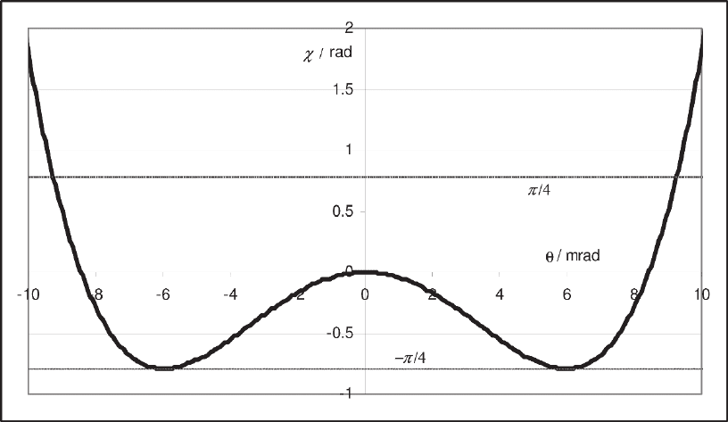
Once the peak-to-peak phase change of the rays converging to form
the probe is greater than π/2, there will be an element of destructive
interference, which we wish to avoid to form a sharp probe. Equation
(2.2) is a quartic function, but we can use negative defocus (underfo-
cus) to minimize the excursion of χ beyond a peak-to-peak change of
π/2 over as wide a range of angles as possible (Figure 2–4). Beyond a
critical angle, α, we use a beam-limiting aperture, known as the objec-
tive aperture, to prevent the more aberrated rays contributing to
the probe. This aperture can be represented in the FFP by a two-
dimensional top-hat function, H
α
(K). Now we can defi ne a so-called
aperture function, A(K), that represents the complex wavefunction in the
FFP,
A(K) = H
α
(K)exp[iχ(K)] (2.4)
Finally we can compute the wave function of the probe at the sample,
or probe function, by taking the inverse Fourier transform of (2.4) to
give
PA i dRK KRK
()
=
()
−
()
∫
exp 2π ⋅
(2.5)
To express the ability of the STEM to move the probe over the sample,
we can include a shift term in (2.5) to give
PAi idRR K KR KR K−
()
=
()
−
()()
0
∫
exp exp22
0
ππ⋅⋅
(2.6)
Figure 2–4. The aberration phase shift, χ, in the front-focal, or aperture, plane plotted as a function
of convergence angle, θ, for an accelerating voltage of 200 kV, C
S
= 1 mm and defocus z = −35.5 nm. The
darker lines indicate the π/4 limits giving a peak-to-peak variation of π/2.
72
Moving the probe is therefore equivalent to adding a linear ramp to
the phase variation across the FFP.
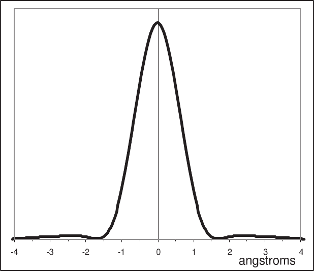
The intensity of the probe function is found by taking the modulus
squared of P(R), as is plotted for some typical values in Figure 2–5 Note
that this so-called diffraction limited probe has subsidiary maxima some-
times known as Airy rings, as would be expected from the use of an
aperture with a sharp cut-off. These subsidiary maxima can result in
weak features observed in images (see Section 5.3) that are image arti-
facts and not related to the specimen structure.
Let us examine the defocus and aperture size that should be used to
provide an optimally small probe. Different ways of measuring probe
size lead to various criteria for determining the optimal defocus (see, for
example, Mory et al., 1987), but they all lead to similar results. We can
again use the criterion of constraining the excursions of χ so that they
are no more than π/4 away from zero. For a given objective lens spherical
aberration, the optimal defocus is then given by
z = −0.71λ
1/2
C
S
1/2
(2.7)
allowing an objective aperture with radius
α = 1.3λ
1/4
C
S
−1/4
(2.8)
to be used. A useful measure of STEM resolution is the full-width at
half-maximum (FWHM) of the probe intensity profi le. At optimum
Figure 2–5. The intensity of a diffraction-limited STEM probe for the illumi-
nation conditions given in Figure 2–4. An objective aperture of radius 9.3 mrad
has been used.
Peter D. Nellist
Chapter 2 Scanning Transmission Electron Microscopy 73
defocus and with the correct aperture size, the probe FWHM is given
by
d = 0.4λ
3/4
C
S
1/4
(2.9)
Note that the use of increased underfocusing can lead to a reduction in
the probe FWHM at the expense of increased intensity in the subsidiary
maxima, thereby reducing the useful current in the central maximum
and leading to image artifacts. Along with other ways of quoting resolu-
tion, the FWHM must be interpreted carefully in terms of the image
resolution.
3. Coherent CBED and Ronchigrams
Most STEM detectors are located beyond the specimen and detect the
electron intensity in the far fi eld. To interpret STEM images, it is there-
fore fi rst necessary to understand the intensity found in the far fi eld.
In combination CTEM/STEM instruments, the far-fi eld intensity can
be observed on the fl uorescent screen at the bottom of the column
when the instrument is operated in STEM mode with the lower column
set to diffraction mode. In dedicated STEM instruments it is usual to
have a camera consisting of a scintillator coupled to a CCD array in
order to observe this intensity.
In conventional electron diffraction, a sample is illuminated with a
highly parallelized plane wave illumination. Electron scattering occurs,
and the intensity observed in the far fi eld is given by the modulus
squared of the Fourier transform of the wavefunction, y (R), at the exit
surface of the sample,
IidKK R KRR
()
=
()
=
()
[]
∫
Ψ
2
2
2ψπexp ⋅
(3.1)
The scattering wavevector in the detector plane, K, is related to the
scattering angle, q, by
K =
θ
λ
(3.2)
A detailed discussion of electron diffraction is in general beyond the
scope of this text, but the reader is referred to the many excellent text-
books on this subject (Hirsch et al., 1977; Cowley, 1990, 1992). In STEM,
the sample is illuminated by a probe that is formed from a collapsing
convergent spherical wavefront. The electron diffraction pattern is
therefore broadened by the range of illumination angles in the conver-
gent beam. In the case of a crystalline sample where one might expect
to observe diffracted Bragg spots, in the STEM the spots are broadened
into discs that may even overlap with their neighbors. Such a pattern
is known as a convergent beam electron diffraction (CBED) or micro-
diffraction pattern because the convergent beam leads to a small illu-
mination spot. See Spence and Zuo (1992) for a textbook covering
aspects of microdiffraction and CBED and Cowley (1978) for a review
of microdiffraction.
74
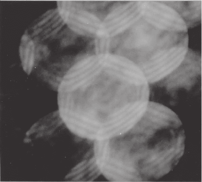
3.1 Ronchigrams of Crystalline Materials
If the electron source image at the sample is much smaller than the
diffraction limited probe, then the convergent beam forming the probe
can be regarded as being coherent. A crystalline sample diffracts elec-
trons into discrete Bragg beams, and in a STEM these are broadened to
give discs. The high coherence of the beam means that if the discs
overlap then interference features can be seen, such as the fringes in
Figure 2–6. Such coherent CBED patterns are also known as coherent
microdiffraction patterns or even nanodiffraction patterns. Their obser-
vation in the STEM has been described extensively by Cowley (1979b,
1981) and Cowley and Disko (1980) and reviewed by Spence (1992).
To understand the form of these interference fringes, let us fi rst
consider a thin crystalline sample that can be described by a simple
transmittance function, φ(R). The exit-surface wavefunction will be
given by,
y (R, R
0
) = P(R − R
0
)f(R) (3.3)
Where R
0
represents the probe position. Because Eq. 3.3 is a product of
two functions, taking its Fourier transform [inserting into Eq. (3.1)]
results in a convolution between the Fourier transform of P(R) and the
Fourier transform of φ (R). Taking the Fourier transform of P(R), from
Eq. (2.5) simply gives A(K). For a crystalline sample, the Fourier trans-
form of φ (R) will consist of discrete Dirac δ-functions, which correspond
to the Bragg spots, at values of K corresponding to the reciprocal lattice
points. We can therefore write the far fi eld wavefunction, Ψ(K), as a sum
of multiple aperture functions centered on the Bragg spots,
K g Kg R
0 0
2
( )
=−
()
−
()
[]
∑
φπ
g
g
Aiexp
i
(3.4)
Figure 2–6. A coherent CBED pattern of Si<110>. Note the interference fringes
in the overlap region that show that the probe is defocused from the sample.
Ψ K, R
Peter D. Nellist