Hennessy John L., Patterson David A. Computer Architecture
Подождите немного. Документ загружается.

22 ■ Chapter One Fundamentals of Computer Design
The number of dies per wafer is approximately the area of the wafer divided
by the area of the die. It can be more accurately estimated by
The first term is the ratio of wafer area (πr
2
) to die area. The second compensates
for the “square peg in a round hole” problem—rectangular dies near the periph-
ery of round wafers. Dividing the circumference (πd ) by the diagonal of a square
die is approximately the number of dies along the edge.
Example Find the number of dies per 300 mm (30 cm) wafer for a die that is 1.5 cm on a
side.
Answer The die area is 2.25 cm
2
. Thus
However, this only gives the maximum number of dies per wafer. The critical
question is: What is the fraction of good dies on a wafer number, or the die yield?
A simple model of integrated circuit yield, which assumes that defects are ran-
domly distributed over the wafer and that yield is inversely proportional to the
complexity of the fabrication process, leads to the following:
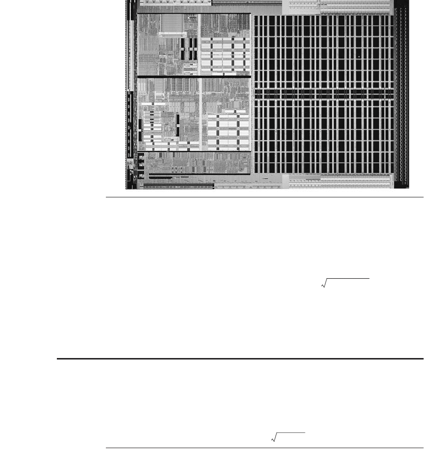
Figure 1.11 Photograph of an AMD Opteron microprocessor die. (Courtesy AMD.)
Dies per wafer
π Wafer diameter/2()
2
×
Die area
-----------------------------------------------------------=
–
π
Wafer diameter
×
2 Die area
×
-----------------------------------------------
Dies per wafer
π 30 2⁄()
2
×
2.25
------------------------------=
–
π
30
×
2 2.25
×
------------------------
706.9
2.25
-------------
–
94.2
2.12
----------
270==
Die yield Wafer yield 1
Defects per unit area Die area×
α
----------------------------------------------------------------------------+
–α
×=
1.6 Trends in Cost
■
23
The formula is an empirical model developed by looking at the yield of many
manufacturing lines.
Wafer yield
accounts for wafers that are completely bad and
so need not be tested. For simplicity, we’ll just assume the wafer yield is 100%.
Defects per unit area is a measure of the random manufacturing defects that
occur. In 2006, these value is typically 0.4 defects per square centimeter for
90 nm, as it depends on the maturity of the process (recall the learning curve,
mentioned earlier). Lastly,
α
is a parameter that corresponds roughly to the
number of critical masking levels, a measure of manufacturing complexity. For
multilevel metal CMOS processes in 2006, a good estimate is
α
= 4.0.
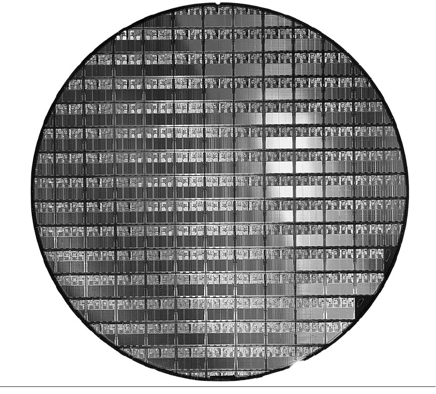
Figure 1.12
This 300mm wafer contains 117 AMD Opteron chips implemented in a 90 nm process.
(Courtesy
AMD.)

24
■
Chapter One
Fundamentals of Computer Design
Example
Find the die yield for dies that are 1.5 cm on a side and 1.0 cm on a side, assum-
ing a defect density of 0.4 per cm
2
and
α
is 4.
Answer
The total die areas are 2.25 cm
2
and 1.00 cm
2
. For the larger die, the yield is
For the smaller die, it is
That is, less than half of all the large die are good but more than two-thirds of the
small die are good.
The bottom line is the number of good dies per wafer, which comes from
multiplying dies per wafer by die yield to incorporate the effects of defects. The
examples above predict about 120 good 2.25 cm
2
dies from the 300 mm wafer
and 435 good 1.00 cm
2
dies. Many 32-bit and 64-bit microprocessors in a mod-
ern 90 nm technology fall between these two sizes. Low-end embedded 32-bit
processors are sometimes as small as 0.25 cm
2
, and processors used for embed-
ded control (in printers, automobiles, etc.) are often less than 0.1 cm
2
.
Given the tremendous price pressures on commodity products such as
DRAM and SRAM, designers have included redundancy as a way to raise yield.
For a number of years, DRAMs have regularly included some redundant memory
cells, so that a certain number of flaws can be accommodated. Designers have
used similar techniques in both standard SRAMs and in large SRAM arrays used
for caches within microprocessors. Obviously, the presence of redundant entries
can be used to boost the yield significantly.
Processing of a 300 mm (12-inch) diameter wafer in a leading-edge technol-
ogy costs between $5000 and $6000 in 2006. Assuming a processed wafer cost of
$5500, the cost of the 1.00 cm
2
die would be around $13, but the cost per die of
the 2.25 cm
2
die would be about $46, or almost four times the cost for a die that
is a little over twice as large.
What should a computer designer remember about chip costs? The manufac-
turing process dictates the wafer cost, wafer yield, and defects per unit area, so
the sole control of the designer is die area. In practice, because the number of
defects per unit area is small, the number of good dies per wafer, and hence the
cost per die, grows roughly as the square of the die area. The computer designer
affects die size, and hence cost, both by what functions are included on or
excluded from the die and by the number of I/O pins.
Before we have a part that is ready for use in a computer, the die must be
tested (to separate the good dies from the bad), packaged, and tested again after
packaging. These steps all add significant costs.
The above analysis has focused on the variable costs of producing a func-
tional die, which is appropriate for high-volume integrated circuits. There is,
however, one very important part of the fixed cost that can significantly affect the
Die yield 1
0.4 2.25×
4.0
------------------------+
4–
0.44==
Die yield 1
0.4 1.00×
4.0
------------------------+
4–
0.68==

1.7 Dependability ■ 25
cost of an integrated circuit for low volumes (less than 1 million parts), namely,
the cost of a mask set. Each step in the integrated circuit process requires a sepa-
rate mask. Thus, for modern high-density fabrication processes with four to six
metal layers, mask costs exceed $1 million. Obviously, this large fixed cost
affects the cost of prototyping and debugging runs and, for small-volume produc-
tion, can be a significant part of the production cost. Since mask costs are likely
to continue to increase, designers may incorporate reconfigurable logic to
enhance the flexibility of a part, or choose to use gate arrays (which have fewer
custom mask levels) and thus reduce the cost implications of masks.
Cost versus Price
With the commoditization of the computers, the margin between the cost to the
manufacture a product and the price the product sells for has been shrinking.
Those margins pay for a company’s research and development (R&D), market-
ing, sales, manufacturing equipment maintenance, building rental, cost of financ-
ing, pretax profits, and taxes. Many engineers are surprised to find that most
companies spend only 4% (in the commodity PC business) to 12% (in the high-
end server business) of their income on R&D, which includes all engineering.
Historically, integrated circuits were one of the most reliable components of a
computer. Although their pins may be vulnerable, and faults may occur over
communication channels, the error rate inside the chip was very low. That con-
ventional wisdom is changing as we head to feature sizes of 65 nm and smaller,
as both transient faults and permanent faults will become more commonplace, so
architects must design systems to cope with these challenges. This section gives
an quick overview of the issues in dependability, leaving the official definition of
the terms and approaches to Section 6.3.
Computers are designed and constructed at different layers of abstraction. We
can descend recursively down through a computer seeing components enlarge
themselves to full subsystems until we run into individual transistors. Although
some faults are widespread, like the loss of power, many can be limited to a sin-
gle component in a module. Thus, utter failure of a module at one level may be
considered merely a component error in a higher-level module. This distinction is
helpful in trying to find ways to build dependable computers.
One difficult question is deciding when a system is operating properly. This
philosophical point became concrete with the popularity of Internet services.
Infrastructure providers started offering Service Level Agreements (SLA) or
Service Level Objectives (SLO) to guarantee that their networking or power ser-
vice would be dependable. For example, they would pay the customer a penalty if
they did not meet an agreement more than some hours per month. Thus, an SLA
could be used to decide whether the system was up or down.
1.7 Dependability

26 ■ Chapter One Fundamentals of Computer Design
Systems alternate between two states of service with respect to an SLA:
1. Service accomplishment, where the service is delivered as specified
2. Service interruption, where the delivered service is different from the SLA
Transitions between these two states are caused by failures (from state 1 to state
2) or restorations (2 to 1). Quantifying these transitions leads to the two main
measures of dependability:
■ Module reliability is a measure of the continuous service accomplishment (or,
equivalently, of the time to failure) from a reference initial instant. Hence, the
mean time to failure (MTTF) is a reliability measure. The reciprocal of
MTTF is a rate of failures, generally reported as failures per billion hours of
operation, or FIT (for failures in time).Thus, an MTTF of 1,000,000 hours
equals 10
9
⁄10
6
or 1000 FIT. Service interruption is measured as mean time to
repair (MTTR). Mean time between failures (MTBF) is simply the sum of
MTTF + MTTR. Although MTBF is widely used, MTTF is often the more
appropriate term. If a collection of modules have exponentially distributed
lifetimes—meaning that the age of a module is not important in probability of
failure—the overall failure rate of the collection is the sum of the failure rates
of the modules.
■ Module availability is a measure of the service accomplishment with respect
to the alternation between the two states of accomplishment and interruption.
For nonredundant systems with repair, module availability is
Note that reliability and availability are now quantifiable metrics, rather than syn-
onyms for dependability. From these definitions, we can estimate reliability of a
system quantitatively if we make some assumptions about the reliability of com-
ponents and that failures are independent.
Example Assume a disk subsystem with the following components and MTTF:
■ 10 disks, each rated at 1,000,000-hour MTTF
■ 1 SCSI controller, 500,000-hour MTTF
■ 1 power supply, 200,000-hour MTTF
■ 1 fan, 200,000-hour MTTF
■ 1 SCSI cable, 1,000,000-hour MTTF
Using the simplifying assumptions that the lifetimes are exponentially distributed
and that failures are independent, compute the MTTF of the system as a whole.
Module availability
MTTF
MTTF MTTR+()
-------------------------------------------=

1.7 Dependability ■ 27
Answer The sum of the failure rates is
or 23,000 FIT. The MTTF for the system is just the inverse of the failure rate:
or just under 5 years.
The primary way to cope with failure is redundancy, either in time (repeat the
operation to see if it still is erroneous) or in resources (have other components to
take over from the one that failed). Once the component is replaced and the sys-
tem fully repaired, the dependability of the system is assumed to be as good as
new. Let’s quantify the benefits of redundancy with an example.
Example Disk subsystems often have redundant power supplies to improve dependability.
Using the components and MTTFs from above, calculate the reliability of a
redundant power supply. Assume one power supply is sufficient to run the disk
subsystem and that we are adding one redundant power supply.
Answer We need a formula to show what to expect when we can tolerate a failure and still
provide service. To simplify the calculations, we assume that the lifetimes of the
components are exponentially distributed and that there is no dependency
between the component failures. MTTF for our redundant power supplies is the
mean time until one power supply fails divided by the chance that the other will
fail before the first one is replaced. Thus, if the chance of a second failure before
repair is small, then MTTF of the pair is large.
Since we have two power supplies and independent failures, the mean time
until one disk fails is MTTF
power supply
⁄2. A good approximation of the proba-
bility of a second failure is MTTR over the mean time until the other power
supply fails. Hence, a reasonable approximation for a redundant pair of power
supplies is
Using the MTTF numbers above, if we assume it takes on average 24 hours for a
human operator to notice that a power supply has failed and replace it, the reli-
ability of the fault tolerant pair of power supplies is
making the pair about 4150 times more reliable than a single power supply.
Failure rate
system
10
1
1,000,000
------------------------
1
500,000
-------------------+×
1
200,000
-------------------
1
200,000
-------------------
1
1,000,000
------------------------+++=
102551++++
1,000,000
hours
-------------------------------------------
23
1,000,000
------------------------
23,000
1,000,000,000
hours
--------------------------------------------------===
MTTF
system
1
Failure rate
system
----------------------------------------
1,000,000,000
hours
23,000
--------------------------------------------------
43,500 hours===
MTTF
power supply pair
MTTF
power supply
2⁄
MTTR
power supply
MTTF
power supply
------------------------------------------
------------------------------------------------
MTTF
power supply
2
2⁄
MTTR
power supply
------------------------------------------------
MTTF
power supply
2
2 MTTR
power supply
×
---------------------------------------------------===
MTTF
power supply pair
MTTF
power supply
2
2 MTTR
power supply
×
---------------------------------------------------
200,000
2
224×
----------------------
830,000,000≅==

28
■
Chapter One
Fundamentals of Computer Design
Having quantified the cost, power, and dependability of computer technology, we
are ready to quantify performance.
When we say one computer is faster than another is, what do we mean? The user
of a desktop computer may say a computer is faster when a program runs in less
time, while an Amazon.com administrator may say a computer is faster when it
completes more transactions per hour. The computer user is interested in reduc-
ing
response time
—the time between the start and the completion of an event—
also referred to as
execution time
. The administrator of a large data processing
center may be interested in increasing
throughput
—the total amount of work
done in a given time.
In comparing design alternatives, we often want to relate the performance of
two different computers, say, X and Y. The phrase “X is faster than Y” is used
here to mean that the response time or execution time is lower on X than on Y for
the given task. In particular, “X is
n
times faster than Y” will mean
=
Since execution time is the reciprocal of performance, the following relationship
holds:
n
=
=
=
The phrase “the throughput of X is 1.3 times higher than Y” signifies here
that the number of tasks completed per unit time on computer X is 1.3 times the
number completed on Y.
Unfortunately, time is not always the metric quoted in comparing the perfor-
mance of computers. Our position is that the only consistent and reliable measure
of performance is the execution time of real programs, and that all proposed
alternatives to time as the metric or to real programs as the items measured have
eventually led to misleading claims or even mistakes in computer design.
Even execution time can be defined in different ways depending on what we
count. The most straightforward definition of time is called wall-clock time,
response time, or elapsed time, which is the latency to complete a task, including
disk accesses, memory accesses, input/output activities, operating system over-
head—everything. With multiprogramming, the processor works on another pro-
gram while waiting for I/O and may not necessarily minimize the elapsed time of
one program. Hence, we need a term to consider this activity. CPU time recog-
nizes this distinction and means the time the processor is computing, not includ-
1.8 Measuring, Reporting, and Summarizing Performance
Execution time
Y
Execution time
X
----------------------------------------
n
Execution time
Y
Execution time
X
----------------------------------------
1
Performance
Y
----------------------------------
1
Performance
X
----------------------------------
----------------------------------
Performance
X
Performance
Y
----------------------------------
1.8 Measuring, Reporting, and Summarizing Performance ■ 29
ing the time waiting for I/O or running other programs. (Clearly, the response
time seen by the user is the elapsed time of the program, not the CPU time.)
Computer users who routinely run the same programs would be the perfect
candidates to evaluate a new computer. To evaluate a new system the users would
simply compare the execution time of their workloads—the mixture of programs
and operating system commands that users run on a computer. Few are in this
happy situation, however. Most must rely on other methods to evaluate comput-
ers, and often other evaluators, hoping that these methods will predict per-
formance for their usage of the new computer.
Benchmarks
The best choice of benchmarks to measure performance are real applications,
such as a compiler. Attempts at running programs that are much simpler than a
real application have led to performance pitfalls. Examples include
■ kernels, which are small, key pieces of real applications;
■ toy programs, which are 100-line programs from beginning programming
assignments, such as quicksort; and
■ synthetic benchmarks, which are fake programs invented to try to match the
profile and behavior of real applications, such as Dhrystone.
All three are discredited today, usually because the compiler writer and architect
can conspire to make the computer appear faster on these stand-in programs than
on real applications.
Another issue is the conditions under which the benchmarks are run. One
way to improve the performance of a benchmark has been with benchmark-
specific flags; these flags often caused transformations that would be illegal on
many programs or would slow down performance on others. To restrict this pro-
cess and increase the significance of the results, benchmark developers often
require the vendor to use one compiler and one set of flags for all the programs in
the same language (C or FORTRAN). In addition to the question of compiler
flags, another question is whether source code modifications are allowed. There
are three different approaches to addressing this question:
1. No source code modifications are allowed.
2. Source code modifications are allowed, but are essentially impossible. For
example, database benchmarks rely on standard database programs that are
tens of millions of lines of code. The database companies are highly unlikely
to make changes to enhance the performance for one particular computer.
3. Source modifications are allowed, as long as the modified version produces
the same output.
The key issue that benchmark designers face in deciding to allow modification of
the source is whether such modifications will reflect real practice and provide
30 ■ Chapter One Fundamentals of Computer Design
useful insight to users, or whether such modifications simply reduce the accuracy
of the benchmarks as predictors of real performance.
To overcome the danger of placing too many eggs in one basket, collections
of benchmark applications, called benchmark suites, are a popular measure of
performance of processors with a variety of applications. Of course, such suites
are only as good as the constituent individual benchmarks. Nonetheless, a key
advantage of such suites is that the weakness of any one benchmark is lessened
by the presence of the other benchmarks. The goal of a benchmark suite is that it
will characterize the relative performance of two computers, particularly for pro-
grams not in the suite that customers are likely to run.
As a cautionary example, the EDN Embedded Microprocessor Benchmark
Consortium (or EEMBC, pronounced “embassy”) is a set of 41 kernels used to
predict performance of different embedded applications: automotive/industrial,
consumer, networking, office automation, and telecommunications. EEMBC
reports unmodified performance and “full fury” performance, where almost any-
thing goes. Because they use kernels, and because of the reporting options,
EEMBC does not have the reputation of being a good predictor of relative perfor-
mance of different embedded computers in the field. The synthetic program
Dhrystone, which EEMBC was trying to replace, is still reported in some embed-
ded circles.
One of the most successful attempts to create standardized benchmark appli-
cation suites has been the SPEC (Standard Performance Evaluation Corporation),
which had its roots in the late 1980s efforts to deliver better benchmarks for
workstations. Just as the computer industry has evolved over time, so has the
need for different benchmark suites, and there are now SPEC benchmarks to
cover different application classes. All the SPEC benchmark suites and their
reported results are found at www.spec.org.
Although we focus our discussion on the SPEC benchmarks in many of the
following sections, there are also many benchmarks developed for PCs running
the Windows operating system.
Desktop Benchmarks
Desktop benchmarks divide into two broad classes: processor-intensive bench-
marks and graphics-intensive benchmarks, although many graphics benchmarks
include intensive processor activity. SPEC originally created a benchmark set
focusing on processor performance (initially called SPEC89), which has evolved
into its fifth generation: SPEC CPU2006, which follows SPEC2000, SPEC95
SPEC92, and SPEC89. SPEC CPU2006 consists of a set of 12 integer bench-
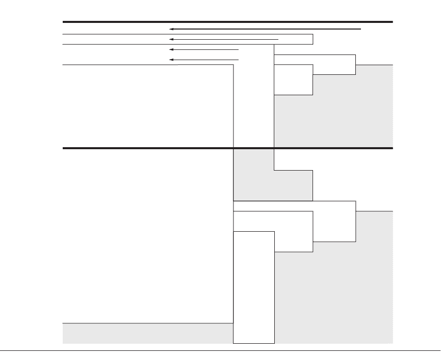
marks (CINT2006) and 17 floating-point benchmarks (CFP2006). Figure 1.13
describes the current SPEC benchmarks and their ancestry.
SPEC benchmarks are real programs modified to be portable and to minimize
the effect of I/O on performance. The integer benchmarks vary from part of a C
compiler to a chess program to a quantum computer simulation. The floating-
point benchmarks include structured grid codes for finite element modeling, par-
1.8 Measuring, Reporting, and Summarizing Performance ■ 31
ticle method codes for molecular dynamics, and sparse linear algebra codes for
fluid dynamics. The SPEC CPU suite is useful for processor benchmarking for
both desktop systems and single-processor servers. We will see data on many of
these programs throughout this text.
Figure 1.13 SPEC2006 programs and the evolution of the SPEC benchmarks over time, with integer programs
above the line and floating-point programs below the line. Of the 12 SPEC2006 integer programs, 9 are written in
C, and the rest in C++. For the floating-point programs the split is 6 in FORTRAN, 4 in C++, 3 in C, and 4 in mixed C
and Fortran. The figure shows all 70 of the programs in the 1989, 1992, 1995, 2000, and 2006 releases. The bench-
mark descriptions on the left are for SPEC2006 only and do not apply to earlier ones. Programs in the same row from
different generations of SPEC are generally not related; for example, fpppp is not a CFD code like bwaves. Gcc is the
senior citizen of the group. Only 3 integer programs and 3 floating-point programs survived three or more genera-
tions. Note that all the floating-point programs are new for SPEC2006. Although a few are carried over from genera-
tion to generation, the version of the program changes and either the input or the size of the benchmark is often
changed to increase its running time and to avoid perturbation in measurement or domination of the execution
time by some factor other than CPU time.
SPEC2006 benchmark description
GNU C compiler
Interpreted string processing
Combinatorial optimization
Block-sorting compression
Go game (AI)
Video compression
Games/path finding
Search gene sequence
Quantum computer simulation
Discrete event simulation library
Chess game (AI)
XML parsing
CFD/blast waves
Numerical relativity
Finite element code
Differential equation solver framework
Quantum chemistry
EM solver (freq/time domain)
Scalable molecular dynamics (~NAMD)
Lattice Boltzman method (fluid/air flow)
Large eddie simulation/turbulent CFD
Lattice quantum chromodynamics
Molecular dynamics
Image ray tracing
Spare linear algebra
Speech recognition
Quantum chemistry/object oriented
Weather research and forecasting
Magneto hydrodynamics (astrophysics)
gcc
espresso
li
eqntott
perl
mcf
bzip2
vortex
gzip
eon
twolf
vortex
vpr
crafty
parser
wupwise
apply
galgel
mesa
art
equake
facerec
ammp
lucas
fma3d
sixtrack
apsi
mgrid
applu
turb3d
swim
hydro2d
su2cor
wave5
fpppp
tomcatv
doduc
nasa7
spice
matrix300
go
h264avc
astar
hmmer
libquantum
omnetpp
sjeng
xalancbmk
bwaves
cactusADM
calculix
dealll
gamess
GemsFDTD
gromacs
lbm
LESlie3d
milc
namd
povray
soplex
sphinx3
tonto
wrf
zeusmp
SPEC89SPEC95
Benchmark name by SPEC generation
SPEC92SPEC2000SPEC2006
go
ijpeg
m88ksim
compress
sc