Lallart M. (ed.) Ferroelectrics - Physical Effects
Подождите немного. Документ загружается.


Localized States in Narrow-Gap Ferroelectric-Semiconductor PbSnTe:
Injection Currents, IR and THz Photosensitivity, Magnetic Field Effects
539
In the experiment (see Figure 9), the magnetic field was rotated through the angle 360°
during 8 minutes so that at each angle a quasi-equilibrium magnitude of the current could
establish. Both dependences in Figure 9 show no pronounced angular symmetry.
Nonetheless, it is seen from Figure 9 a that two minima of the current lie in the vicinity of
the angles 0° and 180°, for which the vector
B was normal to the substrate. The position of
the most pronounced maximum is near the angle 270
o
, at which the field B was normal to
the substrate. Yet, the other «local» maximum, located at 120
o
, is observed rather far from
the angle 90°, at which the vector
B is also parallel to the substrate.
In Figure 9 b the angle between the two maxima is close to 240°, with the «main» minimum
being located at the middle point of the maxima with angular spacing of approximately 120°
from either maximum. In principle, this position of the three extrema correlates with the
orientation of the BaF
2
(111) substrate. Yet, the position of the second «local» minimum
shows no such regularity.
The behavior demonstrated by the current in a strong magnetic field also substantially
depends on the orientation of this field with respect to the electric-field vector and the
normal to the substrate, and it can appear nonmonotonic with variation of
B . Figure 10
shows the curves of relative current for mutual orientation 2 of the two fields (Fig. 7 a) at
various bias voltages. The maximum increase in current (over 200 times) was reached
approximately at B=1.3 T and at bias-voltage value U≈3 V, i.e. in the vicinity of the voltage
at which the effect in weak magnetic fields was also most pronounced (Fig. 8 a)).
Fig. 10. The ratio I(B)/I(B=0) versus magnetic-field strength. Here, the magnetic field and
the electric field are parallel to each other. Bias voltage U, V= 2.66 (1); 2.77 (2); 2.93 (3); 3.1
(4); 4.05 (5); 5.2 (6).
4.3 Discussion
Consider possible factors causing the variation of the electric current under the action of a
constant magnetic field. In Section 3 it was shown that at helium temperatures the
behavior of current-voltage characteristics of PbSnTe:In films obeys the theory of space-
charge-limited current in the presence of electron traps. In the case under discussion, the
change of current-voltage characteristics in a magnetic field should be attributed to a
change of dielectric permittivity (polarizability) of the medium providing that such a
change does take place.

Ferroelectrics – Physical Effects
540
Consider possible change of the effective value of ε as a factor causing variation of the
current-voltage curves. Assuming variation of dielectric permittivity by ±30%, we
performed numerical calculations of the current-voltage characteristics; the calculated data
are shown in Figure 11, curves 1, 2, and 3, together with experimental data. As it is seen
from the figure, a good agreement between the calculated and experimental data is
observed.
Fig. 11. Current-voltage characteristics of a PbSnTe:In sample at Т=4.2 K. Symbols –
experimental data; solid lines – calculated data. 1 and squares – В=0, 2 and circles – В = 4 T,
orientation 2 in Figure 7 a, 3 and triangles – В = 1.33 T, orientation 2 in Figre 7 a.
Of course, here we do not mean the variation of ε under the action of magnetic field. The
magnetic field can alter the current direction by the Hall angle, which in PbSnTe:In can be
rather large because of a high value of charge-carrier mobility. In turn, it is the polarizability
of the medium in the direction of current that will affect the space-charge magnitude and
the current strength, thus making the latter quantities dependent on the direction and
strength of magnetic field. If we assume that precisely this factor defines the anisotropic
effects in magnetic field, then the dependence of ε on field orientation can also be expected
to take place without the magnetic field. To clarify this point, at B=0 we examined the
angular dependence of ε and the shape of current-voltage characteristics of structures S2
under conditions with space-charge-controlled limitation of injection current at various
orientations of the external electric field.
Fig. 12. Dependence of ε on gap orientation in structure S2. The wide arrows indicate the
approximate angular position of the maximal and minimal values of ε.

Localized States in Narrow-Gap Ferroelectric-Semiconductor PbSnTe:
Injection Currents, IR and THz Photosensitivity, Magnetic Field Effects
541
The angular dependence of ε was measured on an experimental structure shown in Figure 7
b. The experimental data measured at frequency f=10
4
Hz are shown in Fig. 12. The
dependence shows distinct minima and maxima whose presence in the dependence can be
identified by 2 to 4 experimental points within each feature.
The experimentally revealed dependence of ε on electrical-field orientation explains the
observed transformation of current-voltage characteristics in a magnetic field. Yet, factors
causing the variation of ε need further discussion. At room temperature PbSnTe has a face-
centered cubic lattice with the NaCl structure (space group
5
3
h
OFmm
). As a result of the
ferroelectric phase transition, the lattice becomes rhombohedric, involving equivalent [111]
spontaneous-polarization axes of «free» crystal. As far as our knowledge goes, so far no data
on the dependence of static dielectric permittivity on crystallographic direction in PbSnTe:In
have been reported; on the other hand, for thoroughly studied ferroelectrics, such as, for
instance, barium titanate, the dielectric-permittivity values measured along directions [010]
and [001] form a tensor, whose components in some temperature range can differ by ten to
hundred times (Vinogradov & Kucherenko, 1991). The axis along which spontaneous
polarization in PbSnTe:In occurs seems to be not parallel to the surface normal, being
instead one of the three equivalent type [111] axes directed at an angle to the substrate. The
projections of those axes onto the substrate plane are separated with 60° angles. One factor
making the indicated three axes nonequivalent on large scale and leading to spontaneous
polarization along one of those axes can be some deviation from singularity that inevitably
occurs in preparation of BaF
2
(111) substrates.
In principle, if spontaneous polarization along one of the three equivalent type-[111] axes
does occur, a 60- or 120-deg angular symmetry of the effect in the substrate plane can be
expected; such a symmetry is probably manifested in Fig. 9 b. Simultaneously, geometric
factors, such as, for instance, a large length of the inter-electrode gap, a small film thickness,
and also a multi-domain structure of the film, could also induce distortions into this type of
symmetry.
Of course, the model discussed above is a simplified model. In particular, the experimental
current-voltage characteristic in substrate-normal magnetic field in Figure 11 and the
calculated current-voltage curve can be brought in agreement assuming 30% variation of ε,
while measured angular variations of ε are restricted to within 20%. Finally, the model
ignores the influence of possible multi-domain structure of PbSnTe:In films on the shape of
current-voltage curves, which may appear rather substantial.
4.4 Summary
The giant (up to 10
4
) change in the electric current in Pb
1-x
Sn
x
Te:In films placed in a
magnetic field can be explained within the frame of the following model. The polarizability
of PbSnTe:In films in ferroelectric phase at T=4.2 K is anisotropic and, in such films, there
exists a preferential direction of spontaneous polarization in which the static dielectric
permittivity ε is maximal. The latter assumption is qualitatively corroborated by
experimental data on anisotropic properties of the films in zero magnetic field. Since the
measured currents are space-charge-limited injection currents, the magnitude of these
currents depends on the value of ε in the direction in which the current flows. It can
therefore be expected that a magnetic-field-induced change of current direction will alter the
magnitude of the current. The observed effect can be explained on the assumption that, on

Ferroelectrics – Physical Effects
542
the change of current direction, the voltage U
t
at which the traps in the film become filled
with electrons also undergoes a change in the magnetic field, because this voltage is
inversely proportional to ε. In a narrow interval of voltages around U
t
the electric current
increases by several orders. As a result, at a fixed bias voltage even a small change in ε in the
above interval will lead to a drastic change of the electric current, this change amounting in
the experiments to several orders. Within this model, the complex anisotropy displayed by
the effect also receives qualitative explanation. Namely, the magnetic-field-induced increase
or decrease of the electric current is defined by the mutual orientation of electric field,
magnetic field, spontaneous polarization, and the normal to substrate plane.
5. Photosensitivity of PbSnTe in the fundamental absorption band and
in THz spectral region
5.1 Photocurrent in the fundamental absorption band
It is known from literature (Emtage, 1976; Lishka et al., 1984) that the predominant
recombination mechanism in undoped PbSnTe samples is Auger recombination. Low
concentrations of electrons and holes in PbSnTe:In make the Auger recombination a less
probable process. In (Borodin et al., 1997b), it was found that in PbSnTe:In films a
satisfactory agreement between experimental and calculated data could be achieved on the
assumption that a predominant contribution was due to radiative recombination.
In calculating the photocurrent (Klimov & Shumsky, 2008), it was assumed that the Fermi
level under equilibrium conditions lay at the middle of the forbidden band, the
concentrations of electrons and holes were negligible, and the concentration of free electrons
was defined by the injection current. It was also assumed that there was just one trap level
in the material, available in a concentration 5·10
13
cm
-3
and located at energy 0.0065 eV
below the conduction-band bottom.
In the dark, in the PbSnTe:In bulk there is an uncompensated negative charge due to
electrons, and an injection current flows through the sample. In an illuminated material,
optically excited electrons recombine with holes, the role of equilibrium electron
concentration here being played by the sum of equilibrium and injected electrons. In
performing numerical calculations, the concentration of field-injected electrons in the
conduction band and the rate of optical generation of charge carriers were set separately.
The total concentration of free electrons defined the energy position of Fermi level and trap
occupation values under steady-state conditions. In calculating the Auger lifetime, for the
Auger recombination coefficient a value
η
n
=
η
p
=5⋅10
-26
cm
6
⋅s
-1
was adopted (Emtage, 1976).
The radiative lifetime was calculated based on the detailed balance principle (Rooesbroeck
& Shockley, 1954).
The temperature dependence of both, Auger and radiative, lifetimes at various contact
injection levels is shown in Figure 13 a. At helium temperatures, the chosen minimal total
concentration of equilibrium and field-injected electrons refers to the case of almost empty
traps, while the maximal total concentration of electrons, to almost completely filled traps
(Akimov et al., 2005).
Measurements showed that our PbSnTe:In films were dominated by radiative
recombination. Under monopolar electron injection, the hole concentration decreases with
increasing injected concentration of free electrons. Illumination produces additional
amounts of localized electrons and free holes. Capture of electrons at traps decreases the
rate of band-to-band recombination and increases the steady-state hole concentration, thus

Localized States in Narrow-Gap Ferroelectric-Semiconductor PbSnTe:
Injection Currents, IR and THz Photosensitivity, Magnetic Field Effects
543
increasing the photocurrent value. The calculated electron and hole components of the
photocurrent as functions of bias voltage are shown in Fig. 13 b.
(a) (b)
Fig. 13. Temperature-dependent radiative lifetime (a) and calculated dependences of the
photocurrent on bias voltage (b).
a - radiative (1-5) and Auger (6) lifetimes of holes at Δn
ph
=10
6
cm
-3
and n
0
+n
inj
= 10
6
, 10
8
, 10
10
,
10
12
, 10
14
(curves 1 – 6, respectively).
b - photocurrent component due to electrons (1), due to holes (2) , and the total current
(solid line 3) versus bias voltage at g
0
=10 cm
-3.
s
-1
.
The prevalence of the hole photocurrent component over an interval of bias voltages up to
the voltage at which the traps become filled with electrons is due to the fact that, because of
the electron capture at traps, the concentration of free holes here far exceeds the
concentration of free electrons. Under such conditions, the hole lifetime is defined by the net
concentration of electrons in the conduction band. With further increase of bias voltage, the
concentration of conduction-band electrons increases while the lifetime and concentration of
optically generated holes start decreasing. In the end, after all traps become filled with
electrons, the concentration of excess electrons becomes roughly equal to the concentration
of excess holes, and the lifetime of those holes, defined by the concentration of injected
electrons. Since the latter concentration is high, the lifetime is short, and the photocurrent is
weak.
An important outcome of the calculations is a prediction that until the onset of the regime
with completely filled traps the photocurrent should be due to holes.
It was shown experimentally (Klimov & Shumsky, 2008) that in weak fields a hole-type
conductivity was observed, with the Hall coefficient being almost independent of bias
voltage. In strong fields a current due to electrons is observed, with the Hall effect exhibiting
a strong dependence on bias voltage.
5.2 Photocurrent in the THz region
With the previously determined energy distribution of localized centers, the sensitivity of
PbSnTn to radiation in submillimeter spectral region due to electron excitation from a center
into the conduction band can be calculated (Klimov & Shumsky, 2009). A specific feature of
the photocurrent under conditions with space-charge-controlled limitation of current is a
strong dependence of photocurrent on the occupation of the local level, this occupation
Ferroelectrics – Physical Effects
544
being in turn dependent on the electron injection level, or bias voltage. This dependence is
expected to be manifested most sharply when the trap level lies far from the equilibrium
Fermi level. The steady-state concentration of optically generated electrons can be
calculated, in principle, similarly to calculations of impurity photoconductivity.
Fig. 14. Current-voltage characteristics of PbSnTe samples illuminated at laser-radiation
wavelengths 130 μm (curve 1 – calculated data; squares – experimental data) and 198 μm
(curve 2 – calculated data; triangles – experimental data).
Fig. 15. Spectral dependences of the photocurrent in a structure with an energy distribution
of states over the PbSnTe forbidden band shown in Fig. 4, Section 2. U=1.16 (1), 1.79 (2), 1.83
(3), 2.95 V.
The calculated photocurrent values in a sample illuminated with radiation at wavelengths
130 μm (hν=9.54 meV) and 198 μm (hν=6.26 meV) versus bias voltage are shown in Figure
14. The same figure shows the photocurrent values measured in our experiments at the
indicated wavelengths.
Figure demonstrates the difference between the curves of photocurrent versus bias voltage
for quantum energies hν=9.54 meV and 6.26 meV. In the former case, on increasing the bias
voltage from 0.7 V to 5 V the photocurrent varies over an interval of current values slightly
in excess of two orders. In the latter case, the photocurrent exhibits variation within the
same range of current values on increasing the bias voltage from 1.5 to 2.3 V, the
photocurrent growth here being much sharper. Qualitatively, such a behavior complies with
the one expected from the energy distribution of states in the forbidden band of PbSnTe.

Localized States in Narrow-Gap Ferroelectric-Semiconductor PbSnTe:
Injection Currents, IR and THz Photosensitivity, Magnetic Field Effects
545
Calculated values of spectral photosensitivity in a PbSnTe structure under various bias
voltages are shown in Fig. 15. It is seen that an increase in the injection level results in a
growth of the photocurrent throughout the whole spectral region, this growth being most
pronounced at wavelengths λ>200 μm.
5.3 Discussion
The experimental data obtained in our study of photoelectric properties of PbSnTe:In films,
and also performed calculations, allow the following conclusions to be drawn:
1.
On the passage to «dielectric state», the rate of recombination of optically excited charge
carriers becomes predominantly defined by the radiative lifetime, whose magnitude
depends on the field-injection level of electrons, on the values of trap parameters, and
on the optical injection level.
2.
Trapping of optically generated electrons at low field-injection levels leads to
prevalence of the photocurrent component due to holes, which on increasing the field-
injection level decreases due to recombination of optically excited holes. At high field-
injection levels, the photocurrent component due to electrons becomes prevailing. The
latter explains the photocurrent quenching by a voltage pulse.
3.
The calculated data have found confirmation in measurement of Hall effect in weakly
illuminated samples, whose conductivity varies from p-type conductivity at low field-
injection levels to n-type conductivity at high field-injection levels.
4.
The presence of localized electron traps distributed in energy over the PbSnTe
forbidden band may lead to non-exponential photocurrent decay, and also to some
other effects such as self-oscillations that were observed, among other things, in Hall
effect measurements of weakly illuminated samples.
5.
Our calculations of the photocurrent in THz region showed a good agreement with
experimental data. Excitation of electrons trapped at energy-distributed localized states
in the forbidden band of PbSnTe seems to be capable of providing a reasonable
explanation to the high sensitivity of PbSnTe:In films to radiation emitted by weakly
heated bodies.
6.
Dependence of photosensitivity spectrum in this spectral region on the occupation of
traps can be employed in the development of a THz radiation detector controlled by
bias voltage applied to the PbSnTe:In structure.
6. Oscillating transient currents in samples screened from background
radiation
6.1 Experimental results
Under conditions with screened background radiation at Т=4.2 K, we examined the
dynamics of injection currents in “dielectric” PbSnTe:In films of thickness 1÷1.5 μm grown
by molecular-beam epitaxy on (111) BaF
2
substrates. The specific resistance of the films at
Т=4.2K was
ρ
=10
10
÷10
12
Ohm·cm. A sample was cooled to Т=4.2 K at zero bias voltage, and
then a new voltage in the range U=2.5 to 6.0 V was applied to it to register the curve of
transient current. At each set value of bias voltage, measurements were repeated thrice.
After registration of the first curve (during 40-200 s), the applied voltage was removed from
the sample and, after the same time elapsed, the voltage was again applied to the sample to
register a second transient-current curve. Then, the sample was “warmed” to a temperature

Ferroelectrics – Physical Effects
546
of 30 K to be again cooled to 4.2 K. Afterwards, the same bias voltage was applied to the
sample to register a third transient-current curve.
Figure 16 a, b shows the curves of transient current for bias-voltage values U=2.5 V and
U=4.0 V. It is seen that the current in the second measurement was roughly the same as the
current at the end of the first measurement; this observation proves that the transition
process was over. In the third measurement, the curve of transient current closely followed
the curve obtained in the first measurement; the former curve is therefore not shown in the
figure. A characteristic feature of the relaxation process was involvement of self-oscillations
in the relaxation. The current decay is not monotonic, displaying instead an oscillating
behavior. The frequency and amplitude of the oscillations depended on the applied voltage
value.
a) b)
Fig. 16. The curves of transient current registered on application of a voltage step to the
sample. The bias voltages are U=2.5 V (a) and U=4.0 В (b). The inserts shows the curves of
transient current on an enlarged scale.
6.2 Discussion
It is a well-known fact that under certain conditions undamped oscillations can arise in
semiconductor structures whose current-voltage characteristics display curve portions with
negative differential resistance (NDR). Simultaneously, under certain combinations of
external parameters such as temperature, field strength, and illumination intensity, similar
self-oscillations were also observed in materials without NDR, for instance, in compensated
Si and Ge, and in PbSnTe:In (Akimov et al., 1993).
In applicable theories, the emergence of self-oscillations was related to the occurrence of
either trap recharging waves (Suris & Fuks, 1975) or recombination waves in the samples
(Bonch-Bruevich & Kalashnikov, 1965); however, in all cases a positive feedback, leading to
current growth, was necessary. Such a positive feedback can be ensured by an illumination
causing transitions of trapped electrons to the conduction band, collisional ionization of
excited electron traps, etc. For instance, according to (Bonch-Bruevich & Kalashnikov, 1965),
for emergence of self-oscillations in a unipolar semiconductor the concentration of free
charge carriers has to be controlled not only by trapping at one of the centers with a capture
cross-section dependent on field intensity, but also by optical generation of free carriers
from an impurity level of another type. In our experiments, measurements were carried out

Localized States in Narrow-Gap Ferroelectric-Semiconductor PbSnTe:
Injection Currents, IR and THz Photosensitivity, Magnetic Field Effects
547
under conditions with background radiation screening, so that the feedback was ensured by
some other mechanism.
Previously, we showed (Akimov et al.,
2005) that electron transport in semi-insulating
PbSnTe:In at helium temperatures cannot be treated without regard for monopolar injection of
electrons out of contacts and space-charge-controlled limitation of the current with capture of
electrons into localized centers in the forbidden band of PbSnTe. Such an approach has
allowed us to explain the shape of current-voltage curves, the high photosensitivity of PbSnTe
in the fundamental absorption band, and the emergence of photosignal during excitation of
the material in submillimeter band; additionally, an analysis of current-voltage characteristics
has allowed us to determine the energy spectrum of localized electron traps (Klimov &
Shumsky, 2009). The presence of electron traps and possible recharging of these traps may
have an influence on the transition processes. It should be noted that the experimentally
observed undamped current oscillations bear no relation to the self-oscillations considered in
(Suris & Fuks, 1975; Bonch-Bruevich & Kalashnikov, 1965); the former self-oscillations were
observed as an oscillating decay to a steady state after application of a voltage step to the
sample. This means that, here, the feedback mechanism, or the mechanism causing an increase
of electric current, gradually ceases its operation.
In (Klimov & Shumsky, 2001) we discussed the so-called “photodielectric effect”,
experimentally observed in PbSnTe:In, that consisted in a considerable (up to two orders)
increase of static dielectric permittivity in samples under illumination. This increase can be
related to a growth of electronic dielectric susceptibility observed in disordered
semiconductors with localization of electrons at discrete levels (Bonch-Bruevich,
1974).
The observed undamped current oscillations can be explained as follows. In the forbidden
band of a PbSnTe:In film, there is a quasi-continuous distribution of electron traps; in
subsequent discussion, we will treat this distribution by replacing it with a discrete-level set,
the levels within the set having different concentrations, energy positions, and electron
capture cross-sections. We assume that the steady-state Fermi level is located below the
i-th
center, and the temperature is sufficiently low for those centers at equilibrium to be empty,
for the concentration of conduction-band electrons to be negligible, and for the current
through sample to be limited by the space charge and by the trapping of injected electrons at
those centers.
On application of a voltage step, injection of an electron concentration
n
inj
=
ε
0
ε
s
U/(qL
2
) into
the sample takes place, where
0
ε
is the dielectric constant,
s
ε
is the static dielectric
permittivity of the sample, U is the bias voltage,
q is the electron charge, and L is the spacing
between the contacts. Consider the variation of the electron concentration in the conduction
band and at localized centers starting from a moment
0
M
t
τ
> , where the latter time is the
Maxwell relaxation time. We use an approximation that disregards the diffusion currents
and the spatial distribution of electrons over the sample length. Under this assumption, a
system of continuity equations with given concentrations and energies of centers can be
solved numerically.
Here, a situation may emerge in which a predominant fraction of conduction-band electrons
will be first captured by a center with a large capture cross-section, and then the electrons
from this center will be emitted into the conduction band to subsequently become trapped at
a next center, and so on. Since at an arbitrary time we have
(
)()
inj i
i
nt n m t=−
∑
, then the
time dependence of the current can be written as
Ferroelectrics – Physical Effects
548
() () ()
2
0
3
s
i
i
U
U
j
t
q
ntE
q
mt
L
L
εε μ
μμ
== −
∑
.
The above equation shows that the current will decrease in time exhibiting features
dependent on the effective time of electron capture into traps up to the establishment of a
steady state. Yet, as it follows from (Klimov & Shumsky, 2001), in PbSnTe:In there exist one
or several centers which, as they capture electrons, enhance the static dielectric permittivity
due to increased electronic dielectric susceptibility. In the latter case, the current is given by
() () ()
2
00
32
s
ii i
ii
UU
U
jt q m t m t
L
LqL
εεμ ε
μβ
⎡
⎤
⎢
⎥
=+ −
⎢
⎥
⎣
⎦
∑∑
, (1)
where
i
β
is the contribution to polarizability due to one electron captured at the i-th center.
An analysis of expression (1) shows that at the initial time (
t=t
0
) the current is defined by the
first term; at subsequent times, an increase or a decrease of the current is defined by the sign
of the bracketed expression. Thus, after application of the voltage step the system can come
into a steady state experiencing damped current oscillations. For damped current
oscillations to emerge, it is required that the expression in squared brackets would be
changing its sign as the centers with a longer time
i
CM
τ
get filled with electrons.
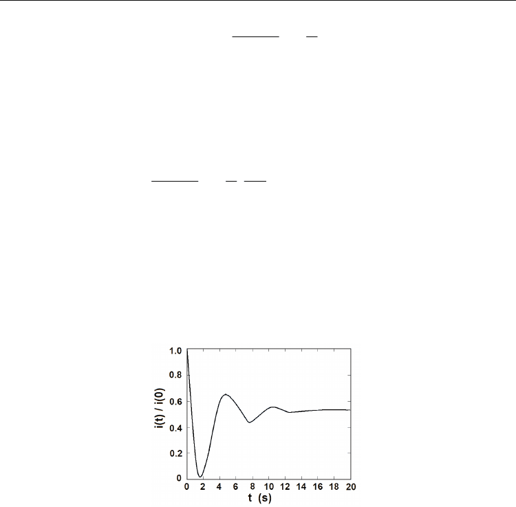
Fig. 17. Calculated current self-oscillations on application of a voltage step U=0.02 V to the
sample. The parameter values of the centers are indicated in the text.
The data obtained in numerical calculations of the ratio
j(t)/j(0) for the model with four
discrete levels belonging to centers making different contributions to dielectric susceptibility
on electron captures at those levels are shown in Figure 17. The values of trap parameters
were chosen rather arbitrarily; they were as follows: М
1
=1.8
.
10
12
cm
-3
, ΔЕ
М1
=4 meV,
γ
1
=1.8
.
10
-13
cm
3
/s, β
1
=0.5
.
10
-9
; М
2
=1.9
.
10
12
cm
-3
, ΔЕ
М2
=5 meV, γ
2
=6.6
.
10
-14
cm
3
/s, β
2
=0.8
.
10
-9
;
М
3
=3.0
.
10
12
cm
-3
, ΔЕ
М3
=6 meV, γ
3
=6.3
.
10
-15
cm
3
/s, β
3
=1.65
.
10
-9
; М
4
=5.8
.
10
12
cm
-3
, ΔЕ
М4
=8 meV,
γ
4
=2.0
.
10
-16
cm
3
/s, and β
4
=1.1
.
10
-9
. The numerical values of β
i
were chosen such that an
increase of current due to increased dielectric permittivity would occur when electrons were
getting trapped into the third center in terms of energy.
It is seen from Figure 17 that even involvement of a single such level can lead to damped
current oscillations in the trap charging and recharging process. Qualitatively, it is clear that,
with the injected electron concentration being much greater than the total concentration of