Lallart M. Ferroelectrics: Applications
Подождите немного. Документ загружается.

8
Fabrication and Study on One-Transistor-
Capacitor Structure of Nonvolatile Random
Access Memory TFT Devices Using
Ferroelectric Gated Oxide Film
Chien-Min Cheng, Kai-Huang Chen, Chun-Cheng Lin,
Ying-Chung Chen, Chih-Sheng Chen and Ping-Kuan Chang
Department of Electronics Engineering, Tung-Fang Design University,
Department of Electronic Engineering, Southern Taiwan University,
Department of Mathematics and Physics, Chinese Air Force Academy,
R.O.C.
1. Introduction
Recently, non-volatile and volatile memory devices such as static random access memory
(SRAM), dynamic random access memory (DRAM), Flash memory, EPROM and E
2
PROM
were very important for applications in conventional personal computer and micro-
processor, and performance efficiency of hardware improved by their low voltage, high
operation speed, and large storage capacity. The non-volatile memory devices were widely
investigated and discussed among these memory devices. Many kind of the non-volatile
memory device were ferroelectric random access memory (FeRAM), magnetron random
access memory (MRAM), and resist random access memory (RRAM) devices. Up to now,
the non-volatile ferroelectric random access memory (FeRAM) devices were attractive
because of their low coercive filed, large remnant polarization, and high operation speed
among various non-volatile access random memory devices [1].
The non-volatile FeRAM devices were limited by their relative larger one-transistor-one-
capacitor (1T-1C) size. Thus, one-transistor-capacitor (1TC) structure ferroelectric memory was
desirable because of the better sensitivity and small size than 1T-1C structure ferroelectric
memory [2-4]. The operation characteristics and reliability of ferroelectric capacitor structure of
1T-1C memory cell were spending lots cost during the fabrication process.
In addition, electronic devices and system-on-panel (SOP) technology were widely
discussed and researched. For SOP concept, the switch characteristics of various thin-film
transistor (TFT) structures were widely investigated for applications in amorphous silicon
(α-Si) and polycrystal silicon (poly-Si) active matrix liquid-crystal-display (AM-LCD)
displays [5-7]. Integrated electron devices such as memory devices, control devices, and
central processing units (CPU) on transparent conductive thin films will be important in the
future. The excellent electrical, physical, and reliability characteristics of metal-ferroelectric-
metal (MFM) capacitor structures for 1T1C memory cells were enhanced using transparent
conductive thin films on glass substrates.
Ferroelectrics - Applications
180
2. Electrical properties of non-volatile RAM using ferroelectric thin film
S. Y. Wu firstly reported that an MFS transistor fabricated by using bismuth titanate in 1974
[2-3]. The first ferroelectric memory device was fabricated by replacing the gate oxide of a
conventional metal-oxide-semiconductor (MOS) transistor with a ferroelectric material.
However, the interface and interaction problem between the silicon substrate and
ferroelectric films were very important factors during the high temperature processes in 1TC
structure. To overcome the interface and interaction problem, the silicon dioxide and silicon
nitride films were used as the buffer layer. The low remnant polarization and high operation
voltage of 1TC were also be induced by gate oxide structure with double-layer ferroelectric
silicon dioxide thin films. Sugibuchi et al. provided a 50 nm silicon dioxide thin film
between the Bi
4
Ti
3
O
12
layer and the silicon substrate [8].
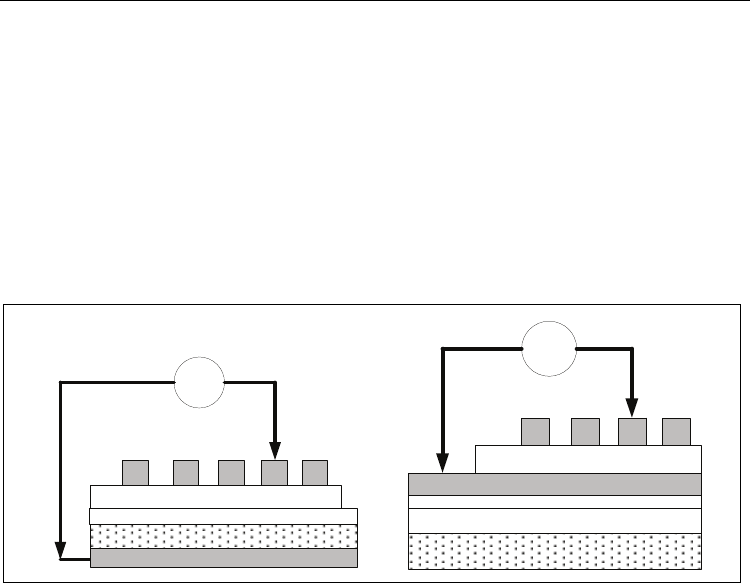
Silicon Substrate
V
Al Al Al Al
Ferroelectric films
Al
Al
SiO
2
films
Silicon Substrate
Pt
V
Al Al Al Al
Ferroelectric films
Ti
SiO
2
films
Fig. 1. (a) Metal-ferroelectric-insulator-semiconductor (MFIS) structure, and (b) Metal
ferroelectric-metal (MFM) structure.
The ferroelectric ceramic target prepared, the raw materials were mixed and fabricated by
solid state reaction method. After mixing and ball-milling, the mixture was dried, grounded,
and calcined for some time. Then, the pressed ferroelectric ceramic target with a diameter of
two inches was sintered in ambient air. The base pressure of the deposited chamber was
brought down 1×10
-7
mTorr prior to deposition. The target was placed away from the
Pt/Ti/SiO
2
/Si and SiO
2
/Si substrate. For metal-ferroelectric-metal (MFM) capacitor
structure, the Pt and the Ti were deposited by dc sputtering using pure argon plasma as
bottom electrodes. The SiO
2
thin films were prepared by dry oxidation technology. The
metal-ferroelectric-insulator-semiconductor (MFIS) and metal-ferroelectric-metal (MFM)
structures were shown in Fig. 1.
For the physical properties of ferroelectric thin films obtained, the thickness and surface
morphology of ferroelectric thin films were observed by field effect scanning electron
microscopy (FeSEM). The crystal structure of ferroelectric thin films were characterized by
an X-ray diffraction (XRD) measurement using a Ni-filtered CuKα radiation. The
capacitance-voltage (C-V) properties were measured as a function of applied voltage by
using a Hewlett-Packard (HP 4284A) impedance gain phase analyzer. The current curves
versus the applied voltage (I-V characteristics) of the ferroelectric thin films were measured
by a Hewlett-Packard (HP 4156) semiconductor parameter analyzer.
Fabrication and Study on One-Transistor-Capacitor Structure of
Nonvolatile Random Access Memory TFT Devices Using Ferroelectric Gated Oxide Film
181
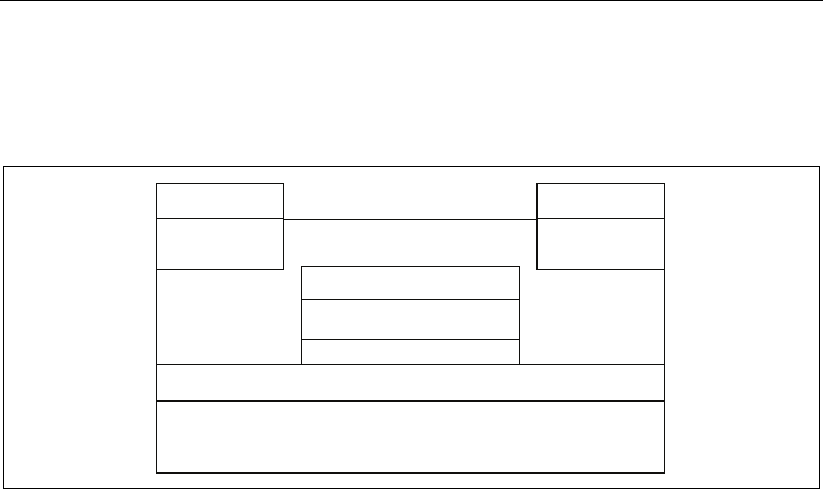
Additionally, the ferroelectric thin films were used in a one-transistor-capacitor (1TC)
structure of the amorphous-Si TFT device to replace the gate oxide of random access
memory devices. For that, a bottom-gate amorphous thin-film transistor, as shown in Fig.2,
would be fabricated and the characteristics of the fabricated devices were successfully
developed.
Silicon Substrate or ITO Substrate
Silicon Dioxide
Ti seed Layer
Pt bottom gate
Al DrainAl Source
n
+
Regionn
+
Region
Amorphous Silicon Layer
Ferroelectric Layer
Fig. 2. The 1TC FeRAM device fabricated with ferroelectric thin film.
For 1TC FeRAM device fabricated, a one-transistor-capacitor (1TC) structure of the
amorphous-Si (a-Si) TFT device was designed and fabricated. In Fig. 2, the a-Si TFT were
fabricated by depositing ferroelectric ferroelectric thin films gate oxide on bottom gate
Pt/Ti/SiO
2
/Si substrate. A silicon oxide film, acting as a buffer oxide, was deposited on
gate oxide substrate by plasma enhanced chemical vapor deposition (PECVD). A
amorphous silicon film, acting as an active channel, was also deposited by PECVD
method. Additionally, the source and drain regions were doped phosphorous by an ion
implantation method. A aluminum films was deposited as the source and drain
electrodes.
Finally, the a-Si TFT was heat treated for 1h in N
2
ambient for the purpose of alloying. The
a-Si TFT with the dimensions of 40 μm in width and 8 μm in length were designed and
fabricated and the I
D
-V
G
transfer characteristics of 1TC FeRAM devices were measured. The
operation characteristic of 1TC structure for TFT devices was similar to SONOS structure of
non-volatile flash memory device.
2.1 ABO
3
and BLSF
s
structure material
The (ABO
3
) pervoskite and bismuth layer structured ferroelectrics (BLSFs) were excellent
candidate materials for ferroelectric random access memories (FeRAMs) such as in smart
cards and portable electric devices utilizing their low electric consumption, nonvolatility,
high speed readout. The ABO
3
structure materials for ferroelectric oxide exhibit high
remnant polarization and low coercive filed. Such as Pb(Zr,Ti)O
3
(PZT), Sr
2
Bi
2
Ta
2
O
9
(SBT),
SrTiO
3
(ST), Ba(Zr,Ti)O
3
(BZ1T9), and (Ba,Sr)TiO
3
(BST) were widely studied and discussed
for large storage capacity FeRAM devices. The (Ba,Sr)TiO
3
and Ba(Ti,Zr)O
3
ferroelectric
materials were also expected to substitute the PZT or SBT memory materials and improve
the environmental pollution because of their low pollution problem [9-15]. In addition, the
Ferroelectrics - Applications
182
high dielectric constant and low leakage current density of zirconium and strontium-doped
BaTiO
3
thin films were applied for the further application in the high density dynamic
random access memory (DRAM) [16-20].
2.1.1 ABO3 pervoskite structure material system
For ABO
3
pervoskite structure such as, BaTiO
3
and BZ1T9, the excellent electrical and
ferroelectric properties were obtained and found. For SOP concept, the ferroelectric BZ1T9
thin film on ITO substrate were investigated and discussed. For crystallization and grain
grow of ferroelectric thin films, the crystal orientation and preferred phase of different
substrates were important factors for ferroelectric thin films of MIM structures. The XRD
patterns of BZ1T9 thin films with 40% oxygen concentration on Pt/Ti/SiO
2
/Si substrates
from our previous study were shown in Fig. 3 [21-22]. The (111) and (011) peaks of the
BZ1T9 thin films on Pt/Ti/SiO
2
/Si substrates were compared with those on ITO substrates.
The strongest and sharpest peak was observed along the Pt(111) crystal plane. This suggests
that the BZ1T9 films grew epitaxially with the Pt(111) bottom electrode. However, the (111)
peaks of BZ1T9 thin films were not observed for (400) and (440) ITO substrates. Therefore,
we determined that the crystallinity and deposition rate of BZ1T9 thin films on ITO
substrates differed from those in these study [21-24].
2θ de
g
ree
20 30 40 50 60
Intensity
ITO (400)
(011)
(001)
ITO (440)
(011)
(001)
(111)
(002)
(112)
Pt (111)
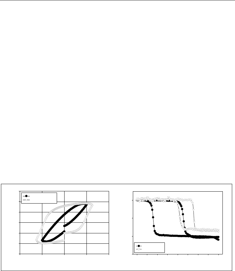
Electrical Field
-1500 -1000 -500 0 500 1000 1500
Polarization
-20
-10
0
10
20
5V
10V
15V
20V
Fig. 3. (a) XRD patterns of as-deposited thin films on the ITO/glass and Pt substrates, and
(b) P-E curves of thin films.
The polarization versus applied electrical field (P-E) curves of as-deposited BZ1T9 thin films
were shown in Fig. 3(a). As the applied voltage increases, the remanent polarization of thin
films increases from 0.5 to 2.5 μC/cm
2
. In addition, the 2P
r
and coercive field calculated and
were about 5 μC/cm
2
and 250 kV/cm, respectively. According to our previous study, the
BZ1T9 thin film deposited at high temperature exhibited high dielectric constant and high
leakage current density because of its polycrystalline structure [21].
2.1.2 Bismuth layer ferroelectric structure material system
Bismuth titanate system based materials were an important role for FeRAMs applications. The
bismuth titanate system were given in a general formula of bismuth layer structure
ferroelectric, (Bi
2
O
2
)
2+
(A
n-1
B
n
O
3n+1
)
2-
(A=Bi, B=Ti). The high leakage current, high dielectric loss
Fabrication and Study on One-Transistor-Capacitor Structure of
Nonvolatile Random Access Memory TFT Devices Using Ferroelectric Gated Oxide Film
183
and domain pinning of bismuth titanate system based materials were caused by defects,
bismuth vacancies and oxygen vacancies. These defects and oxygen vacancies were attributed
from the volatilization of Bi
2
O
3
of bismuth contents at elevated temperature [25-27].
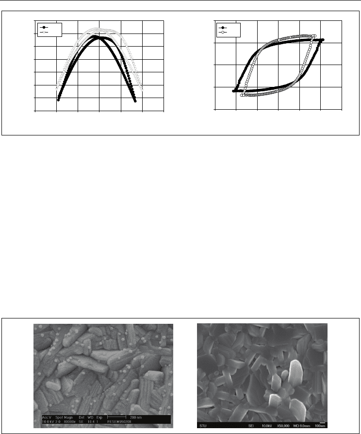
2θ Degree
20 30 40 50 60
Intensity
STD
500
o
C
600
o
C
700
o
C
Pt (111)
(117)
(006)
(008)
(020)
(220)
(317)
Fig. 4. (a) XRD patterns of as-deposited Bi
4
Ti
3
O
12
thin films, and (b)The SEM morphology of
as-deposited Bi
4
Ti
3
O
12
films.
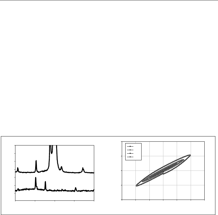
The XRD patterns of as-deposited Bi
4
Ti
3
O
12
thin films and ferroelectric thin films under
500~700
o
C rapid thermal annealing (RTA) process were compared in Fig. 4. From the results
obtained, the (002) and (117) peaks of as-deposited Bi
4
Ti
3
O
12
thin film under the optimal
sputtering parameters were found. The strong intensity of XRD peaks of Bi
4
Ti
3
O
12
thin film
under the 700
o
C RTA post-treatment were be found. They were (008), (006), (020) and (117)
peaks, respectively. Compared the XRD patterns shown in Fig. 4, the crystalline intensity of
(111) plane has no apparent increase as the as-deposited process is used and has apparent
increase as the RTA-treated process was used. And a smaller full width at half maximum
value (FWHM) is revealed in the RTA-treated Bi
4
Ti
3
O
12
thin films under the 700
o
C post-
treatment. This result suggests that crystal structure of Bi
4
Ti
3
O
12
thin films were improved in
RTA-treated process.
The surface morphology observations of as-deposited Bi
4
Ti
3
O
12
thin films under the 700
o
C
RTA processes were shown in Fig. 4. For the as-deposited Bi
4
Ti
3
O
12
thin films, the
morphology reveals a smooth surface and the grain growth were not observed. The grain
size and boundary of Bi
4
Ti
3
O
12
thin films increased while the annealing temperature
increased to 700
o
C. In RTA annealed Bi
4
Ti
3
O
12
thin films, the maximum grain size were
about 200 nm and the average grain size is 100 nm. As shown in Fig. 4, the thickness of
annealed Bi
4
Ti
3
O
12
thin films were calculated and found from the SEM cross-section images.
The thickness of the deposited Bi
4
Ti
3
O
12
thin films is about 800 nm and the deposited rate of
Bi
4
Ti
3
O
12
thin films is about 14 nm/mim.
2.1.3 The influence of doping effect on the electrical properties of ferroelectric films
In the past, we found that using V
2
O
5
as the addition or substitution would improve the
dielectric characteristics of SrBi
2
Ta
2
O
9
ceramics [28]. Vanadium doped Bi
4
Ti
3
O
12
thin films
were also found to have very large remanent polarization (2Pr) and the coercive field (Ec).
Ferroelectrics - Applications
184
But the leakage current density, the memory window and the changing ratio of memory
window of vanadium doped Bi
4
Ti
3
O
12
thin films measured using the MFIS structure were
not developed before [29-31].
Figure 5(a) shows ferroelectric hysteresis loops of Bi
4
Ti
3
O
12
and as-deposited BTV thin film
capacitors measured with a ferroelectric tester (Radiant Technologies RT66A). The as-
deposited BTV thin films clearly show ferroelectricity characteristics. The remanent
polarization and coercive field were 23 μC/cm
2
and 450 kV/cm. To compare the vanadium
doped and undoped Bi
4
Ti
3
O
12
thin films, the remanent polarization (2Pr) were increased
form 16μC/cm
2
for undoped Bi
4
Ti
3
O
12
thin films to 23 μC/cm
2
for vanadium doped.
However, the coercive field of as-deposited BTV thin films would be increased to 450
kV/cm. These results indicated that the substitution of vanadium was effective for the
appearance of ferroelectricity at 550 °C. The 2Pr value and the Ec value were larger than
those reported in Refs. [9-10], and the 2Pr value was smaller and the Ec value was larger
than those reported in [31]. Based on above results, it was found that the simultaneous
substitutions for B-site are effective to derive enough ferroelectricity by accelerating the
domain nucleation and pinning relaxation caused by B-site substitution [32-35].
Figure 5(b) shows the C-V curves of as-deposited vanadium doped BTV and un-doped BIT
thin films. The applied voltages, which are first changed from -20 to 20 V and then returned
to -20 V, are used to measure the capacitance voltage characteristics (C-V) of the MFIS
structures. For the vanadium doped thin films, the memory window of MFIS structure
increased from 5 to 15 V, and the threshold voltage decreased from 7 to 3 V. This result
demonstrated that the lower threshold voltage and decreased oxygen vacancy in undoped
BIT thin films were improved from the C-V curves measured.
Electrical Field (MV/cm)
-1000 -500 0 500 1000
Polarization (μC/cm
2
)
-30
-20
-10
0
10
20
30
undoped
vanadium doped
Applied Voltage(V)
-20 -15 -10 -5 0 5 10 15 20
Normalization Capacitance (nF)
0.4
0.6
0.8
1.0
vanadium doped
undoped
Fig. 5. (a) The P-E characteristics of vanadium doped and undoped thin films, and (b) The
normalization C-V curves of vanadium doped and undoped thin films.
According to pervious study, the Bi
4
Ti
3
O
12
materials exhibit high leakage current and
domain pinning properties because of the defects such as bismuth and oxygen vacancies.
The BTV thin film was prepared by substituting a bismuth ion with a lanthanum ion at A-
site substitution, and the fatigue endurance characteristics was improved [36]. In addition,
the B-site substitution by high-valent cation was mainly the compensation for the defects.
These defects caused by the fatigue phenomenon and strong domain pinning [37-40].
Fabrication and Study on One-Transistor-Capacitor Structure of
Nonvolatile Random Access Memory TFT Devices Using Ferroelectric Gated Oxide Film
185
Applied Voltage (V)
-30 -20 -10 0 10 20 30
Capacitance (nF)
2.10
2.15
2.20
2.25
2.30
2.35
2.40
2.45
BTV
BLTV
Electrical Field (kV/cm)
-600 -400 -200 0 200 400 600
Polarization (
μ
C/cm
2
)
-20
-10
0
10
20
BTV
BLTV
Fig. 6. (a) The C-V characteristics of as-deposited BTV and BLTV thin films, and (b) The P-E
characteristics of as-deposited BTV and BLTV thin films.
Figure 6(a) shows the change in the C-V curves of the BTV and BLTV thin films in MFM
structure measured at 100 kHz. The applied voltages, which were first changed from -20 to
20 V and then returned to -20 V, were used to measure the capacitance voltage
characteristics (C-V). The BLTV thin films exhibited high capacitance than those of BTV thin
films. We found that the capacitances of the lanthanum-doped BTV thin films were
increased.
Figure 6(b) shows the P-E curves of the different ferroelectric thin films under applied
voltage of 18V from the Sawyer−Tower circuits. The remanent polarization of non-doped,
vanadium-doped, and lanthanum-doped ferroelectric thin films linearly was increased from
5, 10 to 11 μC/cm
2
, respectively. The coercive filed of non-doped, vanadium-doped, and
lanthanum-doped ferroelectric thin films were about 300, 300, and 250 kV/cm, respectively.
The ferroelectric properties of lanthanum-doped and vanadium-doped BIT thin films were
improved and found.
Fig. 7. The surface morphology of as-deposited BTV and BLTV thin films.
In Fig. 7, rod-like and circular-board grains were observed with scanning electron
microscopy (SEM) for as-deposited BTV films. The small grain was gold element in
preparation for the SEM sample. However, the BLTV thin films exhibited a great quantity
rod-like grain structure in Fig. 7. The rod-like grain size of BLTV thin films was larger than
those of BTV. We induced that the bismuth vacancies of BTV thin films compensate for
lanthanum addition and micro-structure were improved in BLTV thin films.
Ferroelectrics - Applications
186
2.2 Improved properties for ferroelectric films using post-treatment technology
The electrical and physical characteristics were affected by defect and oxygen vacancy of
grain boundary in various oxide materials for applications in electrical integrated circuits.
The defects and oxygen vacancies in conventional oxide films were usually filled and
compensated by oxygen gas using different deposition methods in the semiconductor
manufacturing process. The crystal structure of the various oxide films was improved by the
high deposition temperature. However, the oxygen elements in grain boundary of the thin
films were broken and lost above the deposition temperatures of 550
o
C [41–47]. To improve
the properties of various oxide materials under the post-treatment process, the conventional
temperature annealing (CTA) and rapid thermal annealing (RTA) processing were
sometimes essential and indispensable technology for crystallization and quality of thin
films [48-52].
2.2.1 CFA and RTA post-treatment technology
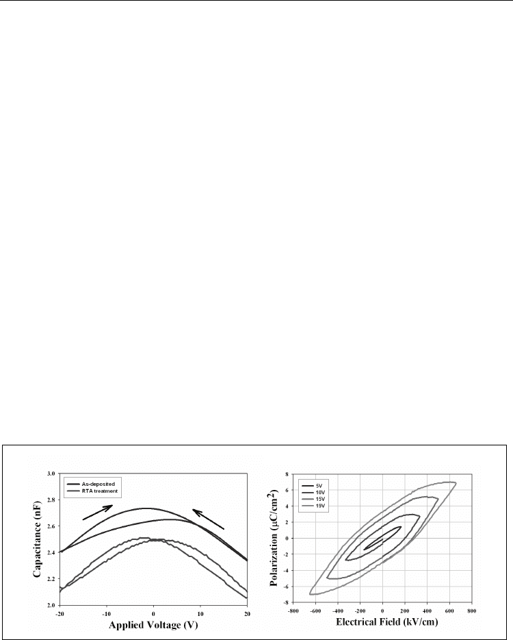
Ferroelectric thin films prepared by rapid temperature annealing (RTA) and conventional
temperature annealing (CFA) processing were reported extensively. Many studies had been
reported that rapid temperature annealing method was successfully to increase the electrical
and physical properties [53-56]. In addition, grain size, electrical properties and surface
roughness are greatly affected by annealing temperature under conventional furnace
annealing.
To study the characteristics of thin films of perovskite oxide BZ1T9, deposited on ITO glass
substrate using the different RTA annealing temperatures were found. In which, the
characteristics of the Al/BZ1T9/ITO glass (MFM) structures, were reported and the
relationship between the electrical properties and different annealing temperature of MFM
structure was investigated. In addition, preferred orientation, crystal phase and dielectric
properties of BZ1T9 thin films by different annealing temperatures were discussion and
evaluated.
Fig. 8. (a) The C-V characteristics of as-deposited and RTA-treated thin films, and (b) The P-
E characteristics of RTA-treated thin films.
Figure 8(a) shows the C-V curves of as-deposited and annealed BZ1T9 films when applied
voltage of ±20V. From the experiments obtained, the capacitance of RTA annealed BZ1T9
films increased while the temperature increased to 650
o
C. Besides, the maximum dielectric

Fabrication and Study on One-Transistor-Capacitor Structure of
Nonvolatile Random Access Memory TFT Devices Using Ferroelectric Gated Oxide Film
187
constant of RTA annealed BZ1T9 films were found. In addition, the larger grain size of
annealed BZ1T9 films were attributed to this reason.
The leakage current density versus applied electrical field (J-E) curves of as-deposited
BZ1T9 films under 650
o
C RTA process were also found. The leakage current densities of as-
deposited BZ1T9 films using RTA process were about 2×10
-6
A/cm
2
under the electrical field
of 0.5 MV/cm. It showed that the leakage current density of annealed-BZ1T9 films was
larger than those of as-deposited BZ1T9.
The P-E curves of as-deposited BZ1T9 thin films at a frequency of 100 kHz was shown in
Fig. 8(b). As the applied voltage increases, the remanent polarization of thin films increases.
In addition, the 2P
r
and coercive field are also calculated and were about 6 μC/cm
2
and 250
kV/cm, respectively. According to our previous study, the BZ1T9 thin film deposited at a
higher temperature exhibits a higher dielectric constant and a higher leakage current density
because of its polycrystalline structure [57].
2.2.2 Oxygen plasma post-treatment technology
The high-temperature process for integrated fabrication on electronic devices was a
serious problem. The gas-like and excellent properties of the oxygen plasma process were
attracted considerable research in efficiently transporting oxygen atom and nodamaging
diffusion into the microstructures of oxide materials at a low-temperature treatment.
Decreased and passivated the traps and defects of oxide materials were the most
advantages.
Figure 9(a) shows the leakage current density versus electrical filed (J-E) curves of as-
deposited BSTZ thin films treated as a function of oxygen plasma treatment times. The
leakage current density of BSTZ thin films was decreased as oxygen plasma treatment times
increased. The leakage current density of treated thin films was lower than those of as-
deposited thin films. We also found that the leakage current density of the BSTZ thin films
for 3 minutes plasma treatment time were similar to those for 6-9 minutes plasma
treatment time. To discuss the defects and oxygen vacancies effect, the leakage current
versus electrical field curves were fitted to the Schottky emission and Poole-Frankel
transport models [58−60]. The fitting curve was straight line, and the J−E curves of as-
deposited thin films after oxygen plasma treatment obey the Schottky emission model in fig.
2. From the experimental results, the low leakage current density of plasma treated thin
films was attributed to less oxygen defects and vacancies.
Figure 8(b) shows the capacitances-voltage (C-V) curves of non-treatment and oxygen
plasma treatment BSTZ thin films. The capacitance of thin films was increased while the
oxygen treatment time increased. The capacitance of thin films was increased. As the results,
the improvement of capacitance of BSTZ thin films were attributed to the oxygen ion
vacancy compensated.
In addition, we found that the wide-scan XPS spectrum of the as-deposited thin film for
oxygen plasma treatment in the binding energy range from 100 to 1keV. From the XPS
spectrum, it revealed that the thin films contained Ba 3d, Sr 3d, Ti 2p, Zr 3d, and O 1s
elements. After oxygen plasma treated, the LBE and HBE were increased to 533.6 and 535.8
eV. These results induced that the oxygen plasma operatively react with the dangling bonds
of thin films and form the stronger O 1s bonding. The O 1s binding energy of the BSTZ thin
film after oxygen plasma treatment was increased.
Ferroelectrics - Applications
188
Electrical Field (MV/cm)
0.00.10.20.30.40.5
Leakage Current Density (A/cm
2
)
10
-10
10
-9
10
-8
10
-7
10
-6
10
-5
10
-4
10
-3
0%
25%
40%
60%
Applied Voltage (V)
-10 -5 0 5 10
Capacitance (pF)
100
150
200
250
300
350
STD
1 min
3 min
6 min
9 min
Fig. 9. (a) The J-E characteristics of as-deposited and plasma-treated BSTZ thin films, and (b)
The C-V characteristics of as-deposited and plasma-treated BSTZ thin films.
For other ferroelectric thin film, the leakage current density versus applied voltage (J-E)
curves of the BZ1T9 thin films was shown in Fig. 5. At an electric field of 0.25 MV/cm, the
oxygen-plasma-treated films exhibit a leakage current density two orders of magnitude
lower than those of the non-oxygen-plasma-treated ones. As mentioned above, the oxygen
plasma treatment decreases the oxygen vacancies and the leakage current density.The
current-field curves were fit to Schottky emission and Poole-Frankel transport models to
determine whether the observed decrease in leakage current of the oxygen plasma treated
films [58-60]. Smyth et al. reported that oxygen escapes during thermal process, and the
oxygen vacancies are subsequently generated according to O
o
<-> V
o
++
+ 2e
-
+ 1/2 O
2
, that
the O
o
, V
o
++
, and e
-
denote the oxygen ion at its normal site, oxygen vacancy, and electron,
respectively. For that, a lot of oxygen vacancies will exist after 9 min the oxygen plasma
treatment.
Electrical Field (MV/cm)
-0.25 0.00 0.25
Polarization (μC/cm
2
)
-20
-10
0
10
20
No plasma treated
Oxygen plasma treated
Electrical Field
(
MV/cm
)
0.00 0.05 0.10 0.15 0.20 0.25 0.30
Leakage Current Density (A/cm
2
)
10
-8
10
-7
10
-6
10
-5
No plasma treated
6 min plasma treated
9 min plasma treated
Fig. 10. (a) The P-E characteristics of as-deposited and plasma-treated BZ1T9 thin films, and
(b) The J-E characteristics of as-deposited and plasma-treated BZ1T9 thin films.
Figure 10(a) shows the P-E curves of the BZ1T9 films observed at a frequency of 100 kHz
under an applied electrical field of 0–0.28 MV/cm from the Sawyer-Tower circuits. After
oxygen plasma treatment, the coercive field does not appear to change; however, the
remnant polarization appears to increase from 6 to 9 μC/cm2. As shown in Fig. 10(b), we