Leroy C., Rancoita P.-G. Principles Of Radiation Interaction In Matter And Detection
Подождите немного. Документ загружается.

January 9, 2009 10:21 World Scientific Book - 9.75in x 6.5in ws-bo ok975x65˙n˙2nd˙Ed
760 Principles of Radiation Interaction in Matter and Detection
As stressed above, the detector can be operated selecting, at the same time,
photoelectric and Compton photon interactions. In this way, up to 43% of the
impinging photons provide events for the image formation. However, in order to
reduce the background of low and medium energy photons, generated by Compton
interaction in the patient’s body, a metallic Sn filter can be utilized. It reduces to
a negligible amount the γ’s with energy lower than 100 keV.
The detector can also be operated by selecting photoelectric interacting photons
alone, which are about 4% of the total number of 140.5 keV incoming photons. It
achieves a very high energy resolution of about 1%. In this way, a strong reduction
of background, due to photons interacting in the patient’s body, is expected. Thus,
highly resolved images are expected, even if the number of counted events is reduced.
The photoelectric operational mode seems very attractive for extending the
usage of SiCPICal to lower energy photons, for which the photoelectric cross sec-
tion increases. In the (60–80) keV photon energy range, the photoelectric interaction
probability in SiCPICal is (43–23)%, and the energy resolution is (2.3–1.7)%.
The possibility of using high-Z semiconductor materials like cadmium telluride
(CdTe and CdZnTe) and mercuric iodide (HgI
2
) has been envisaged. These ma-
terials, widely available, present however drawbacks for their use in SPECT de-
tectors. Indeed, hole transport is poor in these materials and charges are heavily
trapped and cannot be collected in a practical amount of time. Due to incomplete
charge collection, the size of the output pulse becomes dependent on the exact po-
sition of interaction of the radiation in the detector volume, and spoils the energy
resolution. The accumulation of uncombined trapped charges leads to polarization,
which further inhibits the charge collection. Overall, the performances of the de-
tector can change over a period of time. However, it is possible to build CdZnTe
imaging devices that only relies on the collection of electrons. A device of this type
(the coplanar orthogonal anode detector) has been successfully tested [Tousignant
et al. (1999)] and is able to measure the position of interaction in 3-dimensions with
a spatial resolution of 300 µm and an energy resolution of 1% and 2.6% FW HM
at 662 keV and 122 keV, respectively. Bridgman CdTe and CdZnTe crystal growth,
with cadmium vapor pressure control, can produce crystals that are highly donor
doped and highly electrically conducting. After annealing in tellurium vapors, they
are transformed into highly compensated state of high resistivity and high sensi-
tivity to photons [Lachish (1999)]. These detectors, after proper equipment with
ohmic contacts and a grounded guard-ring around the positive contact, have fast
electron collection time: for a detector d = 1 mm thick operated at a bias of 150 volts
(electron and hole mobility, µ
e
≈ 1000 cm
2
V
−1
s
−1
, and µ
h
≈ 70 cm
2
V
−1
s
−1
, respec-
tively), the transit time of an electron from contact to contact is
t = d
2
/(µ
e
V ) = 66 ns , (11.4)
while the transit time for a hole (should there be no trapping) under the same
conditions is:
t ≈ 1 µs. (11.5)
January 9, 2009 10:21 World Scientific Book - 9.75in x 6.5in ws-bo ok975x65˙n˙2nd˙Ed
Medical Physics Applications 761
Adjusting the shaping time of the charge collection system [(50–120) ns], such a
detector is not sensitive to hole trapping and only collects the electron contribution
to the signal.
The Compton camera concept is emerging for SPECT applications. However,to
our knowledge, no practical application has been achieved yet. The real prospect
in that direction is represented by the Medipix detector device (Sect. 6.5.1). The
Compton camera is based on a method which allows the reconstruction of the direc-
tion of the primary photon coming from the object to be imaged by iterative back
projection methods [Brechner and Singh (1990)]. Therefore, a Compton camera can
be operated without collimator, offering a great advantage over Anger camera. This
absence of collimator translates into higher detection efficiency. The Compton ca-
mera should permit the acquisition of data representing multiple angular views of
the source distribution from a single position consequently reducing the need of ca-
mera motion. This increased sensitivity allows also a reduction of the dose delivered
to the patient (lower activity level and shorter half-lives) and a reduction of the
time spent by the patient in front of the scanner (complete immobility of the pa-
tient which could be painful just after surgery or during a suffering period). Reduced
angular motion of the camera, meaning less time spent between angular stops, also
help this latter aspect. The absence of a collimator has another important implica-
tion as this piece of metal is heavy and its insertion in the detecting system could
alter the precision and mechanical stability of the system.
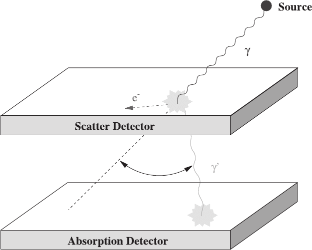
In principle, the Compton camera consists of a scatter detector and a absorption
detector (Fig. 11.2).
The scatter detector generates and detects Compton interactions. The Comp-
ton scattered photons are depositing their energy in the absorption detector. The
material of the scattering detector must have sizable Compton scattering cross-
sections for the energy of photon released by the source (standard energy range
from 100 up to 600 keV). Semiconductors, such as Si and GaAs of large thicknesses
(1 mm and more), are usually envisaged for active medium of the scatter plane. The
material composing the absorption detector should have large photo-absorption
cross-sections in this energy range. Usually NaI(Tl), CsI(Tl) and BGO are used for
absorption detector. The use of heavy semiconductors such as CdZnTe (CZT) is
also possible.
The energy of the photons emitted by the source is known exactly. Therefore,
the sum of energies deposited in the scattering and absorption detectors can be used
to reject photons produced by Compton scattering in the patient.
The photon energy after Compton scattering in the scatter plane, E
A
, is related
to the incident photon energy, E
0
, via Eq. (11.1). E
A
is also the energy deposited
in the absorption detector. E
S
is the energy lost by the photon in the scatter plane
and this energy is converted into kinetic energy of the recoil electron. Applying the
conservation of energy, one finds
E
S
= E
0
− E
A
. (11.6)
January 9, 2009 10:21 World Scientific Book - 9.75in x 6.5in ws-bo ok975x65˙n˙2nd˙Ed
762 Principles of Radiation Interaction in Matter and Detection
Fig. 11.2 The Compton camera with a scatter plane and an absorption plane. The location of
photon impact in the scatter plane is obtained from the measurement of the recoiling electron. The
Compton scattered photon is absorbed in the absorption plane.
The locations of the two interactions (one in the scattering detector and the
second in the absorption detector), coupled with the scattering angle, limits the
photon possible source location to a cone whose axis is in line with the positions of
the two interactions and an aperture defined by the scattering angle. The reconstruc-
tion of the source distribution is going through the reconstruction of the direction
of the primary photon coming from the object to be imaged. This reconstruction
is performed by iterative back projection methods (see for instance [Brechner and
Singh (1990)]).
As an illustration of the scatter plane role in a Compton camera principle, let
us calculate the number of Compton events generated in a scatter plane made of
silicon by a gamma emitting source that is injected into a patient. The source is
99m
Tc with a typical dose injection of 2 µCi.
99m
Tc emits photons of 140.5 keV
energy. The probability of having a photon of a specific energy emitted in a decay
is represented by the factor p. For the example of
99m
Tc, p = 0.889 for a photon
energy of 140.5 keV.
The activity of the radioisotope is measured in transformation per second. The
special unit of activity is the becquerel (Bq, 1 Bq = 1 transformation/sec) that is

January 9, 2009 10:21 World Scientific Book - 9.75in x 6.5in ws-bo ok975x65˙n˙2nd˙Ed
Medical Physics Applications 763
expressed in curies (Ci)
1 Ci = 3.7 × 10
10
Bq. (11.7)
The numb er of atoms, N
A
, present in the source and the activity, A, of the source
are related by the transformation constant λ as:
A = λN
A
, (11.8)
where
λ =
ln 2
t
1/2
=
0.693
t
1/2
and t
1/2
is the half-life of the radioisotope. One should note that the mean-life of
the radioisotope is
τ =
1
λ
= 1.443 × t
1/2
.
The activity decays with time, t, according to an exponential law, as:
A = λN
A
= λN
0
e
−λt
= A
0
e
−0.693t/t
1/2
. (11.9)
In the equation above, A
0
= λN
0
with N
0
is the number of atoms present at t = 0.
The source inside the body is eliminated by natural means. Some radiophar-
maceuticals are being eliminated faster, some slower but it usually takes a few
hours. The effective half-life, t
1/2
(eff), is calculated by adding physics λ and biolo-
gical λ
bio
, i.e.,
λ(eff) =
ln 2
t
1/2
(eff)
= λ + λ
bio
.
The half-life of
99m
Tc is t
1/2
= 6.02 hours and τ = 8.69 hours. The total number
of photons, N
ph
, of energy 140.5 keV emitted by the
99m
Tc source during a perio d
of time t is:
N
ph
= p N
0
³
1 − e
−0.693t/t
1/2
´
. (11.10)
Therefore, the number of 140.5 keV photons emitted by the source after one hour
(N
0
= 7.4 × 10
4
for a
99m
Tc injection dose of 2 µCi which corresponds to 7.4 × 10
4
transformations/sec) is
N
ph
∼ 0.7 × 10
4
. (11.11)
Assuming no attenuation between the source and the detector and an isotropic emis-
sion of the source, the number of 140.5 keV incident photons reaching the detector
can be defined as:
N
incident
= fN
ph
with
f =
area of the detector
4π (distance to the source)
2
. (11.12)

January 9, 2009 10:21 World Scientific Book - 9.75in x 6.5in ws-bo ok975x65˙n˙2nd˙Ed
764 Principles of Radiation Interaction in Matter and Detection
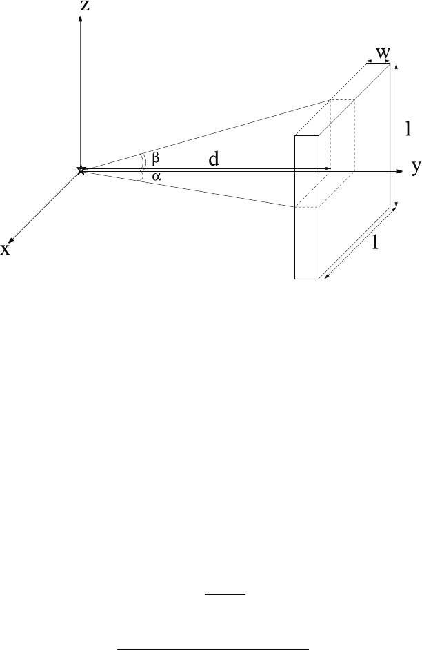
We consider a scatter plane made of pads or pixels of silicon detectors representing a
total area of 1.4 cm ×1.4 cm (such as a MediPix device, Sect. 6.5.1) and a thickness
of 1 mm, typical for medical applications (Fig. 11.3). Then, the fraction f of photons
reaching the sensitive layer, located at 1 cm from the source, is [using Eq. (11.12)]
f ∼ 0.2,
giving the number of photons reaching the sensitive layer:
N
incident
∼ 1400. (11.13)
The number of photons, N
int
, interacting in the detector of thickness ∆y is given
by:
N
int
= µN
incident
∆y, (11.14)
where µ is the total attenuation coefficient. It is the sum of four components (see
Sect. 2.3.5): the photoelectric (τ
pe
), the coherent scattering (σ
coh
), the Compton or
incoherent scattering (σ
C
) and the pair production (κ
pair
) attenuation coefficients,
i.e.,
µ = τ
pe
+ σ
coh
+ σ
C
+ κ
pair
.
Equation 11.14 is an approximation which is valid because the detector width is
small. A more precise calculation would use
N
int
= fN
ph
¡
1 − e
−µ∆y
¢
. (11.15)
The percentage of the Compton interactions is:
100σ
C
/(τ
pe
+ σ
coh
+ σ
C
+ κ
pair
).
The number, N
C
, of Compton scattered photons in the detector of thickness ∆y in
the scatter plane is:
N
C
= N
int
× σ
C
/µ = µ N
incident
∆y σ
C
/µ, (11.16)
using Eq. (11.14). For a
99m
Tc source, at the photon energy of 140.5 keV, we have
σ
C
ρ
= 1.33 × 10
−1
cm
2
/g.
The silicon density being 2.33 g/cm
3
, one has a linear Compton scattering attenua-
tion coefficient σ
C
= 0.30989 cm
−1
. Then, the average number of Compton scat-
tered photons in the scatter plane per second for one hour of source decay for a dis-
tance detector-source of 1 cm and an injected dose of 2 µCi [using Eqs. (11.13, 11.16)
with ∆y = 0.1 cm]:
N
C
∼ 44 s
−1
.
The previous calculation was obviously approximate. If the distance between the
detector and the source is not so small compared with the detector’s dimensions,
one should use an exact formula to calculate f∆y:
f∆y = 4 ×
Z
l/2
0
dx
Z
l/2
0
dz
∆y
4π(x
2
+ z
2
+ d
2
)
.

January 9, 2009 10:21 World Scientific Book - 9.75in x 6.5in ws-bo ok975x65˙n˙2nd˙Ed
Medical Physics Applications 765
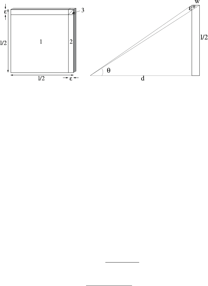
Because of the finite size of the detector, the area l/2 × l/2 has to be divided (as
indicated in Fig. 11.4) in order to calculate ∆y correctly:
² =
wl
2(d + w)
.
In region 1, we have
∆y = w
p
1 + tg
2
α + tg
2
β =
w
d
p
x
2
+ z
2
+ d
2
.
In regions 2 and 3, we obtain
∆y =
µ
l
2
− x
s
1 +
1
tg
2
α
+
tg
2
β
tg
2
α
=
µ
l
2x
− 1
p
x
2
+ z
2
+ d
2
.
We now find:
f∆y = 4 ×
Z
l/2−²
0
dx
Z
l/2−²
0
dz
w
d
√
x
2
+ z
2
+ d
2
4π(x
2
+ z
2
+ d
2
)
+ 8 ×
Z
l/2
l/2−²
dx
Z
l/2−²
0
dz
µ
l
2x
− 1
w
d
√
x
2
+ z
2
+ d
2
4π(x
2
+ z
2
+ d
2
)
+ 8 ×
Z
l/2
l/2−²
dx
Z
x
l/2−²
dz
µ
l
2x
− 1
w
d
√
x
2
+ z
2
+ d
2
4π(x
2
+ z
2
+ d
2
)
.
Finally, we obtain
f∆y =
w
πd
Z
l/2−²
0
dx
Z
l/2−²
0
dz
1
√
x
2
+ z
2
+ d
2
+
2
π
Z
l/2
l/2−²
dx
Z
l/2−²
0
dz
µ
l
2x
− 1
1
√
x
2
+ z
2
+ d
2
+
2
π
Z
l/2
l/2−²
dx
Z
x
l/2−²
dz
µ
l
2x
− 1
1
√
x
2
+ z
2
+ d
2
.
This last integral can only be evaluated numerically.
From Eq. (11.17), it is easy to see that the minimum energy of the scattered
photon will be: E
A
= 90.7 keV, where
E
A
=
E
0
1 + E
0
(1 − cos θ)/mc
2
, (11.17)
where θ is the scattering angle, E
0
= 140.5 keV and m c
2
= 0.511 keV is the electron
rest mass. The average energy of the scattered photon is E
A
≈ 114 keV. This was
taken from the graph found in [Johns and Cunningham (1983)] representing the
fraction of the photon’s energy transferred to the electron as a function of the
energy of the incident photon.
The energy of the electron recoil is about 26 keV. The signal in the scatter silicon
detector is in electron equivalent:
26 keV/3.62 eV = 7, 200 e
−
, (11.18)
January 9, 2009 10:21 World Scientific Book - 9.75in x 6.5in ws-bo ok975x65˙n˙2nd˙Ed
766 Principles of Radiation Interaction in Matter and Detection
Fig. 11.3 Idealized representation of a source-detector system.
which corresp ond to a collected charge of 7, 200 × 1.610
−19
C ≈ 1.2 fC. There are
two sources of noise: the noise from the preamplifier and the noise from leakage
current. Typical preamplifier noise for a shaping time of 2 µs is
ENC[preamp] = 60e
−
+
¡
11e
−
/pF
¢
C
det
.
The silicon detector used for the estimate has a capacitance of
C
det
= 1.05pF/cm × 2.0 cm
2
/0.1 cm ≈ 21 pF
and therefore ENC[preamp] = 290e
−
. The leakage current of silicon detectors
strongly depends on temperature [see Eq. (6.77)] and contributes to a large ex-
tent to the detector noise, spoiling energy and spatial resolution. Therefore, it is
needed to operated silicon detectors at temperature as low as possible (low means,
in practical cases, room temperature and lower). However, standard planar (float-
zone) silicon detector can be safely operated at ro om temperature with a leakage
current at the level of a few nA/cm
2
. Typical noise from leakage current for a shap-
ing time of 2 µs is ENC[leakage] = 150
p
I
r
(nA). For a detector of the type and size
used in the calculation, I
r
≈ 2 nA giving ENC[leakage] = 212 e
−
. The total noise is
then
ENC =
q
ENC[preamp]
2
+ ENC[leakage]
2
≈ 360 e
−
and a signal to noise ratio
S/N ∼ 20.
First feasibility experimental studies of using silicon pad detectors as scatter
plane of a Compton camera has been reported in [Weilhammer et al. (1995)]. These
January 9, 2009 10:21 World Scientific Book - 9.75in x 6.5in ws-bo ok975x65˙n˙2nd˙Ed
Medical Physics Applications 767
pads were consisting of ∼ 345µm thick detectors with size as low as 150 µm ×150 µm
covering an area of 2.4 mm segmented electrodes on one side which were connected to
their individual signal processing circuits through metal lines on top of the detector.
Fig. 11.4 Illustration of the divisions necessary to calculate ∆y precisely.
The next step is to shrink the size of the silicon pads, down to the micrometer
scale, and to finally achieve the stage of pixel detectors, each pixel detector being on
very small electrode. Each detecting units is composed of one single diode attached
to its own readout electronics, the diode being finely segmented, providing high
two-dimensional spatial resolution. The concept of active pixel detectors rely on
electronics cells being equally dimensioned and close to the corresponding pixel,
keeping the collection electrode capacitance very small and a large signal-to-noise
ratio. The application of the concept of silicon (and other type of semiconductors)
pixel arrays to practical systems for medical imaging is under way [Mikulec (2000)].
As discussed in Sect. 6.3.1, semiconductor detectors may achieve very good
energy resolution (σ
R
) because a large number of electron-holes is created inside the
semiconductor. However, other contributions can limit the overall energy resolution,
for instance those depending on the particular readout electronic chain used for the
measurements.
The dependence of angular uncertainties on the energy resolution has to be taken
into account. Several models to calculate these angular uncertainties exist and differ,
according to the way the energy discrimination is done [Ordonez, Bolozdynya and
Chang (1997a)]. If the energy discrimination is done with the scatter detector, E
S
is
measured in the scatter detector. Combining Eqs. (11.1, 11.6), the scattering angle
is:
cos θ = 1 + mc
2
E
S
E
0
(E
S
− E
0
)
. (11.19)
The angular uncertainties are:
σ
θ
=
mc
2
σ
E
S
(E
0
− hE
S
i)
2
sin θ
, (11.20)

January 9, 2009 10:21 World Scientific Book - 9.75in x 6.5in ws-bo ok975x65˙n˙2nd˙Ed
768 Principles of Radiation Interaction in Matter and Detection
Table 11.2 Positron emitting isotopes currently used in PET.
e
+
emitting half life production e
+
effective range end point
isotope (minutes) reaction in body (mm) energy (MeV)
18
F 110.
18
O(p,n)
18
F 1.4 0.635
15
O 2.
15
N(p,n)
15
O,
14
N(d,n)
15
O 4.5 1.7
13
N 10.
16
O(p,α)
13
N 3.0 1.20
11
C 20.
14
N(p,α)
11
C 2.1 0.97
where hE
S
i is the mean value of the E
S
measurements; σ
E
S
has the standard form
σ
E
S
= k
p
a + bE
S
,
where k, a and b depend on the material used for the scatter detector.
If the energy discrimination is done, instead, with the absorption detector, E
A
is measured in the absorption detector. Equation (11.19) can be rewritten as
cos θ = 1 + mc
2
(E
A
− E
0
)
E
0
E
A
. (11.21)
The angular uncertainties are:
σ
θ
=
mc
2
σ
E
A
hE
A
i
2
sin θ
, (11.22)
where hE
A
i is the mean value of the E
A
measurements; σ
E
A
can also be parame-
terized as
σ
E
A
= k
0
p
a
0
+ b
0
E
A
,
where k
0
, a
0
and b
0
depend on the material used for the absorption detector.
There exist other ways to discriminate energy. The scattering angle can be cal-
culated with both measured energies E
S
and E
A
:
cos θ = 1 − mc
2
E
S
E
0
E
A
. (11.23)
The resulting angular uncertainties are:
σ
θ
=
mc
2
E
0
hE
A
i
2
sin θ
p
(hE
A
i σ
E
S
)
2
+ (hE
S
i σ
E
A
)
2
. (11.24)
If one takes into account that the photon emitted by the source can interact with
moving electrons bound to nuclei, one has to use the concept of electron pre-collision
momentum [Ordonez, Bolozdynya and Chang (1997b)]. One defines
p
z
= −mc
E
0
− E
A
− E
0
E
A
(1 − cos θ) /mc
2
p
E
2
0
+ E
2
A
− 2E
0
E
A
cos θ
. (11.25)
Here p
z
is the projection of the electron’s pre-collision momentum on the momen-
tum transfer vector of the photon. The effects of electron motion on the angular
uncertainty are described by [Ordonez, Bolozdynya and Chang (1997b)]
σ
θ
=
1
A
θ
2
£
(A
S
σ
E
S
)
2
+ (A
A
σ
E
A
)
2
+ (A
p
z
σ
p
z
)
2
¤
, (11.26)

January 9, 2009 10:21 World Scientific Book - 9.75in x 6.5in ws-bo ok975x65˙n˙2nd˙Ed
Medical Physics Applications 769
where
A
θ
=
µ
1
mc
2
−
hp
z
i
mcw
hE
A
iE
0
sin θ, (11.27)
A
S
= 1 −
hE
A
i
mc
2
(1 − cos θ) +
hp
z
i
mcw
(E
0
− hE
A
icos θ) , (11.28)
A
A
=
µ
1
mc
2
−
hp
z
i
mcw
(hE
A
i + E
0
) (1 − cos θ) , (11.29)
A
p
z
=
w
mc
, (11.30)
with
w =
q
E
2
0
+ hE
A
i
2
− 2E
0
hE
A
icos θ. (11.31)
Here hE
S
i, hE
A
i, and hp
z
i represent the mean value of E
S
, E
A
, and p
z
, respecti-
vely. The parameter σ
p
z
, appearing in the Doppler broadening term (A
p
z
σ
p
z
), can
be estimated from the width of the total Compton profile, J
n
(p
z
), of the target
nucleus [Biggs, Mendelsohn and Mann (1975)].
Heavier semiconductors, i.e., semiconductors with larger atomic numb er such as
GaAs or CdZnTe, can be used as absorption plane of Compton camera. For heavier
semiconductors, the photoelectric effect has the same magnitude or dominates over
Compton scattering and represents the largest contribution to the total attenua-
tion of photons in the material. In the case of GaAs, for 140.5 keV photons, the
photoelectric absorption is 0.0139 cm
2
/g compared to the Compton scattering con-
tribution of 0.0115 cm
2
/g. For CdZnTe, the photoelectric absorption is 0.0108 cm
2
/g
and the Compton scattering contribution is 0.0457 cm
2
/g.
11.2 Positron Emission Tomography (PET)
Positron emission tomography (PET) is a nuclear medical imaging technique, which
relies on the measurement of the distribution of a radioactive tracer or radiophar-
maceutical labeled with a p ositron emitting isotope injected into a patient.
Several positron emitters are used for the purpose of PET. The most com-
mon emitters are
11
C,
13
N,
15
O and
18
F. The radiopharmaceutical, labeled with a
positron emitting isotope, is a form of glucose which is injected into the patient. The
PET scan will reveal areas where the glucose is consumed in excess of the normal
bo dy needs, such as in a growing tumor.
The emitter lifetime is obviously very important, since it must be large enough
to allow the transportation of practical doses from the production facility to the
location, where the patient is treated. At the same time, the radioisotope has to
be short lived enough to reduce the amount of activation left into the patient. The
half-life of several emitters are listed in Table 11.2.
The radioactive tracer 2-[
18
F]fluro-2-deoxy-D-glucose (
18
FDG) is a substance
widely used in nuclear medicine for nuclear imaging. The radioactive element is the