Melitz W., Shena J., Kummela A.C., Lee S. Kelvin probe force microscopy and its application
Подождите немного. Документ загружается.

W. Melitz et al. / Surface Science Reports 66 (2011) 1–27 11
The chemical state of tip and tip–sample distance can affect
the measured LCPD on a semiconductor surface. Fig. 12 shows
LCPD contrast changes due to the different tip condition caused
by gentle tip crashing onto the sample surface. LCPD contrast is
not observed initially between the row and trough on InAs(001)-
(4
× 2) surface (note that the experimental results in Fig. 12 were
performed by the authors). After gentle crashing of the tip onto
the surface (position 1), LCPD contrast can be observed between
row and trough. The sudden jump in the frequency shift (df) vs. z
spectroscopy curve (curve 1) may imply that the tip crashes into
the sample surface. The tip crashing may rearrange the atoms on
the apex of tip, which may change the chemical state of tip-end
and the tip–sample distance. At position 2, the tip crashes again,
and the LCPD contrast increased significantly. However, at position
3, the contrast spontaneously reverses, caused by the alteration
of the apex structure by the interaction with the surface. df
(z)
spectra are taken at points 2 and 3 [curves 2 and 3 in Fig. 12(c)] and
showed different force–distance dependence, which imply that the
tip states are changed.
In summary, the LCPD contrast is an effect of a bias dependent
short-range interaction force between the tip apex atom and the
underlying surface. The mechanism of this interaction force will
be highly dependent of the system of interest. For a Si tip imag-
ing a semiconductor surface, the short-range interaction is likely to
be caused by covalent interactions similar to atomically-resolved
non-contact AFM [7]. Similarly, the ionic interactions between the
tip and the surface produce the ionic solid short-range force. The
measured LCPD is not a true representation of any one electro-
static, covalent, or ionic interaction. The LCPD is a function of the
bias dependent short-range forces that apply to the particular sam-
ple type. Currently, no sub-nanometer resolution LCPD has been
reported for a non-polar surface such as a metal surface. Further
studies will make it clear which short-range force dominates the
LCPD contrast for particular systems. The LCPD is also a combi-
nation of both the microscopic and mesoscopic interactions. The
combination of these interactions causes an over-estimation of the
true surface potential distribution, making physical interpretations
of experimental results of LCPD measurements difficult. Recently,
Sadewasser et al. suggested the LCPD variation on a semiconductor
surface is caused by the formation of a local surface dipole, due to
the charge transfer between different surface atoms or the charge
redistribution by the interaction with AFM tip [42]. Models includ-
ing accurate tip geometries and tip–sample separations are needed
for the extraction of physical values from the measured LCPD. The-
oretical calculations for both ionic solids and semiconductors show
the tip geometry effects on the measured LCPD. Further theoretical
analysis is needed to develop modeling tools to extract meaningful
results from the measured LCPD. Nevertheless, the LCPD can give
insight to the surface electronic properties.
3. Application of high-resolution KPFM
The following section reviews the application of high-resolution
KPFM to characterize the electrical properties of metallic nanos-
tructures and semiconductor surfaces and devices. Since the work
function or surface potential strongly affect the chemical and phys-
ical phenomena taking place at the surface, KPFM reveals critical
information on the physical and chemical changes of the surface
condition, needed for understanding physical and chemical phe-
nomena on metal/semiconductor surfaces and devices.
3.1. Electrical properties of metallic nanostructures
In recent years, metallic nanostructures have been used in new
devices such as high-efficient heterogeneous catalysts [43–45]
and high-sensitivity chemical/biological sensors [46]. For these
applications, charge transfer between metal nanostructures and
substrates (in heterogeneous catalysts), and between metal nanos-
tructures and chemical/biological molecules interfaces (in chem-
ical/biological sensors) are critical to describe and understand.
The charge transfer inherently modulates potentials on the metal
nanostructure. Therefore, KPFM provides insight into the physics
of metal-nanostructure device applications.
3.1.1. KPFM on metallic nanostructures
Gold is a model material to study the formation of metallic
nanostructures, due to the stable chemical properties and large
atomic size. Goryl et al. showed the work function of deposited
Au nanostructures was independent of the size of the Au
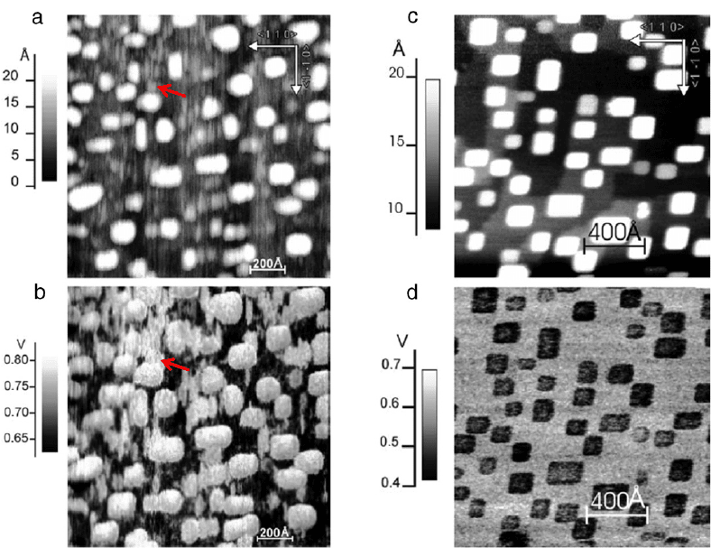
nanostructure [23,47]. Fig. 13(a) and (b) show the topography
and corresponding work function mapping of Au nanostructures
grown on InSb(001) surface at 400 K. Au grows predominantly in
rectangular island shapes. The typical height of a Au nanostructure
is a few monolayers (MLs) (about 2.0 nm).
The work function mapping provides more details about
surface topography. The small features, difficult to observe in the
topography image due to a large variation in topography, are
distinguishable with the help of the work function signal. The small
features between Au nanostructures are indicated by arrows in
Fig. 13(a) and (b). The work function of small features is the same
as the Au nanostructures, which implies the chemical composition
of the small features is similar to the Au nanostructure. KPFM
is able to give information about the chemical composition of
nano-scale features. Graham reported the measured work function
on a Au/W(001) system saturates at a coverage of 3 MLs Au,
which is close to the work function value of bulk Au [48].
Adsorbate–substrate reactions can also be observed. The contrast
between the Au nanostructures and InSb substrate is reversed after
high temperature annealing, because a Au nanostructure has lower
work function than the substrate after post-deposition annealing
(PDA) at 650 K for 2 h. This suggests a Au nanostructure might react
with the InSb substrate and form alloys with In atoms, resulting in
a decreasing working function of the nanostructure. Note that the
surface potential of the InSb substrate did not change after PDA.
Depending on the substrate and surface defects, metallic
nanostructures can form different structures. Recent KPFM results
show surface potential differences between terrace and step edges
on UHV-cleaved semiconductors, alkali halides, and insulating
materials, attributed to charged defects [18,49,50]. Charged defects
are considered to be nucleation sites for metallic nanostructure
growth [51,52]. Barth et al. have investigated Au nanostructures
on alkali halide (001) surfaces using KPFM to study whether metal
nanostructures will screen defect charges or become charged [53],
an important factor for catalytic processes. The charge transfer
will significantly affect the surface and nanostructure properties.
Finally, charge transfer will change states governing the catalytic
reactivity of adsorbates [54].
Fig. 14(a) and (b) show the topography and surface potential
images of a UHV-cleaved KCl surface. The bright features on
potential image show 0.7 eV larger work function than the rest
of the surface terrace sites, attributed to the charged defects. For
0.04 MLs, Fig. 14
(c) and (d), and 1.44 MLs, Fig. 14(e) and (f), of
Au deposition at 200
°C, Au nanostructures are homogeneously
distributed over the terraces with an increased density at step
edges, which causes one-dimensional nanostructure growth.
KPFM results show that some of Au nanostructures have higher
work functions than other Au nanostructures, although they
look very similar in topography images. One explanation is the
nanostructures with higher work function exist above the charged
surface defects. After Au deposition, charge transfer may occur
between surface defects and Au nanostructures deposited on the
defects. The charge transfer from defects to Au nanostructures
increases the work function.
12 W. Melitz et al. / Surface Science Reports 66 (2011) 1–27
Fig. 13. The topography and work function profiles of Au nanostructures on InSb(001) surface with and without post-deposition annealing (PDA). (a) FM mode KPFM
topography and (b) corresponding work function mapping of 0.2 MLs Au grown on InSb(001) surface at 400 K. (c) FM mode KPFM topography and (d) corresponding work
function mapping of Au deposited on InSb surface at 300 K with PDA at 650 K for 2 h. The small features between Au nanostructures are highlighted by arrows in Fig. 13(a)
and (b).
Source: Adapted from [47].
3.1.2. Charge transfer in metallic nanostructure catalyst
Metallic nanostructures supported on thin oxide films such
as TiO
2
or MgO are known to exhibit extraordinary catalytic
properties in oxidation reactions [43,51,55–57]. In catalytic
reactions, charge transfer between metallic nanostructures and
supported oxide films is important to investigate, since the charge
transfer from a metal nanostructure to the supporting substrate
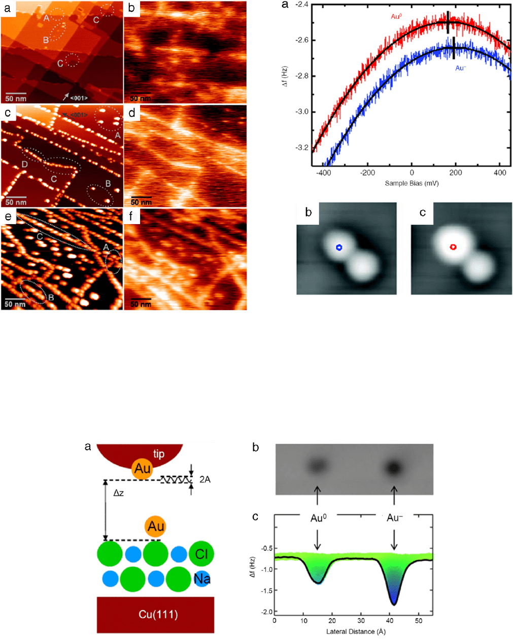
can affect catalytic reactions on the metal surface. Recently, Gross
et al. used a q-Plus non-contact AFM/KPFM system to probe single
atoms on the surface [58]. They show KPFM not only allows single
atoms to be imaged, but also can be used to detect the charge state
of a single atom on thin insulating films.
For the model system, single Au atoms on bilayer ultrathin NaCl
films on Cu(111) are used as shown in Fig. 15(a). In constant height
imaging mode, frequency shift signals were recorded, Fig. 15(b).
Charging of a gold adatom by one electron charge increased the
force on the AFM tip by a few pico-newtons, indicating a higher
attractive force above a negatively charged Au atom
(Au
−
) than
above a neutral Au atom (Au
0
). Density function theory reveals
that the large ionic polarizability of the NaCl film is responsible for
the stability of the two different charge states [59]. An additional
electron on the gold atom forces the Cl
−
ion underneath a Au
atom to move downward, whereas the surrounding Na
+
ions move
upward. This relaxation pattern creates an attractive potential for
the additional charge on the Au atom, which is consistent with
increase in the absolute value of frequency shift. This work showed
a very high sensitivity for detecting the single electron charge.
The high sensitivity was achieved by using very small oscillation
amplitude (typically 40 pm) and low temperature (5 K) imaging.
Note that the experiment was done by a tuning folk system [60],
not by a typical cantilever and optical detection scheme.
Fig. 16 shows the frequency shift
(f ) measured as a function
of the voltage above Au
−
and Au
0
[58]. By determining the
peak position
(f
∗
) of the parabolic curve obtained in a f (V )
measurement above Au atoms, LCPD is obtained. Switching from
a neutral charge state to a negative charge state results in a
f
∗
shift of −0.11 ±0.03 Hz and a LCPD shift of +27 ±8 mV. The same
method was used to investigate Ag atoms with Au atoms on bilayer
NaCl on a Cu(111) substrate to show that positive, neutral, and
negative charge states can be distinguished and determined with
non-contact AFM/KPFM, since both neutral Ag
0
and the positively
charged Ag
+
adatoms are stable on bilayer NaCl on a Cu(111)
substrate. KPFM techniques illustrate discrimination of positively
charged, neutral, and negatively charged atoms based on the LCPD
shift measured.
Pt
/TiO
2
is another good model system, well-known for applica-
tions in photocatalysis water purification and gas-sensing. Under
UV light irradiation, the electrons excited in TiO
2
are injected into
the Pt nanostructures [61,62], which change the charge distribu-
tion on the Pt nanostructures and TiO
2
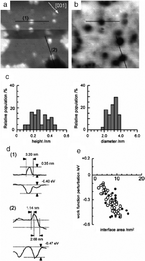
substrate [39,63]. Fig. 17(a)
and (b) show the topography and work function mapping of Pt
evaporated on a TiO
2
surface. As shown in the histogram, Fig. 17(c),
bright spots shown in Fig. 17(a) are Pt nanostructures with small
range of heights (0.12–0.48 nm, mean
= 0.30 nm) and diame-
ters (2–4 nm, mean
= 3.2 nm). In Fig. 17(b), the brighter areas
correspond to larger work functions. The work function on a Pt
nanostructure is smaller than on the supporting material, TiO
2
.
The authors think the electric dipole formation, due to the elec-
tron charge transfer from Pt nanostructures to the TiO
2
substrate,
causes work function differences between Pt nanostructures and
the TiO
2
surface. Fig. 17(e) shows the work function on the Pt
W. Melitz et al. / Surface Science Reports 66 (2011) 1–27 13
Fig. 14. The topography and work function images of UHV-cleaved KCl, surface
with different coverages of Au. Topography, (a), (c), and (e), and simultaneously
recorded surface potential images, (b), (d), and (f), of the clean KCl(001) surface,
(a) and (b), the same surface after a deposition of 0.04 ML Au at room temperature,
(c) and (d), and 1.44 ML of Au at 200
°C, (e) and (f). The clean surface was prepared
by UHV cleaving and annealing at 120
°Cfor2h.
Source: Adapted from [53].
nanostructures decreases as the interface area between Pt nanos-
tructures and supporting TiO
2
substrate increases. The linear de-
pendence of the work function on the interface area is similar
Fig. 16. Examples for charge transfer of Au atoms. (a) The frequency shift (f )
measured as a function of the voltage above Au
−
and Au
0
. Both measurements
are performed without moving the tip. After measuring
f (V ) above Au
−
, the
charge state is switched to Au
0
by applying a bias pulse of −1 V for a few seconds.
Parabolic fits and corresponding parabolic peaks are indicated. Scanning tunneling
microscopy images before (b) and after (c) the
f (V ) measurements confirm the
charge-switching event and show that the switched Au atom has maintained its
lateral position.
Source: Adapted from [58].
for terrace areas and step edge areas, as shown in Fig. 17(e).
Individual Pt adatoms and Na adatoms donate electrons to the
Fig. 15. A schematic diagram of AFM measurement and frequency shifts of Au adsorbed on NaCl/Cu(111). (a) Model geometry of the experimental setup for the AFM
measurements of Au/NaCl. Au, Cl
−
, and Na
+
are colored gold, green, and light blue, respectively. (b) Frequency shifts recorded in a constant height mode (z = 5.0Å, V =
−
5 mV, and A = 0.3 Å). (c) Line scan of the frequency shift through the center of Au
0
and Au
−
atoms shown in (b). The color scale in (c) corresponds to the f values, in
a three-dimensional representation of the cut along the line profile. (For interpretation of the references to colour in this figure legend, the reader is referred to the web
version of this article.)
Source: Adapted from [58].
14 W. Melitz et al. / Surface Science Reports 66 (2011) 1–27
Fig. 17. Examples for charge transfer in Pt nanostructures. (a) Topography and
(b) work function mapping of Pt evaporated onto a TiO
2
surface. (c) Distribution
of the heights and diameters of the Pt nanostructures formed on the terraces. (d)
Cross-sections obtained along the lines in images (a) and (b). (e) Deviation of the
work function of the Pt nanostructures on the TiO
2
surface, plotted as a function of
the nanostructure/TiO
2
interface area. Open and filled circles are obtained on the Pt
nanostructures formed on terraces and steps edges, respectively.
Source: Adapted from [39].
TiO
2
substrate [39,63]. Cl adatoms accumulate electrons from the
TiO
2
substrate [64].
Recently, Glatzel et al. demonstrated the contacting of sin-
gle molecular structures assembled on insulating surfaces by a
metallic nanostructure, a major step toward functional molecular
assemblies, providing possibilities to study molecular conduc-
tance [65]. KPFM results showed surface potential differences,
with nanometer resolution, between metallic nanostructures,
molecules, and the supporting insulating surface, were a function
of the local surface potential and the local dipole moment. With
further extension, charges can be added or removed at specific
sites of the molecules with the metallic terminals. Subsequently,
the whole molecule or molecular network can be characterized by
KPFM to investigate the charge transport [66].
3.2. Characterization of electrical properties on semiconductor nanos-
tructures
3.2.1. KPFM on semiconductor surfaces
The published reports on atomic-resolution KPFM on semicon-
ductor surfaces is dominated by Si surfaces [19,20,24,26,37,42,67]
but also include other surfaces such as TiO
2
[16,22,39], GaAs [68]
and InSb [23]. Properties, such as force distribution on a surface re-
construction, surface defects, phase state, and atomic composition,
have been investigated using KPFM.
3.2.1.1. Short-range force distribution on a surface reconstruction.
Atomic-resolution KPFM can map topography along with the
potential dependent forces, providing vital information on the
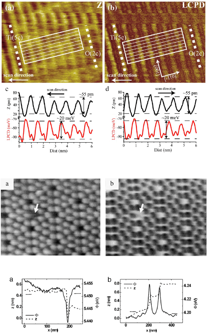
interaction properties of the surface atoms. Enevoldsen et al.
observed a 20 meV potential variation between the row and trough
of a TiO
2
(110) surface, as seen in Fig. 18 [16]. AM mode KPFM
with a 70 kHz Pt/Ir coated cantilever was used to achieve atomic
resolution. The row spacing on the TiO
2
(110) was measured as
∼1 nm. The LCPD profile shows a two-peak pattern. The large peak
indicates the attractive force to the five-fold coordinated Ti [Ti(5c)]
surface atoms. The dark feature is the repulsive force with the
two-fold coordinated O [O(2c)] row atoms. KPFM was employed
to resolve the row/trough structures on InSb [23] and InAs. The
short-range force on semiconductor surfaces is smaller than on
ionic solids, so the LCPD signal will be smaller. Krok et al. studied
InSb(001) surfaces and observed a 5 meV dip on the In rows [23].
To obtain the row-trough resolution for InSb(001), a 111 kHz Si
cantilever is used in FM mode. InSb has a row-trough structure
(row distance
∼1.7 nm) and a dip in the LCPD at the In row.
3.2.1.2. Surface defects. One of the most interesting and poten-
tially useful applications of the atomic-resolution KPFM is the vi-
sualization of single defects or step edges on the surface. Using
atomic-resolution KPFM, single vacancy defects can be imaged di-
rectly. KPFM can provide an insight into the electronic properties
of defects on the semiconductor surface. Shiota et al. observed a
vacancy defect on Si(111)-(7
× 7) with atomically-resolved KPFM
images, shown in Fig. 19 [38]. The potential energy of the corner
hole (arrow in Fig. 19)is61
±9 meV higher than the corner adatom
and 77
± 5 meV higher than the center adatom. The vacancy has
dangling bonds, which increases the short-range interaction with
the tip, causing an increase in the LCPD.
KPFM can be used to study defects larger than vacancies, such as
step edges or grain boundaries. Glatzel et al. has observed a 15 meV
decrease and a 40 meV increase of the surface work function for
cleaved p-type and n-type GaAs(110) steps, respectively as seen in
Fig. 20 [50]. Glatzel et al. also measured a 130 meV decrease and a
40 meV increase of the surface work functions on cleaved p-type
and n-type GaP(110) steps, respectively [50].
KPFM can investigate the effects of surface band structure on
the charge state of semiconductor surfaces. For III–V semiconduc-
tors, the (110) orientation is a common surface for cleaved sam-
ples. The (110) surface of III–V semiconductors normally exhibits
flat band conditions. The surface work functions should be similar
to bulk values [69]. However, step edge traps or defects can intro-
duce mid-gap surface states, which influence the surface Fermi en-
ergy level. The change in the CPD reflects the direction and amount
of band bending caused by these surface states. The decrease of
the measured work function for p-type materials is consistent with
bands bending down, positioning the surface Fermi level in the
band gap. For midgap states in n-type materials, the bands bend
up to position the Fermi level in the band gap, thereby increasing
the surface work function. KPFM is well suited to study the effects
of surface defects on electronic properties with high spatial reso-
lution. KPFM studies on surface electronic states have application
in the development of devices with large surface property effects,
such as laser diodes or solar cells.
W. Melitz et al. / Surface Science Reports 66 (2011) 1–27 15
Fig. 18. Atomic-resolution KPFM image of TiO
2
(110) surface. (a) Topography (Z) and (b) LCPD of TiO
2
(110), image size 10 × 8nm
2
. (c) Line scan average of topography
and LCPD indicated on image as rectangle box.
Source: Adapted from [16].
Fig. 19. Atomic-resolution KPFM images of Si(111)-(7 × 7) with vacancy. (a) Topography (b) LCPD images of the Si(111)-(7 × 7) surface with 7 × 10 nm
2
scan size.
Source: Adapted from [38].
Fig. 20. Line profiles of topography (dashed line) and work function (solid line) measured by KPFM through a atomic step on (a) p-type and (b) n-type GaAs(110) surface,
respectively. A 15 meV decrease and a 40 meV increase of the surface work function are observed for cleaved p-type and n-type GaAs(110) steps.
Source: Adapted from [50].
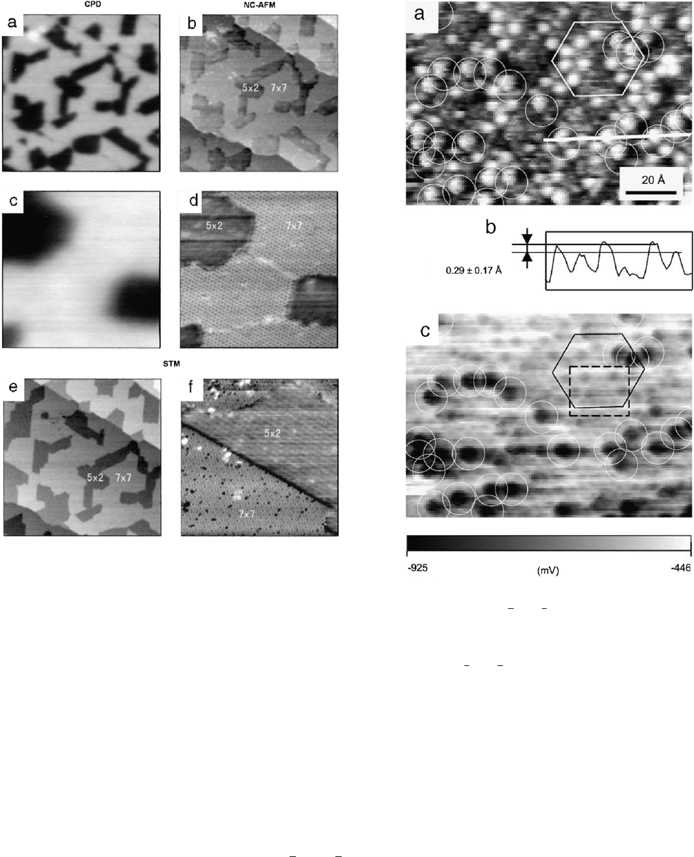
3.2.1.3. Reconstruction identification. The high-resolution KPFM
has been used for identification and comparison of different sur-
face reconstructions on a semiconductor surface. A 0.5 eV poten-
tial difference is measured between mixed Au/Si(111)-(7
×7) and
(5
× 2) surface reconstructions [24]. Fig. 21(a) and (b) shows
the 500
× 500 nm
2
CPD and topography of Au/Si(111) mixed
(7
× 7) and (5 × 2) surfaces. Initially, the reconstruction phases
are identified, as seen in Fig. 21(e) and (f), using scanning tun-
neling microscopy (STM). The position of the Fermi energy level
at the surface is dependent on the surface electronic states. Dif-
ferent surface reconstructions induce different surface electronic
states, resulting in different Fermi energy levels on the surface.
16 W. Melitz et al. / Surface Science Reports 66 (2011) 1–27
Fig. 21. KPFM and STM images of a mixed Si surface with (7 × 7) and (5 × 2)
reconstructions. 500
× 500 nm
2
(a) CPD (b) topography images of the Au/Si(111)
mixed (7
× 7) and (5 × 2) surface. 100 × 100 nm
2
(c) CPD (d) topography images
on the same surface. The (7
× 7) reconstruction has a 0.5 eV higher CPD than the
(5
×2) reconstruction. (e) 500 ×500 nm
2
(f) 50 ×50 nm
2
STM images on the same
surface showing clear surface reconstruction.
Source: Adapted from [24].
Surface dipoles can also introduce a change in the measured CPD.
Similar work has been reported on clean Si(111), showing a 0.11 eV
difference between the (7
× 7) and (1 × 1) mixed surface recon-
structions [67]. KPFM, in combination with other surface analysis
techniques, can help separate the different electrical effects of the
surface reconstruction on the measured CPD.
3.2.1.4. Atom identification. Okamoto et al. prepared a mixed Si–Sb
surface reconstruction and distinguished different surface atoms
based on their various tip interaction strengths [20]. This work is
the first experimental result using KPFM for atom identification.
The combination of topography and CPD image provides a clear
distinction between different atoms, difficult to extract from
topography imaging alone. For example, Sb is deposited on Si(111)
and annealed to achieve the Sb induced Si(111)-
(5
√
3 × 5
√
3)
surface reconstruction, (Fig. 22). In Fig. 22(a), the topography
image shows two types of bright spots on the surface. The two
bright spots show a slight height difference of 0
.29±0.17 Å. The Si
adatoms (circled adatoms) are the bright spots in the topography.
A CPD image of the same surface clearly distinguishes between the
two types of adatoms as seen in Fig. 22(c). The circled adatoms,
corresponding to lower CPD, are Si, while the other adatoms
Fig. 22. KPFM images of mixed Sb–Si surface. (a) 121 × 85 Å
2
topography image
of the Sb induced Si(111)-
5
√
3 × 5
√
3
surface reconstruction. Circles indicate
the Si adatoms which are 0
.29 ± 0.17 Å higher than the Sb adatoms. The hexagon
indicates the unit cell. (b) Topography line scan illustrating the height difference
between the two types of adatoms. (c) CPD image of the sample location on the Sb
induced Si(111)-
5
√
3 × 5
√
3
.
Source: Adapted from [20].
are Sb. The potential difference between the Si and Sb adatoms
is 0.2 eV. The measured difference between Si and Sb disagrees
with theoretical work: The Sb state should be 0.6 eV below the Si
adatom. This discrepancy sparked the discussion of the influence
of the short-range forces involved in atomic-resolution KPFM.
3.2.2. Adsorbates on semiconductor surfaces
One of the simplest applications of high-resolution KPFM is
the observation of the interaction properties of an adsorbate on
a surface. The potential change provides information about the
tip–adsorbate interactions relative to the tip–surface interactions,
indicating electron exchange or dangling bonds. An average CPD
value is also measured, representing the true surface potential.
Kitamura et al. deposited Au on Si(111)-(7
× 7), and the
Au adsorbates showed a higher potential (lower work function)
than the clean Si(111)-(7
× 7) surface [26]. The potential change
corresponds to the change in tip–sample interaction of the Si and
Au surface atoms. The Si adatoms on the surface have dangling
W. Melitz et al. / Surface Science Reports 66 (2011) 1–27 17
Fig. 23. KPFM images of Pt on TiO
2
. (a) Topography and (b) work function mapping
of Pt on TiO
2
. Image size 10 ×10 nm
2
(c) Cartoon mapping of the surface indicating
the two different bonding sites (white circles site A and dark circles sites B). (d) Line
profiles indicating the potential and height differences of the two sites. (e) Height
and (f) work function decrease histograms of (a) and (b), respectively.
Source: Adapted from [39].
bonds interacting with the apex of the tip. The metal clusters have
delocalized electrons, reducing the tip interaction strength, which
reduces the work function.
Ag was also deposited on Si(111)-(7
× 7), and a potential
dependence on the size of the Ag aggregates was observed [24].
The Ag ‘‘clusters’’ (aggregates smaller than a few nanometer) show
a work function 10 meV smaller than the clean Si surface. When Ag
‘‘islands’’ are formed (aggregates larger than a few nanometers),
the work function is approximately 10 meV higher than the
measured clean surface. The islands are small crystallites with
(111) plane orientation on the Si substrate, whereas the clusters
are polycrystalline Ag, which do not have an ordered surface. The
work function difference is caused by the difference in electronic
properties of the surfaces.
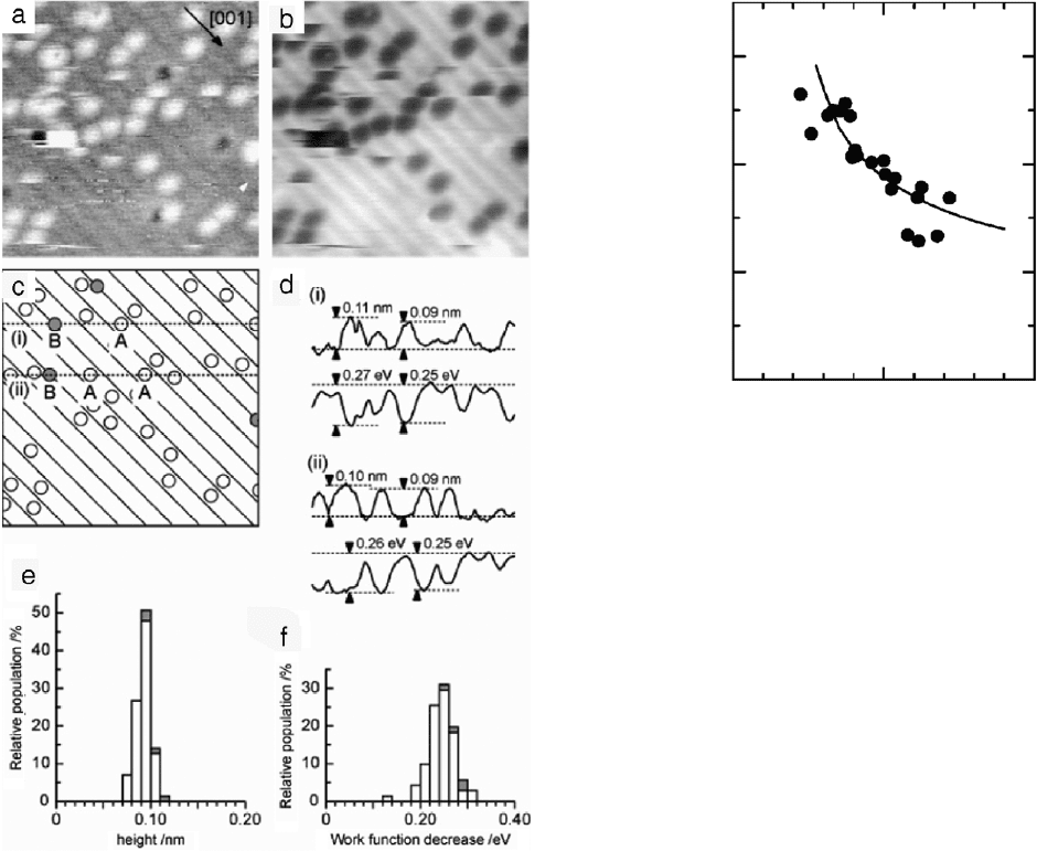
The high-resolution work function mapping can be used to
distinguish differences in structures of adsorbates on the surfaces.
Pt on TiO
2
(110) shows a work function decrease between 0.24 and
0.28 eV [39]. Fig. 23 shows the work function mapping of the Pt
adatoms on the clean surface TiO
2
(110) surface. The streaks were
reported as thermal diffusion of the adatoms on the surface. Two
different bonding sites were identified and characterized. Site A is
the Pt on the Ti row atom and site B is Pt on O vacancies. The work
0
05
Dot Height (nm)
CPD (eV)
10
-0.2
-0.4
-0.6
Fig. 24. The height dependence of the CPD of InAs QDs. Filled circles represent
collected data of the measured CPD of different InAs QDs on GaAs(001) surface. The
solid line shows calculated values using a quantum disk model.
Source: Adapted from [76].
function difference between the two sites is 0.02 eV, consistent
with simple bonding models. For site B, more electron transfer
causes a lower work function.
3.3. Nano-scale electrical properties characterization in devices
KPFM has demonstrated a unique usefulness in characterizing
the properties of various electronic devices, because KPFM
can correlate potential distribution with device structures. The
versatility of KPFM is featured in studies of many devices; quantum
dots (QDs), electrical junctions, transistors, and solar cells. KPFM
is compatible with operational devices [70–74], allowing imaging
under different performance conditions. High energy resolution
KPFM can characterize the single electron trapping in a QD [75].
The influence of surface states changes with device types and
material types. Experiments are performed most commonly in air,
which can introduce surface states. For absolute work function
measurements, surface states will drastically change the measured
values. Air may also introduce other variables when the system
contains different materials. For example, the native oxide will
form with any exposure to air in a system containing InAlAs,
whereas GaAs is less reactive to air and might only generate surface
states.
Surface states in junctions of a single material can cause
a reduction in the measured CPD difference because of band
bending in each layer. For example, a p–n junction will show a
lower than expected built-in potential. However, after applying
an external bias, the full potential change is observable, with
little influence from the surface states. External biasing alters
the relative references within the device, creating a shift in the
measured CPD from the equilibrium state. Surface states will
influence measured values, but the changes from equilibrium to
excited will be insignificant.
3.3.1. Quantum dots
QDs are used in the development of static memory, lasers,
solar cells and many other applications. Studying QDs with
KPFM has a significant advantage over STM and photon based
methods, because KPFM provides the structure and the potential
of the QDs simultaneously. Yamauchi et al. observed a potential
dependence on the height of InAs QDs grown on GaAs(001), shown
in Fig. 24 [76]. The calculated CPD dependence on the QD size
using a quantum disk model (shown as the solid line in Fig. 23)
is consistent with experimental results. QDs ranging from 1.3 to
18 W. Melitz et al. / Surface Science Reports 66 (2011) 1–27
10.80.6
[μm]
[μm]
0.40.20
10.80.6
[μm]
0.40.20
0.00
[nm]
9.36
10.80.6
[μm]
0.40.20
66.28
[mV]
512.73
0.00
[nm]
7.65
1
0.8
0.6
0.4
0.2
0
[μm]
1
0.8
0.6
0.4
0.2
0
[μm]
1
0.8
0.6
0.4
0.2
0
10.80.6
[μm]
0.40.20
156.66
[mV]
429.70
[μm]
1
0.8
0.6
0.4
0.2
0
ab
cd
Fig. 25. Charging of Si QDs with KPFM. (a) Topography and (b) CPD images of Si QDs prior to charging. (c) topography and (d) CPD of Si QD after charging by biasing tip
with
−5V.
Source: Adapted from [75].
7.2 nm of height and 21.8 to 44.6 nm of width were observed. The
height increases with decreasing CPD (filled circles in Fig. 23). The
measured CPD includes the potential increase from the quantum
size effect. KPFM can explore the properties of the QD itself, while
revealing the QDs interactions with the sample surface.
Shusterman et al. investigated InSb QDs and their strain effects
on a GaAs surface [77]. Dark rings in the CPD appeared around the
InSb QDs. High-resolution TEM confirms the surrounding substrate
is strained. The potential change due to the straining of the GaAs
lattice, is observable because of the high spatial resolution of KPFM.
KPFM is used to investigate the detailed electrical properties
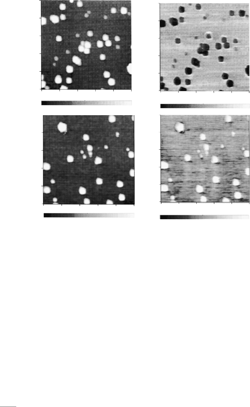
of QDs, particularly their charge states. Salem et al. observed the
potential change caused by the charging of Si QDs [75]. Si QDs
2–8 nm in diameter were deposited on SiO
2
. Fig. 25(a) and (b)
shows the topography and CPD of the uncharged QDs. Placing the
tip in contact with the QDs and applying a
−5 V bias, for 30 s,
charged the QDs. Fig. 25(c) and (d) shows the topography and
CPD change after charging of the QDs. The charged QDs shows an
increased CPD, while the substrate maintains the sample potential
around 300 mV. The estimated potential change due to charging of
the QD is [75]:
V =
(
ne)
2
q4πεd
, (3.1)
where d is the QD diameter, n is the number of injected electrons,
and
ε is the dielectric constant of silicon. Eq. (3.1) is based on the
expression for the conduction band energy of a QD after charging.
The QD’s diameter controls the amount of charge stored in the
QD. The CPD is consistent with the capturing of a single electron
for QDs with diameter less than 2.8 nm. QDs with 4.7–7.4 nm in
diameter have a CPD consistent with trapping of three electrons.
QDs with diameters 2.8–4.7 nm are expected to trap two electrons;
however, no QDs in that diameter range were observed. The results
illustrate how KPFM can be used to investigate electron charging
of QDs over various diameters. KPFM shows the added ability to
purposely alter electronic properties by providing a nano-scale
electrode. Electrons can be injected through QDs via the probe tip
during KPFM measurement.
3.3.2. Junctions and heterostructures
Prior to the invention of KPFM, KP had been used to characterize
electrical properties of junction devices [78–81]. In the last decade,
KPFM has become the preferred tool to study 2D potential profiles
in semiconductor junctions. Recently, KPFM has been recognized
as an exceptional tool to characterize p–n junctions [11,82–88],
p–i–n [89,90] and heterostructures [91–94], due to KPFM’s high
spatial resolution in measuring the surface potential. The impact
of surface properties increases as the devices scale down, due
W. Melitz et al. / Surface Science Reports 66 (2011) 1–27 19
0.6
Fig. 26. KPFM on a laser diode. (a) Measured CPD of InP/InGaAsP/InP p–i–n junction showing a 0.6 eV change between n-InP and p-InP and (b) electric field. (c) Calculated
potential and electric field profiles using ATLAS/BLAZE from SILVACO, Santa Clara, CA. The electric field is the first derivative of the potential profile.
Source: Adapted from [89].
Fig. 27. CPD of multi-junction GaAs samples. (a) Series of GaAs p–n junctions with and without external illumination. With illumination, a contrast is observed between
the different layers, and the baseline CPD is reduced to 0.5 eV from 0.7 eV. The baseline CPD is the background CPD level in the junctions. (b) Band diagrams illustrating the
charge separation of excited electron–hole pairs from the built-in electric field of the surface. Solid lines indicate the bands without illumination. The dashed lines indicate
the bands under illumination.
Source: Adapted from [82].
to surface-to-volume ratio increases. KPFM can be used to
measure accurately the surface band bending of scaled diodes and
heterostructures. KPFM is a passive technique, allowing the tip to
probe the surface without interfering with electronic properties.
Compatibility with illumination or external applied biases also
makes KPFM an attractive microscopy for junctions.
KPFM measurements are performed mostly on devices in air
or on devices exposed to air prior to scanning. Air exposure
introduces an interesting complexity to the interpretation of the
KPFM results, because adsorbates may introduce or passivate
surface states, causing surface band bending. KPFM is extremely
surface sensitive. Measured CPD in the presence of surface band
bending does not truly represent the bulk potential profiles [32].
In most bulk measurements of device structures, cleaving in UHV
avoids modification to the surface potentials from adsorbates or
oxide layers.
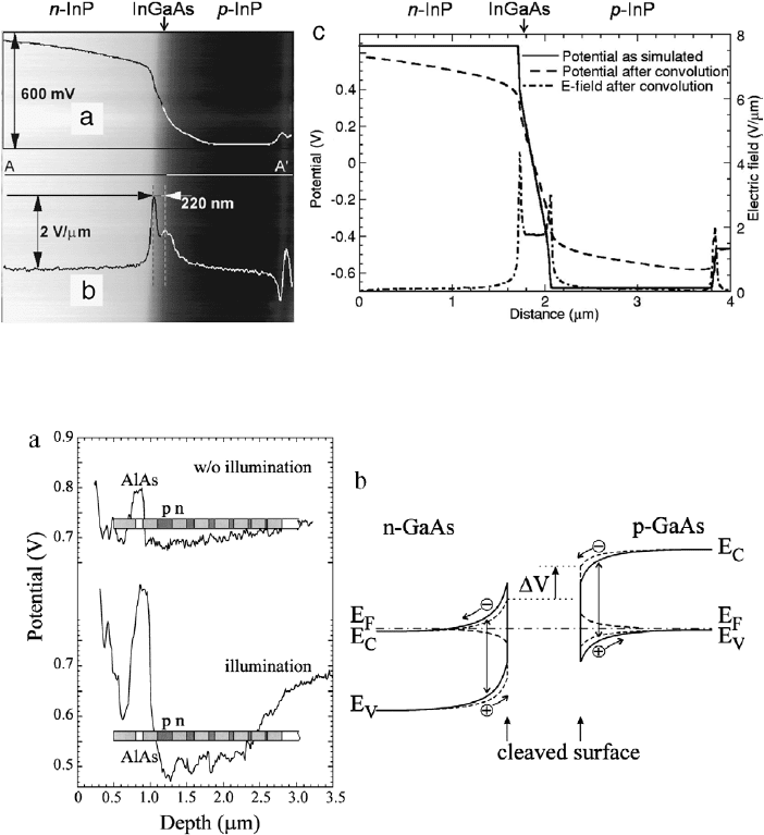
Robin et al. performed KPFM (in air) on a InP–InGaAsP p–i–n
laser diode [89]. Fig. 26(a) shows the measured CPD of the
p–i–n diode with 600 meV difference between p and n-type
InP. The expected potential difference is 1.3 eV. The calculated
potential and electric field profiles, shown in Fig. 26(b), are in good
agreement with the measured results, with the exception of the
magnitudes of the CPD. Surface states caused band bending, which
suppressed the magnitude of the CPD change.
KPFM is compatible with external illumination, which can help
probe the electronic states on the surface. Diodes are extremely
sensitive to excitation, and light may cause changes in the
measured CPD. Mizutani et al. observed that a multiple p–n GaAs
device under illumination has a baseline potential (the background
level of the CPD in the device region) of 0.5 eV compared to 0.7 eV
in dark conditions. An increase in contrast between device layers is
also seen in Fig. 27(a) [82]. Without illumination, the cleaved GaAs
surface shows little CPD difference between n-type and p-type,
because of surface states. All the measurements were performed
in air and the native oxide was expected to introduce surface
states. When illuminated, the electron–hole pairs were separated
by the electric field caused by the surface band bending. Holes will
accumulate at the surface for n-type and electrons for p-type, as
seen in Fig. 27(b). These accumulation layers will cause an increase
in the CPD contrast between the n-type and p-type layers.
Loppacher et al. also observed a contrast increase between
n-type and p-type Si under illumination [86]. The measured CPD
difference between n-type and p-type Si is 320 and 120 meV
for illuminated and dark conditions, respectively. The expected
difference is 0.8 eV, but the measured difference is only 0.2 eV. This
anomaly may imply that surface electronic states dominate the
measured CPD and that the illumination has insufficient intensity
20 W. Melitz et al. / Surface Science Reports 66 (2011) 1–27
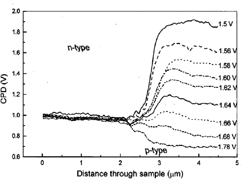
Fig. 28. CPD measurement on an operational GaP LED. Potential profiles of GaP
n–p junction under forward biases, from 1.5 to 1.78 V. The built-in potential of an
air cleaved GaP diode is expected to be 2 V, but only 1.2 V is measured by KPFM.
Source: Adapted from [84].
to saturate the surface states. External illumination on a p–n
junction increases the CPD contrast, because of the electrons or
holes accumulating at the surface.
Conversely, for quantum well structures, external illumination
causes a drop in the measured CPD because of charge screening.
Chavez-Pirson et al. observed a screening effect for an illuminated
n–i–p–i AlGaAs quantum structure [91]. Illuminating the structure
increases the baseline CPD about 70 meV and reduces the potential
contrast. A difference in band bending of n-type and p-type under
illumination causes the baseline increase. The contrast between
n-type and p-type layers in CPD is reduced, because a screening
of the electric fields at the junction occurs from the excited
electron–hole pairs. External illumination can help to suppress
surface states. However, illumination is not ideal for every system,
because the devices’ structure can have a larger dependence on the
photo-generated electron hole pairs than on the surface state.
The diffusion lengths of the photo-generated carriers have been
measured on a p–n junction by high-resolution KPFM. For GaP
p–n junctions, Meoded et al. measured hole diffusion lengths and
their dependence upon illumination intensity [87]. The intensity
of the illumination source was varied. The CPD profile is fitted to
the minority carrier continuity equation to determine the expected
diffusion lengths. The diffusion length increases with increasing
intensity and agrees with the theoretical diffusion lengths.
An external bias can be applied during KPFM measurements,
which provides data on junction properties in different modes
of operation. Shikler et al. measured the potential profile of an
operational light emitting diode (LED) under different applied
biases [11,84]. The built-in potential of an air-cleaved GaP diode
is expected to be 2 V, but only 1.2 V is measured by KPFM. The
decrease in built-in potential can also be explained by surface
states from native oxide formation. The surface states act as traps
for the majority carriers, which causes a depletion region, bending
the bands up and down for n-type and p-type, respectively. Fig. 28
shows the potential distribution of the GaP diode over a range of
applied biases. The key feature is the range of applied biases is
0.28 V, while the range of measured CPD in the p-type region is
1.2 V. The increase in built-in potential is photo-voltage induced
from recombination of internal emission photons. When applying
an external illumination to the diode under different biases, the
surface photo-voltage increases with intensity of the external
source.
Quantum wells or heterostructures for applications in lasers
diodes and photodetectors can be investigated using KPFM.
For laser diodes, the measurement of potential changes during
operation is extremely useful for determining causes of decreased
performance. Ideally, the entire voltage drop should span the active
region of the laser diode. Lévêque et al. observed only 30% of
the applied bias drops across the active region of an air exposed
GaSb laser [94]. The reduction in the potential drop across the
active region contributed to a significant voltage drop across the
substrate at positive biases and a non-negligible voltage drop
across the substrate–cladding interface. For negative biases, a
lower voltage drop was measured across the substrate, with a
significant voltage drop across the cladding layer. Determining
the sources of voltage losses assists designers to improve the
performance of laser diodes.
High-resolution KPFM can be applied even to nano-scale
heterostructure features to observe variations in CPD. Schwarzman
et al. measured the CPD of a GaAsP/InGaAs multi-quantum well
solar cells cleaved in situ [93]. The 8 nm quantum wells show a
barrier height of 10 meV with 45 nm barrier widths. Charging
of surface states causes a reduction of CPD difference of n and
p
+ regions from 1.4 to 0.5 eV.
KPFM also has been used to investigate the mechanisms of crit-
ical failure or burnout of a laser diode during operation. Ankudi-
nov et al. investigated a InGaAs/AlGaAs/GaAs heterostructure laser
diode cleaved in air with KPFM under different applied biases [90].
Surface charge screening, causing a reduction in the measured volt-
age drop, occurs in equilibrium to 200 meV from the expected
voltage drop of 1.5 eV. The CPD of the laser diode from 0 to
1.7 eV forward biases is shown in Fig. 29(c). At the higher biases, a
bump can be seen (indicated by arrow) in the surface voltage drop
[Fig. 28(d)]. This bump is a potential drop across the buffer–emitter
interface. Parasitic power sinks can cause failure of laser diodes.
When the laser diode is biased with high injection currents, the
buffer–emitter interface heats and appears to melt, destroying the
laser diode. The advantage of KPFM for studying failure mecha-
nisms is the measurement of the device during operation.
KPFM has been shown to be a powerful technique for studying
semiconductor heterostructures. Heterostructures can also be
used for calibrating the spatial and energy resolution of KPFM. The
spatial resolution can be measured directly in the CPD image by
having a series of quantum wells with varying thicknesses [92,95].
Usunami et al. performed KPFM on cleaved GaAs/AlAs and
InAlAs/InGaAs heterostructures, in air, and were able to resolve a
20 nm layer [95]. Fig. 30 shows the measured topography and CPD
of InAlAs layers ranging from 20 to 200 nm thicknesses sandwiched
between 200 nm layers of InGaAs.
The challenge for investigating junctions or heterostructures is
overcoming surface state effects. Since nearly all measurements
are performed in air, which induces native oxide formation.
KPFM is an attractive measurement technique for junctions
and heterostructures because of the plethora of experiments
compatible with KPFM. KPFM has the significant advantage of
high spatial resolution for operational devices, yet does not
always accurately represent the bulk potential values. The key
to accounting for surface states is to integrate the KPFM with
other techniques to provide bulk properties. KPFM has great
value for measuring the electronic structures of junctions and
heterostructures, including band alignment, failure mechanisms,
and surface electronic changes from absorption of photons.
3.3.3. Transistors
Experimental techniques providing valuable electrical, me-
chanical and processing properties are critical to the development
of FETs (field effect transistors). KPFM provides a two-dimensional
profile of surface potentials, ideal for transistor structures. KPFM
identifies features causing a decrease of device performance,
such as high contact resistances from Schottkey barriers [70].