Middleton W.M. (ed.) Reference Data for Engineers: Radio, Electronics, Computer and Communications
Подождите немного. Документ загружается.

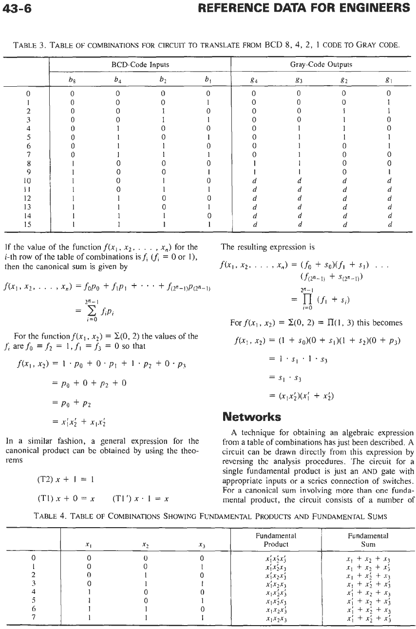
43-6
0
1
2
3
4
5
6
7
8
9
10
11
12
13
14
15
REFERENCE
DATA
FOR
ENGINEERS
BCD-Code
Inputs Gray-Code Outputs
b8
b4
b2
bl
g4
g3
g2
gl
0 0
0
0
0 0 0 0
0
0
0
1
0
0 0
1
0
0
1
0
0 0
1
1
0
0
1 1
0 0
1
0
0
1
0
0
0
1 1
0
0
1
0
1
0
1
1
1
0
1
1
0
0
1
0
1
0
1
1
1
0
1
0
0
1
0
0
0
1 1
0 0
1
0
0
1 1
1
0
1
1
0
1
0
d
d d
d
I
0
1
1
d d d
d
1
1
0
0
d d
d
d
1
1
0
1
d d d d
1
1
1
0
d d
d
d
1
1
1
1
d
d
d d
TABLE
3.
TABLE
OF
COMBINATIONS
FOR
CIRCUIT
TO
TRANSLATE
FROM
BCD
8,
4,
2,
1
CODE
TO
GRAY CODE.
0
1
2
4
6
3
5
7
0
0
0
xi.;.;
XI
+
x2
+
x3
0
0
1
x;x;x3
XI
+
x2
+
x;
0
1
0
X;X2X;
XI
+
x;
+
Xj
x,
+
x;
+
x;
1
0
0
xlx;x;
x;
+
x2
+
x3
xi
+
x2
+
x;
xi
+
x;
+
x3
1
1
0
XIX24
xi
+
x;
+
x;
0
1 1
x;x2x3
1
0
1
xlx;x3
1
1
1
xIx2x3
2"-
1
i=O
=
C
fipi
=
n
(fl
+
Si)
i=O
Forf(xl,
x2)
=
8(0,
2)
=
n(l,
3)
this becomes
f(Xl>
x2)
=
(1
+
so)@
+
s,)(l
+
s2)(0
+
P3)
For the functionf(x,
,
x2)
=
8(0,2)
the values
of
the
fi
arefo
=f2
=
l,fl
=f3
=
0
so
that
=
Po
+
P2
=
x;x;
+
XI.;
Networks
A
technique for obtaining an algebraic expression
from a table of combinations has just been described.
A
circuit can be drawn directly from this expression by
reversing the analysis procedures. The circuit for a
single fundamental product is just
an
AND
gate with
appropriate inputs or a series connection
of
switches.
For a canonical
sum
involving more
than
one funda-
mental product, the circuit consists
of
a number
of
In
a similar fashion, a general expression for the
canonical product can be obtained by using the theo-
rems
(T2)
x
+
I
=
1
(Tl)x+O=x (Tl')x.l=x
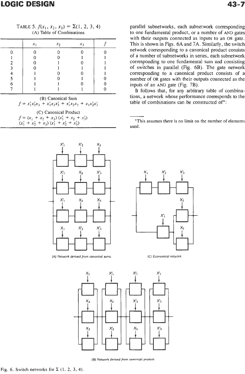
TABLE
4.
TABLE
OF
COMBINATIONS SHOWING FUNDAMENTAL PRODUCTS
AND
FUNDAMENTAL SUMS
I I
Fundamental Fundamental
x2
x3
Product
Sum
LOGIC
DESIGN
43-7
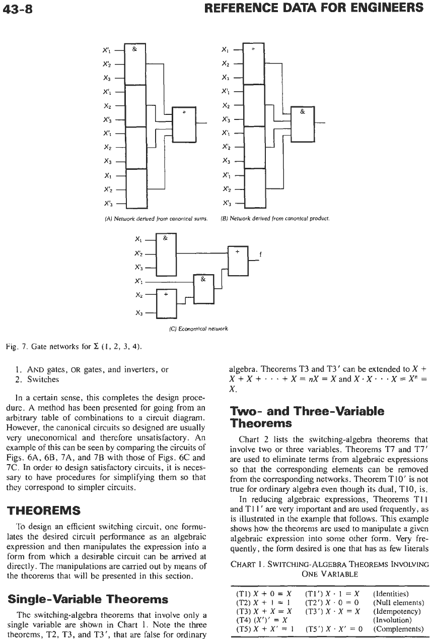
TABLE
5.
f(x,,
x2, x3)
=
2(1,
2,
3,
4)
(A)
Table
of
Combinations
(B)
Canonical Sum
(C) Canonical
Product
f
=
x;x;x,
+
x;x*x;
+
x;x2x3
+
x,xix;
f=
(Xi
+
x*
+
Xj)
(x;
+ x2
+
x;,
(x;
+
xi
+
x3) cx;
+
xi
+
x;,
f
(A)
Network derived
from
canonical sums.
XI
X'1
1
1
parallel subnetworks, each subnetwork corresponding
to one fundamental product, or a number
of
AND
gates
with their outputs connected as inputs to an
OR
gate.
This is shown in Figs.
6A
and
7A.
Similarly, the switch
network corresponding to a canonical product consists
of a number
of
subnetworks in series, each subnetwork
corresponding to one fundamental
sum
and consisting
of switches in parallel (Fig.
6B).
The gate network
corresponding to a canonical product consists of a
number
of
OR
gates with their outputs connected as the
inputs
of
an
AND
gate (Fig.
7B).
It follows that, for any arbitrary table of combina-
tions, a network whose performance corresponds to the
table
of
combinations can be constructed
of*:
*This
assumes
there
is
no
limit
on
the
number
of
elements
used.
(C)
Economical
network.
(B)
Network derlved
from
canonlcal
product.
Fig.
6.
Switch networks
for
(1,
2,
3,
4).
43-8
REFERENCE
DATA
FOR ENGINEERS
(A)
Network derlued
from cononicol
sums
XI
x2
x3
X'1
XZ
x;
X'I
XI2
x3
X'I
XI2
X'3
(E)
Network derlued
from
canonlcol
product
XI
x2
:wf
x3
(Cj
Economical
network
Fig.
7.
Gate
networks
for
2
(1,
2,
3, 4).
1.
AND gates,
OR
gates, and inverters, or
2.
Switches
In a certain sense, this completes the design proce-
dure. A method has been presented for going from an
arbitrary table of combinations to a circuit diagram.
However, the canonical circuits
so
designed
are
usually
very uneconomical and therefore unsatisfactory. An
example of this can be seen by comparing the circuits of
Figs. 6A, 6B, 7A, and 7B with those
of
Figs. 6C and
7C. In order to design satisfactory circuits, it is neces-
sary to have procedures for simplifying them
so
that
they correspond to simpler circuits.
THEOREMS
To
design an efficient switching circuit, one formu-
lates the desired circuit performance as an algebraic
expression and then manipulates the expression into a
form from which a desirable circuit can be arrived at
directly. The manipulations are carried out by means of
the theorems that will be presented in this section.
algebra. Theorems T3 and T3' can be extended to X
+
X
+
X
+
. . .
+
X
=
nX
=
XandX.X.
.
*X
=
X"
=
X.
Two-
and
Three-Variable
Theorems
Chart
2
lists the switching-algebra theorems that
involve two or three variables. Theorems T7 and T7'
are used to eliminate terms from algebraic expressions
so
that the corresponding elements can be removed
from the corresponding networks. Theorem T10' is not
true for ordinary algebra even though its dual, T10, is.
In reducing algebraic expressions, Theorems TI
1
and T1
1
'
are very important and are used frequently, as
is illustrated in the example that follows. This example
shows how the theorems are used to manipulate a given
algebraic expression into some other form. Very fre-
quently, the form desired is one that has as few literals
CHART
1.
SWITCHING-ALGEBRA THEOREMS INVOLVING
ONE VARIABLE
Single-Variable Theorems
The switching-algebra theorems that involve only a
single variable are shown in Chart
1.
Note the three
theorems, T2, T3, and T3', that are false for ordinary
(Tl)
X
+
0
=
X
(T2)
X
+
1
=
1
(T3)
X
+
X
=
X
(T4)
(X')'
=
X
(Involution)
(T5)
X
+
X'
=
1
(Tl')
X
.
1
=
X
(T2')
X
.
0
=
0
(T3')
X
.
X
=
X
(T5')
X .
X'
=
0
(Identities)
(Null
elements)
(Idempotency)
(Complements)
CHART 2. SWITCHING-ALGEBRA THEOREMS INVOLVING
TWO
OR
THREE
VARIABLEs
(T6) X+Y=Y+X (T6’) XY
=
Yx
(Commutative)
(T7) X+XY=X (T7’) X(X
+
Y)
=
x
(Absorption)
0-8)
(X
+
Y‘)Y
=
XY (T8’) XY’
+
Y
=
x+
Y
(T9)
(T9’) (XY)Z
=
X(YZ)
=
XYZ
(Associative)
(T10)
(T10’)
(Distributive)
(TI
1)
(T11
’)
(Consensus)
(TI21
(X+ Y)
+
z
=
x
+
(Y
+
2)
=x
+
Y
+
z
XY
+
xz
=
X(Y
+
Z)
(X
+
Y)(X
+
2)
=
x
+
YZ
(X
+
Y)(X’
+
Z)(Y
+
Z)
=
(X
+
Y)(X’
+
Z)
XY
+
X’Z
+
YZ
=
XY
+
X’Z
(X
+
Y)(X’
+
2)
=
xz
+
X’Y
occurring as possible. The number of literal occur-
rences corresponds roughly to the number of gate inputs
in a gate network.
Theorem T12 has no dual (T12’), for the dual would
be identical with the original theorem.
Example
By use of the theorems, the expression
(c‘
+
abd
+
b‘d
+
a’b)(c
+
ab
+
bd)
is
to
be shown equal to
b(a
+
c)(a’
+
c’)
+
d(b
+
c)
(c’
+
abd
+
b’d
+
a‘b)(c
+
ab
+
bd)
c’(ab
+
bd)
+
c(abd
+
b’d
+
a’b)
abc’
+
bc‘d
+
abcd
+
b’cd
+
a‘bc
abc’
+
abcd
+
bc’d
+
a’bc
+
b’cd
ab@’
+
cd)
+
bc’d
+
a‘bc
+
b’cd
ab@’
+
d)
+
bc’d
+
a‘bc
+
b’cd
ab@’
+
d)
+
bc’d
+
a‘bc
+
a’bd
+
b’cd
abc’
+
abd
+
bc’d
+
a’bc
+
a‘bd
+
b’cd
(abd
+
a’bd)
+
abc’
+
bc’d
+
a’bc
+
b’cd
bd(a
+
a‘)
+
abc‘
+
bc’d
+
a’bc
+
b‘cd
bd(1)
+
abc’
+
bc’d
+
a’bc
+
b’cd
bd
+
abc’
+
bc’d
+
a’bc
+
b’cd
bd
+
bc‘d
+
abc’
+
a’bc
+
b’cd
(T7)
(T6),(T10)
(T8’)
bd
+
abc’
+
a’bc
+
b’cd
d(b
+
b‘c)
+
abc’
+
a’bc
d(b
+
c)
+
abc‘
+
a’bc
(T10)
d(b
+
c)
+
b(ac‘
+
a’c)
d(b
+
c)
+
b(a
+
c)(a’
+
c’)
n-Variable Theorems
The switching-variable theorems that involve an
arbitrary number of variables are shown in Chart 3.
Three of these theorems (T13, T13’, and T14) cannot
be proved by perfect induction. For these theorems, the
proofs require the used of finite induction.
*
Theorems
T 1 3 and T
1
3
‘
are proved by first letting
n
=
2 and using
perfect induction to prove their validity for this special
case. It is then assumed that the theorems are true for
n
=
k,
and this is shown to imply that they must then be
true for
n
=
k
+
1. This completes the proof, the details
of which are given in the reference. Theorem T14 is
proved by using Theorems T13 and T13’ along with the
fact that every function can be split into the sum of
several functions or the product of several functions. By
successively splitting the function into subfunctions and
using T13 and T13’, it is possible to prove T14.
Theorem T14, which is a generalization of T13,
forms the basis of a method for constructing comple-
mentary networks. Two networks having outputs
TI
and
T2
are said to be
complementary
if
T,
=
T;.
The
complementary network for any given network can be
designed by writing the output,
TI,
for the first net-
work, then forming
7’;
by means of T14, and then
designing a network having output
T;.
For example,
if
TI
=
(x
+
y)[w(y’
+
z)
+
xy],
then
Ti
=
x’y‘
+
It was pointed out in connection with Figs.
6
and
7
that the canonical networks are generally uneconomi-
cal. By manipulating the canonical sum or product with
the aid of the theorems just presented, it
is
usually
possible to obtain algebraic expressions that correspond
to more economical networks than the canonical net-
works. The following example shows how this is done
(w’
+
yz‘)(x’
+
y’).
-
*See reference
2.
43-
10
REFERENCE DATA FOR ENGINEERS
CHART
3.
SWITCHING-VARIABLE
THEOREMS
INVOLVING
n
VARIABLES
(DeMorgan’s theorems)
(T13)
(T13’)
(XI
i-
X2
+
.
.
‘
f
Xn)’
=
x;X;
.
.
.
XA
(XIX,
.
‘
X,)’
=
Xi
f
Xi
+
’ ’
‘
f
XL
(Generalized DeMorgan’s theorem)
f(X,, X,,
.
.
,
,
X,,
+,
.)‘
=f(X;,
Xi,
. . .
,
XL,
.,
+)
(Expansion
theorem)
f(X,, X,,
.
.
.
,
x,)
=
X~f(l,
x2,
.
.
.
,
x,)
+
x;f(o,
xz,
. . .
2
xn)
f(X,, X,,
. .
.
,
X,)
=
[xi
+f(o,
Xz,
.
.
.
,
x,)l[x; ff(1, xz,
.
.
.
,
Xn)]
(T14)
(T15)
(T15‘)
for the networks of Figs.
6
and
7.
The final expressions
correspond to the networks of Figs. 6C and
7C.
f=x;x;x, +x;x,x; +x;x,x, +x,x;x;
f=x;x;x, +x;x2x, +x;x2x; +x,x;x;
f=x;x~x3+x;x,x3 +x;x,x, +x;x,x; +x,x;x;
f=x;x,(x;+x,) +x;x,(x,+x;) +x,x;x;
f=x;x,(l)
+XiX2(1)
+x,x;x;
,f=XiX,
+XiX2
+x,x;x;
f=x;
(X3
+X2)
+x,x;x;
Many of the theorems of ordinary algebra are also
valid for switching algebra. One that is not is the
cancellation law. In ordinary algebra, it follows that
X
=
Z
if
X
+
Y
=
Y
+
Z.
In switching algebra, this is not
true. For example, it is generally true that
X
+
XY
=
X
+
0,
but it is not necessarily true that
XY
=
0.
This can
be easily verified by writing out the tables of combina-
tions forf!
(X,Y)
=
X
+
XY,f2
(X,Y)
=
X
+
0,
andf3
(X,Y)
=
XY.
Similar remarks apply to the situation in
which
XY
=
XZ
does not imply that
Y
=
Z.
GENERAL
GATE
NETWORKS
The previous discussion of gate networks in this
chapter has been concerned solely with networks con-
structed of
AND
gates and
OR
gates. This can be
considered only an introduction to the topic of gate
networks, for other types of gates are equally important.
In this section, networks with other types of gates will
be considered.
Any arbitrary switching function can be realized by a
network of
AND
gates,
OR
gates, and inverters. A
natural question to ask in this connection is whether all
three types of elements are necessary. Inverters are
required if the inputs to the network consist of signals
representing the input variables but not of signals
representing the complements of the input variables.
The situation when signals representing the comple-
ments are available
is
called
double-rail logic,
and when
the complements are not available, the term
single-rail
is used. Both techniques are employed, but for the
purposes of the present discussion it will be assumed
that complements are not directly available (single-rail
logic). The functionf(x)
=
x‘
cannot be realized by a
network of
AND
gates and
OR
gates only.
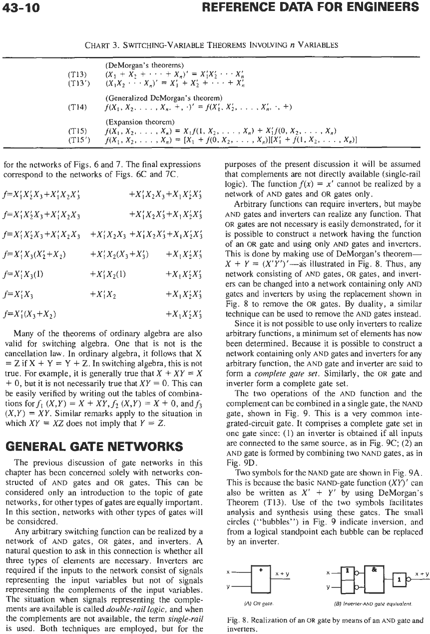
Arbitrary functions can require inverters, but maybe
AND
gates and inverters can realize any function. That
OR
gates are not necessary is easily demonstrated, for it
is possible to construct a network having the function
of an
OR
gate and using only
AND
gates and inverters.
This is done by making use of DeMorgan’s theorem-
X
+
Y
=
(X’Y’)‘-as
illustrated in Fig.
8.
Thus, any
network consisting of
AND
gates,
OR
gates, and invert-
ers can be changed into a network containing only
AND
gates and inverters by using the replacement shown in
Fig.
8
to remove the
OR
gates. By duality, a similar
technique can be used to remove the
AND
gates instead.
Since it is not possible to use only inverters to realize
arbitrary functions, a minimum set
of
elements has now
been determined. Because it is possible to construct a
network containing only
AND
gates and inverters for any
arbitrary function, the
AND
gate and inverter are said to
form a
complete gate
set.
Similarly, the
OR
gate and
inverter form a complete gate set.
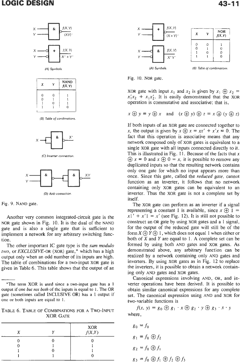
The two operations of the
AND
function and the
complement can be combined in a single gate, the
NAND
gate, shown in Fig.
9.
This is a very common inte-
grated-circuit gate. It comprises a complete gate set in
one gate since:
(1)
an inverter is obtained if
all
inputs
are connected to the same source, as in Fig. 9C;
(2)
an
AND
gate is formed by combining two
NAND
gates, as in
Fig. 9D.
Two symbols for the
NAND
gate are shown
in
Fig. 9A.
This is because the basic
NAND-gate
function
(XY)
’
can
also be written as
X’
+
Y’
by using DeMorgan’s
Theorem (T13).
Use
of
the two symbols facilitates
analysis and synthesis using these gates. The small
circles (“bubbles”) in Fig. 9 indicate inversion, and
from a logical standpoint each bubble can be replaced
by an inverter.
**
Y
;-
(A)
OR
gote.
(E)
Inuerter.aND
gate
equiualent
Fig.
8.
Realization
of
an
OR
gate
by
means
of
an
AND
gate
and
inverters.
LOGIC
DESIGN
X
Y
0
0
0
1
1
0
1
1
43-1
1
XOR
f(X,Y)
0
1
1
0
Y
a:'
=€F
X'
CY'
(A)
Symbols.
(E)
Table
of
combinations
x+
(Cj
hoerter connection
.=#+€I-
Y
(0)
AND
connection.
Fig.
9.
NAND
gate.
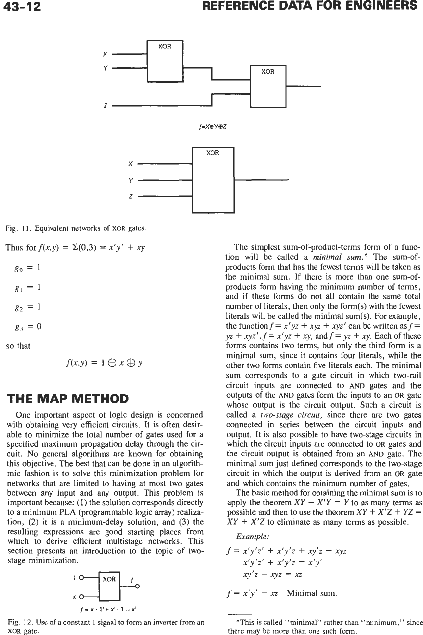
Another very common integrated-circuit gate is the
NOR
gate shown in Fig. 10. It is the dual of the
NAND
gate and is also a single gate that is sufficient to
implement a network for any arbitrary switching func-
tion.
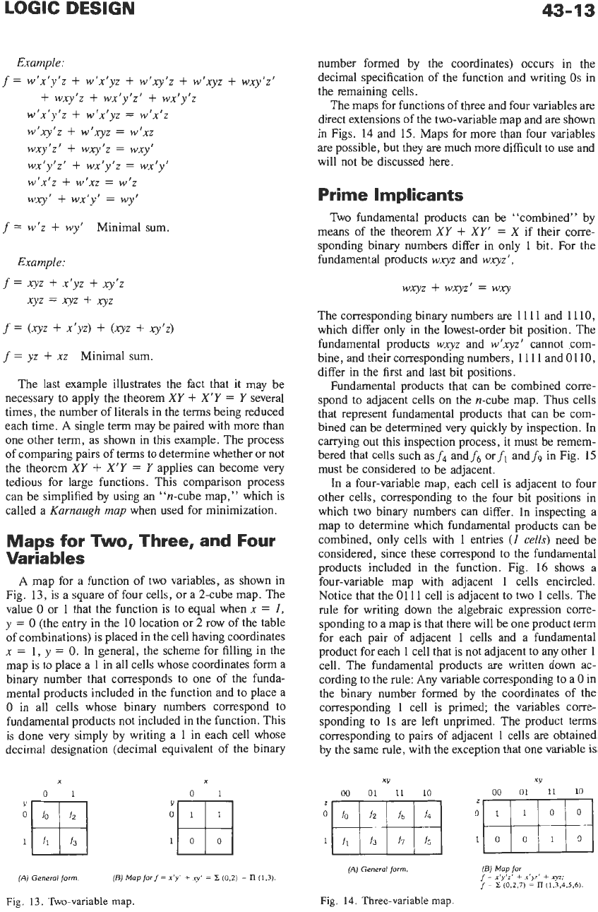
The other important IC gate type is the
sum
modulo
two,
or EXCLUSIVE-OR (XOR) gate,* which has a high
output only when
an
odd number of its inputs are high.
The table
of
combinations for a two-input
XOR
gate is
given in Table
6.
This table shows that the output of an
*The term
XOR
is
used
since
a
two-input gate has
a
1
output
if
one
but
not
both
of
the
inputs
is
equal
to
1.
The OR
gate (sometimes called
INCLUSIVE
OR) has
a
1
output
if
one
or
both
inputs
are
equal
to
1.
TABLE
6.
TABLE
OF
COMBINATIONS
FOR
A
TWO-INPUT
XOR
GATE
(X+
v)'
.=D-
Y
0
(A)
Symbols.
(E)
Table
of
combinations.
Fig.
10.
NOR
gate.
XOR
gate with input xI and x2 is given by
xl
x2
=
x;xz
+
xlx;. It is easily demonstrated that the
XOR
operation
is
commutative and associative; that is,
x
@
y
=
y
@
x
and (x
@
y)
@
z
=
x
@
(y
@
z)
If both inputs of an
XOR
gate are connected together to
x, the output is given by
x
@
x
=
xx'
+
x'x
=
0.
The
fact that this operation is associative means that any
network composed only of
XOR
gates is equivalent to a
single
XOR
gate with all inputs connected directly to it.
This is illustrated in Fig.
11.
Because of the facts that
x
@
x
=
0
and x
@
0
=
x, it is possible to remove any
duplicated inputs
so
that the resulting network contains
only one gate for which no input appears more than
once. Since this gate, called the
reduced
gate,
cannot
function as an inverter, it follows that no network
containing only
XOR
gates can be equivalent to an
inverter. Thus the
XOR
gate is not a complete set by
itself.
The
XOR
gate can perform as an inverter if a signal
representing a constant
1
is
available, since
x
@
1
=
xl'
+
x'l
=
x' (see Fig.
12).
It is still not possible to
construct an
OR
gate by using
XOR
gates and a
1
signal,
for the output of the reduced gate will still be of the
form
X
@
Y
@
1,
which does not equal
1
when either or
both of
X
and
Y
are equal to
1.
A
complete set can be
formed by using both
AND
gates and
XOR
gates. As
demonstrated above, any arbitrary function can be
realized by a network containing only
AND
gates and
inverters. By using
XOR
gates as in Fig.
12
to replace
the inverters, it is possible to obtain a network contain-
ing only
AND
gates and
XOR
gates.
Canonical expressions involving AND, OR, and in-
verter operations have been derived.
It
is
possible to
obtain similar canonical expressions for any complete
set. The canonical expression using
AND
and
XOR
for
two-variable functions
is
where,
f(x,
Y)
=
go
0
gl
'XO
g2
'Y
0
83
'X.Y
go
=fo
gl
=fo
Of2
g2
=
fo
0
fl
83
=
fo
Of1
Of2
Of3
43-12
REFERENCE
DATA
FOR ENGINEERS
Fig. 11.
Equivalent
networks
of
XOR
gates.
Thus for
f(x,y)
=
2(0,3)
=
x’y’
+
xy
so
that
THE
MAP
METHOD
One important aspect of logic design is concerned
with obtaining very efficient circuits. It is often desir-
able to minimize the total number of gates used for a
specified maximum propagation delay through the cir-
cuit.
No
general algorithms are known for obtaining
this objective. The best that can be done in an algorith-
mic fashion is to solve this minimization problem for
networks that are limited to having at most two gates
between any input and any output. This problem is
important because:
(1)
the solution corresponds directly
to a minimum
PLA
(programmable logic array) realiza-
tion,
(2)
it is a minimum-delay solution, and
(3)
the
resulting expressions are good starting places from
which to derive efficient multistage networks. This
section presents an introduction to the topic of two-
stage minimization.
:D
f=x.l’+x‘.I=x’
Fig.
12.
Use
of
a
constant
1
signal
to
form
an
inverter
from
an
XOR
gate.
The simplest sum-of-product-terms form of a func-
tion will be called a
minimal
sum.*
The sum-of-
products form that has the fewest terms will be taken as
the minimal sum. If there is more than one sum-of-
products form having the minimum number of terms,
and if these forms do not all contain the same total
number of literals, then only the form@) with the fewest
literals will be called the minimal sum(s). For example,
the function
f
=
x’yz
+
xyz
+
xyz’
can be written as
f
=
yz
+
xyz‘,
f
=
x’yz
+
xy,
and
f
=
yz
+
xy.
Each of these
forms contains two terms, but only the third form is a
minimal sum, since it contains four literals, while the
other two forms contain five literals each. The minimal
sum corresponds to a gate circuit in which two-rail
circuit inputs are connected to
AND
gates and the
outputs
of
the
AND
gates form the inputs to
an
OR
gate
whose output is the circuit output. Such a circuit is
called a
two-stage
circuit,
since there are two gates
connected in series between the circuit inputs and
output. It is also possible to have two-stage circuits in
which the circuit inputs are connected to
OR
gates and
the circuit output is obtained from an
AND
gate. The
minimal sum just defined corresponds to the two-stage
circuit in which the output is derived from an
OR
gate
and which contains the minimum number of gates.
The basic method for obtaining the minimal sum is
to
apply the theorem
XY
+
X‘Y
=
Y
to as many terms as
possible and then to use the theorem
XY
+
X’Z
+
YZ
=
XY
+
X’Z
to eliminate as many terms as possible.
Example:
f
=
x’y’z‘
+
x’y’z
+
xy’z
+
xyz
xIy’z’
+
x’y’z
=
x’y’
xy’z
+
xyz
=
xz
f
=
x‘y’
+
xz
Minimal sum
*This
is
called
“minimal”
rather
than
“minimum,”
since
there
may
be
more
than
one
such
form.
Example:
f
=
w’x’y’z
+
w’x‘yz
+
w‘xy’z
+
w’xyz
+
wxy’z’
+
wxy’z
+
wx’ylz’
+
wxIy’z
w’x’y’z
+
w‘x’yz
=
W‘X’Z
w’xy‘z
+
w’xyz
=
wlxz
wxy’z’
+
wxy‘z
=
wxyy’
wx’y’z’
+
wx’y‘z
=
wx‘y’
w’x’z
+
w’xz
=
w’z
wxy‘
+
wx’y’
=
wy‘
f
=
w’z
+
wy‘
Minimal sum.
Example:
f
=
xyz
+
x’yz
+
xy’z
f
=
(xyz
+
x’yz)
+
(xyz
+
xy’z)
xyz
=
xyz
+
xyz
f
=
yz
+
xz
Minimal sum.
The last example illustrates the fact that it may be
necessary to apply the theorem
XY
+
X’Y
=
Y
several
times, the number of literals in the terms being reduced
each time.
A
single term may be paired with more than
one other term, as shown in this example. The process
of comparing pairs of terms to determine whether or not
the theorem
XY
+
X‘Y
=
Y
applies can become very
tedious for large functions. This comparison process
can be simplified by using an “n-cube map,” which is
called a
Karnaugh map
when used for minimization.
Maps for
Two,
Three, and Four
Variables
A
map for a function of two variables, as shown in
Fig. 13, is a square of four cells, or a 2-cube map. The
value
0
or 1 that the function is to equal when
x
=
1,
y
=
0
(the entry in the 10 location or
2
row of the table
of combinations) is placed in the cell having coordinates
x
=
1,
y
=
0.
In general, the scheme for filling in the
map is to place a
1
in all cells whose coordinates form a
binary number that corresponds to one of the funda-
mental products included in the function and to place a
0
in all cells whose binary numbers correspond to
fundamental products not included in the function. This
is done very simply by writing a 1 in each cell whose
decimal designation (decimal equivalent of the binary
number formed by the coordinates) occurs in the
decimal specification of the function and writing
Os
in
the remaining cells.
The maps for functions of three and four variables are
direct extensions of the two-variable map and are shown
in Figs.
14
and 15. Maps for more than four variables
are possible, but they are much more difficult to use and
will not be discussed here.
Prime lmplicants
Two fundamental products can be “combined” by
means of the theorem
XY
+
XY’
=
X
if their corre-
sponding binary numbers differ in only
1
bit. For the
fundamental products
wxyz
and
wxyz‘,
wxyz
+
wxyz’
=
wxy
The corresponding binary numbers are
11
11 and 11 10,
which differ only in the lowest-order bit position. The
fundamental products
wxyz
and
w’xyz’
cannot com-
bine, and their corresponding numbers,
1
1 11 and 01
10,
differ in the first and last bit positions.
Fundamental products that can be combined corre-
spond to adjacent cells on the n-cube map. Thus cells
that represent fundamental products that can be com-
bined can be determined very quickly by inspection. In
carrying out this inspection process, it must be remem-
bered that cells such asf4 and
f6
orf, andf9 in Fig. 15
must be considered to be adjacent.
In a four-variable map, each cell is adjacent to four
other cells, corresponding to the four bit positions in
which two binary numbers can differ. In inspecting a
map to determine which fundamental products can be
combined, only cells with
1
entries
(I
cells)
need be
considered, since these correspond to the fundamental
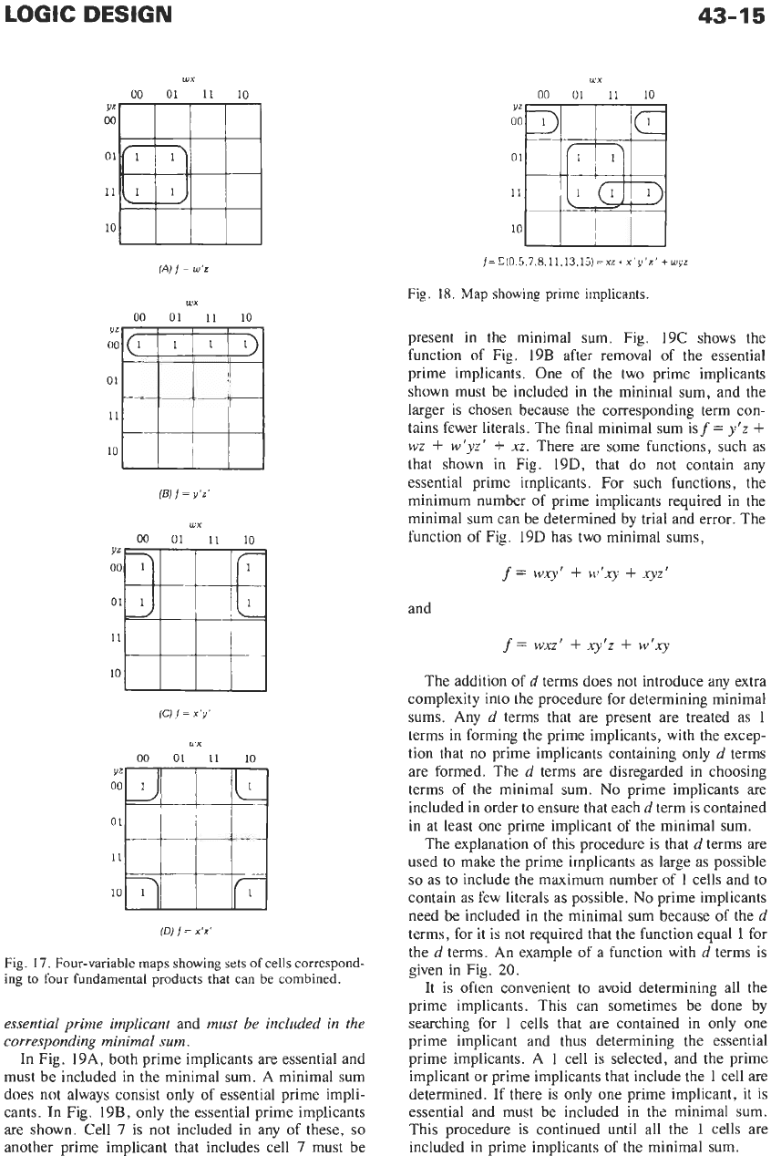
products included in the function. Fig. 16 shows a
four-variable map with adjacent 1 cells encircled.
Notice that the 01 11 cell is adjacent to two 1 cells. The
rule for writing down the algebraic expression corre-
sponding to a map is that there will be one product term
for each pair of adjacent 1 cells and a fundamental
product for each
1
cell that is not adjacent to any other 1
cell. The fundamental products are written down ac-
cording to the rule: Any variable corresponding to a
0
in
the binary number formed by the coordinates of the
corresponding 1 cell is primed; the variables corre-
sponding to 1s are left unprimed. The product terms
corresponding to pairs of adjacent
1
cells are obtained
by the same rule, with the exception that one variable is
XY XY
00
01
11
00
01 11 10
:m]
iml
1
(A)
General
form.
(A)
General
form
(Bj
~~~f~~f=
x’y’
+
rv’
=
z
(0,~)
=
n
(1.3)
Fig.
13.
Two-variable map.
Fig.
14.
Three-variable map.
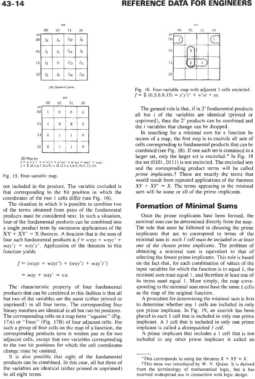
43-14
WX
00 01 11 10
YZ
00
01
11
10
(A)
General
form
WX
00 01 11 10
IW
Map
for
f=
w'x'y'z'
+
w'x'y'r
+
w'qz'
+
w'ry2
+
wq2'
+
W*3L
f-
Z
(0,1,6.7,14.15)
=
Il
(2.3,4,5,8,9,10,11.12,13)
Fig. 15. Four-variable map
not included in the product. The variable excluded is
that corresponding to the bit position in which the
coordinates of the two
1
cells differ (see Fig.
16).
The situation in which it is possible to combine two
of the terms obtained from pairs of the fundamental
products must be considered next.
In
such a situation,
four of the fundamental products can be combined into
a
single product term by successive applications of the
XY
+
XY'
=
X
theorem.
A
function that is the sum of
four such fundamental products
isf=
wxyz
+
wxyz'
+
wxy'z
+
wxy'z'.
Application of the theorem to this
function yields
f=
(wxyz
+
wxyz')
+
(wxy'z
+
wxy'z')
=
wxy
+
wxy'
=
wx
REFERENCE
The characteristic property of four fundamental
products that can be combined in this fashion is that all
but two
of
the variables are the same (either primed
or
unprimed) in all four terms. The corresponding four
binary numbers
are
identical in all but two bit positions.
The corresponding cells
on
a map form "squares" (Fig.
17A)
or "lines" (Fig.
17B)
of four adjacent cells. For
such a group
of
four cells
on
the map
of
a function, the
corresponding products term is written just as for two
adjacent cells, except that two variables corresponding
to the two bit positions for which the cell coordinates
change must be omitted.
It is
also
possible that eight of the fundamental
products can be combined. In this case, all but three
of
the variables are identical (either primed or unprimed)
in
all
eight terms.
DATA
FOR
ENGINEERS
WX
00 01 11 10
:;
md
Fig.
16.
Four-variable map with adjacent
1
cells encircled.
f=
2
(0,5,6,8,15)
=
x'y'z'
+
w'xz
+
xy.
The general rule is that, if in
2'
fundamental products
all but
i of the variables are identical (primed or
unprimed), then the
2'
products can be combined and
the
i
variables that change can be dropped.
In
searching for a minimal sum for a function by
means
of
a map, the first step is to encircle all sets of
cells corresponding to fundamental products that can be
combined (see Fig.
18).
If one such set is contained in a
larger set, only the larger set is encircled.* In Fig.
18
the set (0101,0111) is not encircled. The encircled sets
and the corresponding product terms will be called
prime implicants.
t
These are exactly the terms that
would result from repeated applications of the theorem
XY
+
XY'
=
X.
The terms appearing in the minimal
sum will be some or all of the prime implicants.
Formation
of
Minimal Sums
Once the prime implicants have been formed, the
minimal sum can be determined directly from the map.
The rule that must be followed in choosing the prime
implicants that are to correspond to terms of the
minimal sum is:
each
1
cell must be included in
at
least
one
of
the chosen prime implicants. The problem of
obtaining a minimal sum is equivalent to that of
selecting the fewest prime implicants. This rule
is
based
on
the fact that, for each combination of values of the
input variables for which the function is to equal
1,
the
minimal sum must equal
I,
and therefore at least
one
of
its terms must equal
1.
More simply, the map corre-
sponding to the minimal
sum
must have the same 1 cells
as the map of the original function.
A
procedure for determining the minimal sum is first
to determine whether any
1
cells are included in only
one prime implicant. In Fig.
19,
an asterisk has been
placed in each
1
cell that is included in only one prime
implicant.
A
1
cell that is included
in
only one prime
implicant is called a
distinguished
I
cell.
A
prime implicant that includes a
1
cell that
is
not
included in any other prime implicant is called an
"This corresponds to using the theorem
X
+
XY
=
X.
?This
term
was introduced by
W.
V.
Quine. It
is
derived
from the terminology
of
mathematical logic, but it has
received widespread use in connection with logic design.
LOGIC
DESIGN
WX
u)x
43-15
00 01 11 10
YZ
00
01
11
10
(A)
f
=
w'z
U'X
00 01 11 10
(E)
f
=
y'z'
WX
00
01
11
10
YZ
00
01
11
10
(C)
f
=
x'y'
LUX
00 01 11 10
YZ
00
01
11
10
(D)
f
=
x'z'
Fig.
17.
Four-variable
maps
showing
sets
of
cells
correspond-
ing
to
four fundamental products
that
can be combined.
essential prime implicant
and
must be included
in
the
corresponding minimal
sum.
In
Fig. 19A, both prime implicants are essential and
must be included in the minimal sum. A minimal sum
does not always consist only of essential prime impli-
cants.
In
Fig. 19B, only the essential prime implicants
are shown. Cell
7
is not included in any of these, so
another prime implicant that includes cell
7
must be
00 01 11 10
YZ
00
01
11
10
,f=
q0.5.7.8.11.13.15)
=xz+x'y'z'
+
wyz
Fig. 18.
Map
showing prime implicants.
present in the minimal sum. Fig. 19C shows the
function of Fig. 19B after removal of the essential
prime implicants. One of the two prime implicants
shown must be included in the minimal sum, and the
larger is chosen because the corresponding term con-
tains fewer literals. The final minimal sum isf=
y'z
+
wz
+
w'yz'
+
xz.
There are some functions, such as
that shown in Fig. 19D, that do not contain any
essential prime implicants. For such functions, the
minimum number of prime implicants required in the
minimal sum can be determined by trial and error. The
function of Fig. 19D has two minimal sums,
f
=
wxy'
+
Wlxy
+
xyz'
and
f
=
wxz'
+
xy'z
+
w'xy
The addition of
d
terms does not introduce any extra
complexity into the procedure for determining minimal
sums. Any
d
terms that are present are treated as 1
terms in forming the prime implicants, with the excep-
tion that
no
prime implicants containing only
d
terms
are formed. The
d
terms are disregarded in choosing
terms of the minimal sum.
No
prime implicants are
included in order to ensure that each
d
term is contained
in at least one prime implicant of the minimal sum.
The explanation of this procedure is that
d
terms are
used to make the prime implicants as large as possible
so
as to include the maximum number of 1 cells and
to
contain as few literals as possible.
No
prime implicants
need be included in the minimal sum because
of
the
d
terms, for it is not required that the function equal 1 for
the
d
terms. An example of a function with
d
terms is
given in Fig.
20.
It is often convenient to avoid determining all the
prime implicants. This can sometimes be done by
searching for 1 cells that are contained in only one
prime implicant and thus determining the essential
prime implicants. A 1 cell is selected, and the prime
implicant or prime implicants that include the 1 cell are
determined. If there is only one prime implicant, it is
essential and must be included in the minimal sum.
This procedure is continued until all the 1 cells are
included in prime implicants of the minimal sum.