Severns Rudy. Design of snubbers for power circuits
Подождите немного. Документ загружается.


11
Figure 7

12
Usually C
test
is approximately equal to twice the switch capacitance
An alternate method for determining Lp in higher power circuits is to take advantage of the
voltage step (V
step
) which appears in V
ce
or V
ds
due to the dI/dt of the current flowing in Lp at turn-on:
At switch turn-on C
s
will be charged. This means that there will be a current spike in the switch due to
the discharge of C
s
through R
s
in addition to the normal current flow. This is a short transient pulse
which rapidly decays but it can add substantially to the turn-on current and should be taken into account.
It should be noted that the RCD snubber discussed in the next section will also have this turn-on current
spike but that spike can be controlled more easily because the value for R
s
does not have to be optimized
for maximum damping.
RC snubbers are very useful for low and medium power applications but when the power level is
more than a few hundred watts the loss in the snubber can be excessive and other types of snubbers need
to be considered. The RC snubber does have a place in high power applications as a secondary damping
network to suppress high frequency ringing which does not have a lot of energy associated with it.
RCD snubber design
The RCD snubber as shown in figure 8 has several advantages over the RC snubber:
· In addition to peak voltage limiting, the circuit can reduce the total circuit loss, including
both switching and snubber losses.
· Much better load lines can be achieved, allowing the load line to pass well within the SOA.
· For a given value of C
s
, the total losses will be less
· The shunt capacitance across the switch (Cp) is a useful part of the snubber
There is one disadvantage however. Because of the diode across R
s
, the effective value for R
s
,
during the charging of C
s
, is essentially zero. This is not the optimum value and, for a given C
s
, E
1
will
be higher than it would be in an optimized RC snubber.
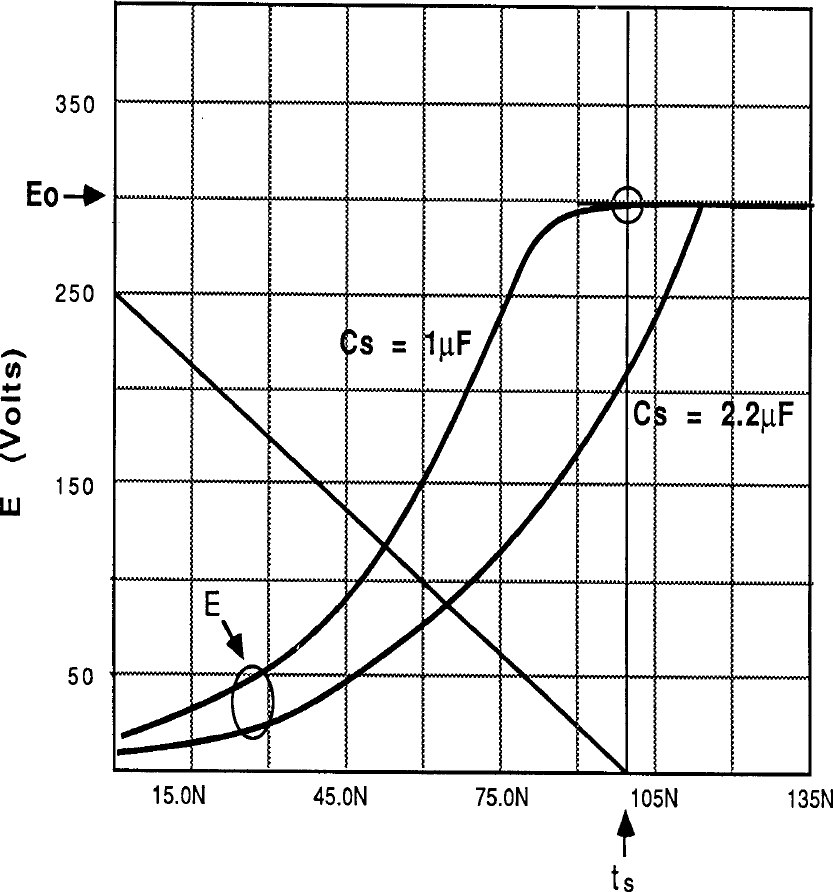
Typical turn-off waveforms for this snubber are given in figure 9. These waveforms assume that
Lp = 0. The effect of Lp will be considered shortly. The key feature of these waveforms is that the switch
voltage rises slowly as the switch current falls. This means that the high peak power associated with

13
Figure 8
14
Figure 9
I

15
simultaneous maximum voltage and current is eliminated. The net result is much lower peak stress and
switching loss. Voltage waveforms for two different values of C
s
are shown. In this example I
o
= 10 A
and E
o
= 300 V. As C
s
is made larger the peak power and the switching loss will be lower. However,
larger C
s
means greater loss in R
s
when the switch turns on and C
s
is discharged through R
s
and the
switch. Again we see the tradeoff between snubber efficacy and loss.
Depending on the size of C
s
the switch voltage may reach E
o
before, at the same time, or after the
switch current reaches zero. The case where E = E
o
at the instant that I = 0 is defined as a “normal”
snubber and C
s
= C
[2]
n
, where :
Where t
s
is the fall time of the switch current (see figure 9). For the example given in figure 9, C
n
=
1.667 nF.
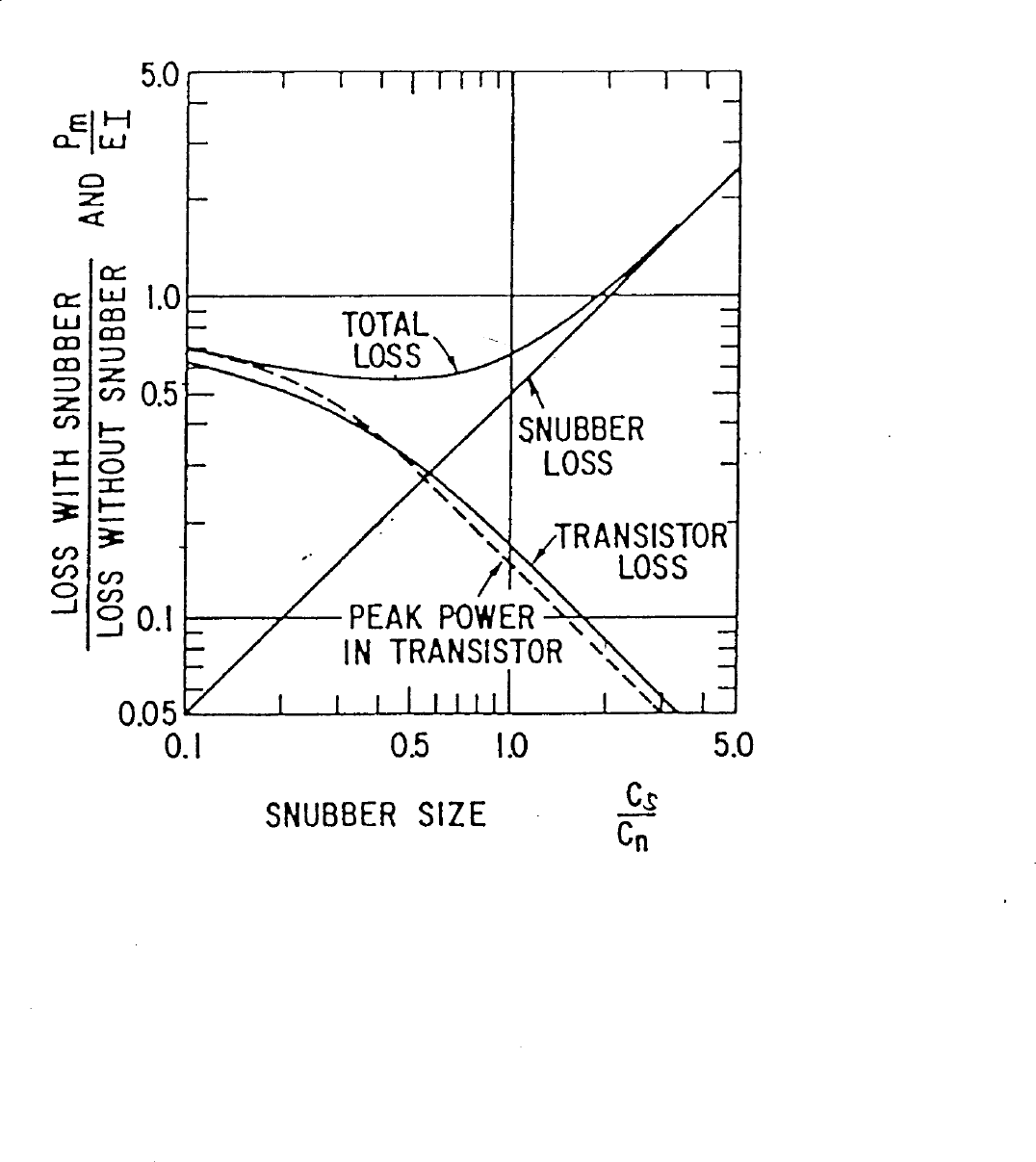
The relationships between C
n
, switching loss, peak switch stress, snubber loss and total loss are
shown in figure 10. Snubber size is shown relative to C
n
. When even a small snubber is used (C
s
< C
n
) the
switching loss drops quickly. As C
s
is made larger however, the improvement in switch loss decreases.
For example, for C
s
= C
n
, the switch loss is down to 16%. Making C
s
larger will reduce the switching
loss only a small amount but will increase the snubber loss substantially. There is in fact a broad mini-
mum loss around C
s
= 0.45 C
n
, where the total loss is reduced to 53% of what it would have been
without the snubber. It is important to remember that C
p
is part of C
s
and that the actual value for C
s
=
.45 C
n
- C
p
. For C
s
/C
n
= 2 the total loss is equal to what it would have been if no snubber were used,
however the switching load line will have very low stress.
In those cases where the primary concern is to reduce the total switching loss, the value for C
s
is usually set to .5 Cn. In this case R
s
is selected to allow the voltage on C
s
to decay to a small value
during the minimum switch on time (t
on,min
). The capacitor voltage decay is a simple RC exponential
and in two time constants (τ = R
s
C
s
) will be down to 0.14 E
o
. This is usually sufficient. The value of
R
s
is then:
When L
p
is significant there will be voltage overshoot during turn-off. If E
1
must be controlled then
different values for C
s
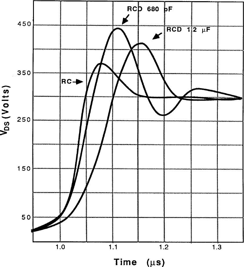
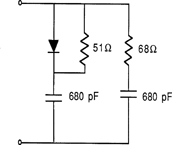
may be necessary and a compromise made. Figure 11 gives a comparison be-
tween the RC snubber developed earlier and an RCD snubber using the same component values (R
s
=
51W and C
s
= 680 pF). Note that the loss will be lower but the peak voltage is higher for the RCD
snubber. This is typical. For similar total loss, C
s
can be larger in the RCD snubber which will reduce E
1
.
Increasing C
s
to 1.2 nF reduces E
1
to 424 V. C
s
could be increased further but for the same total loss, E
1
will still be higher in the RCD snubber.
Combined snubber: When it is important to minimize both the loss in the switch and E
1
16
Figure 10
17
Figure 11

18
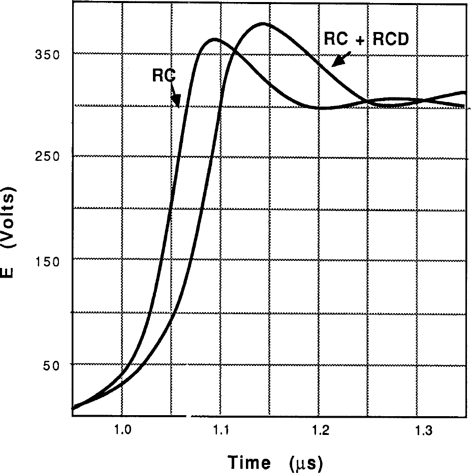
a combination snubber, using both RC and RCD, can produce very good results with low losses. An
example of such a combination is given in figure 12 and the resulting waveform is compared to the
previous RC snubber, using the same circuit conditions, in figure 13.
Component selection and layout
The components in snubbers can be very highly stressed and must therefore be selected with
some care.
Layout and inductance
One of the primary reasons for using snubbers is the presence of parasitic inductances (L
p
) in the
circuit which generate voltage spikes and ringing when excited by the switching action. Larger parasitic
inductance means larger snubber components and more dissipation. Before actually designing the snub-
ber, it is important to minimize the circuit parasitic inductances and careful circuit layout is the key. As
power levels rise this becomes progressively more important because of the increasing dI/dt.
Figure 14A illustrates a typical inverter pole or converter half-bridge. The bus which connects
the source (V
dc
) to the “+” and “-” ends of the pole will have some inherent inductance, both in the bus
structure and in the energy storage capacitors (C
1
, ESL). The effect of L
p
can be greatly reduced by
placing smaller, low ESL, capacitors as close as possible to the switches as shown by C
2
. One possibility
is to use CDE snubber capacitor modules which connect directly to the IGBT module as shown in figure
15. These modules are available as either a simple capacitor or they may include one or more snubber
diodes to implement an RCD snubber.
In some cases the addition of C
2
by itself may not be a complete answer because the bus voltage
may ring due to the resonance of Lp, C
1
and C
2
. An alternative is to use an RCD snubber as a clamp as
shown in figure 14B. The average voltage across C
2
will be equal to the bus voltage. At turn-off the
voltage across C
2
will rise as it limits the peak switch voltage but later in the cycle the voltage is reset to
the bus voltage through R
s
. R
s
also damps the bus voltage ringing. An additional advantage of this
approach is that L
p
acts as a turn-on snubber, reducing turn-on switching loss.
Because of the very large dI/dt’s which are common in snubbers, small amounts of parasitic
inductance within the snubber can interfere with snubber action leading to higher than expected peak
voltages. Parasitic inductance comes from two sources: intrinsic to the components due to physical size
and lead configuration and from the layout. Component inductance can be minimized by the choice of
package (radial versus axial for example) and can be further reduced by using several smaller devices in
parallel. Paralleling is particularly useful in high power snubbers because in addition to allowing lower
inductance configurations, it can improve the surface area-volume ratio allowing better cooling and
higher rms currents.
The primary source of layout inductance is the connection from the snubber components to the
switch. The snubber components should be placed as close as possible to the switch terminals. The
components should be arranged so that the current
19
Figure 12
20
Figure 13