Справочник по мощным TMOS транзисторам (MOTOROLA)
Подождите немного. Документ загружается.

4–198
Motorola TMOS Power MOSFET Transistor Device Data
R
DS(on)
, DRAIN–TO–SOURCE RESISTANCE (OHMS)R
DS(on)
, DRAIN–TO–SOURCE RESISTANCE (OHMS)
R
DS(on)
, D
R
A
I
N
–T
O
–
SO
UR
C
E
RE
S
I
S
T
ANC
E
(
O
H
MS
)
1
0
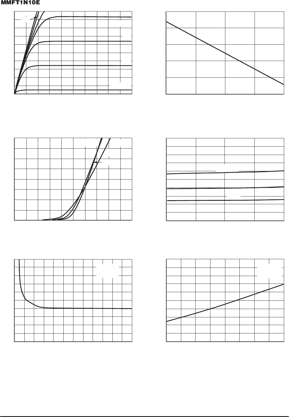
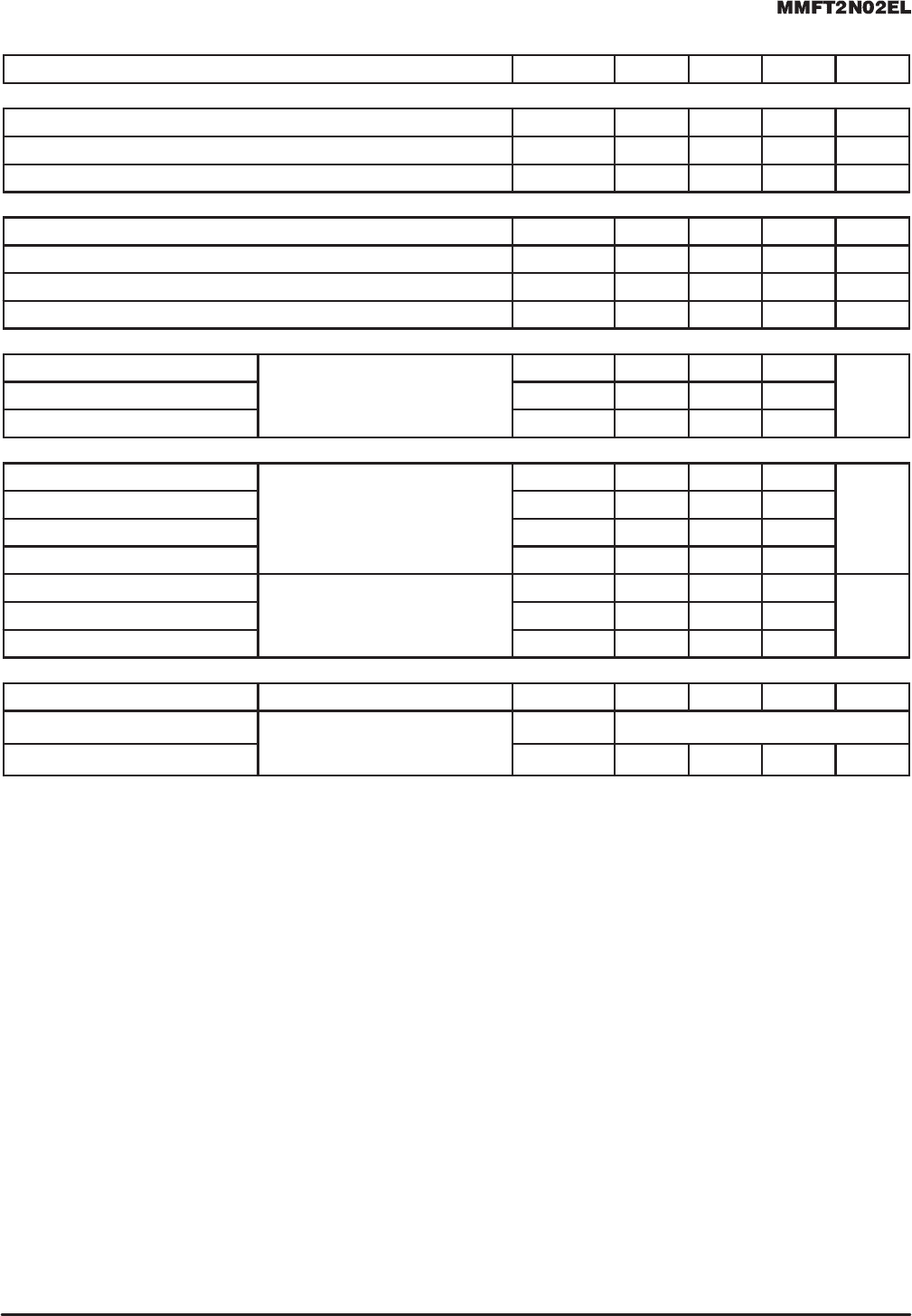
Figure 1. On Region Characteristics
V
DS
, DRAIN–TO–SOURCE VOLTAGE (VOLTS)
T
J
= 25°C
Figure 2. Gate–Threshold Voltage Variation
With Temperature
T
J
, JUNCTION TEMP (°C)
Figure 3. Transfer Characteristics
V
GS
, GATE–TO–SOURCE VOLTAGE (VOLTS)
Figure 4. On–Resistance versus Drain Current
I
D
, DRAIN CURRENT (AMPS)
Figure 5. On–Resistance versus
Gate–to–Source Voltage
V
GS
, GATE–TO–SOURCE VOLTAGE (VOLTS)
Figure 6. On–Resistance versus Junction
Temperature
T
J
, JUNCTION TEMPERATURE (°C)
V
DS
= V
GS
I
D
= 1.0 mA
I
D
, D
R
A
I
N C
URRE
N
T
(
AMPS
)
8
6
4
2
0
1086420
V
GS(TH)
, GATE THRESHOLD VOLTAGE
(NORMALIZED)
1.1
–50
1.0
0.9
0.8
0.7
0 50 100 150
4
I
D
, D
R
A
I
N C
URRE
N
T
(
AMPS
)
3
2
1
0
1086420
0.5
0
0.3
0.2
0.1
0
24
0.4
0.5
0.4
0.3
0.1
0
161210864
0.5
–50
0.3
0.2
0.1
0
0 50 100 150
0.4
0.2
14
7 V
6 V
V
GS
= 4 V
5 V
9 V
8 V
V
DS
= 10 V
100°C
T
J
= –55°C
25°C
T
J
= 100°C
25°C
–55°C
T
J
= 25°C
I
D
= 1 A
V
GS
= 10 V
I
D
= 1 A
10 V
V
GS
= 10 V
1
.
2
4–199
Motorola TMOS Power MOSFET Transistor Device Data
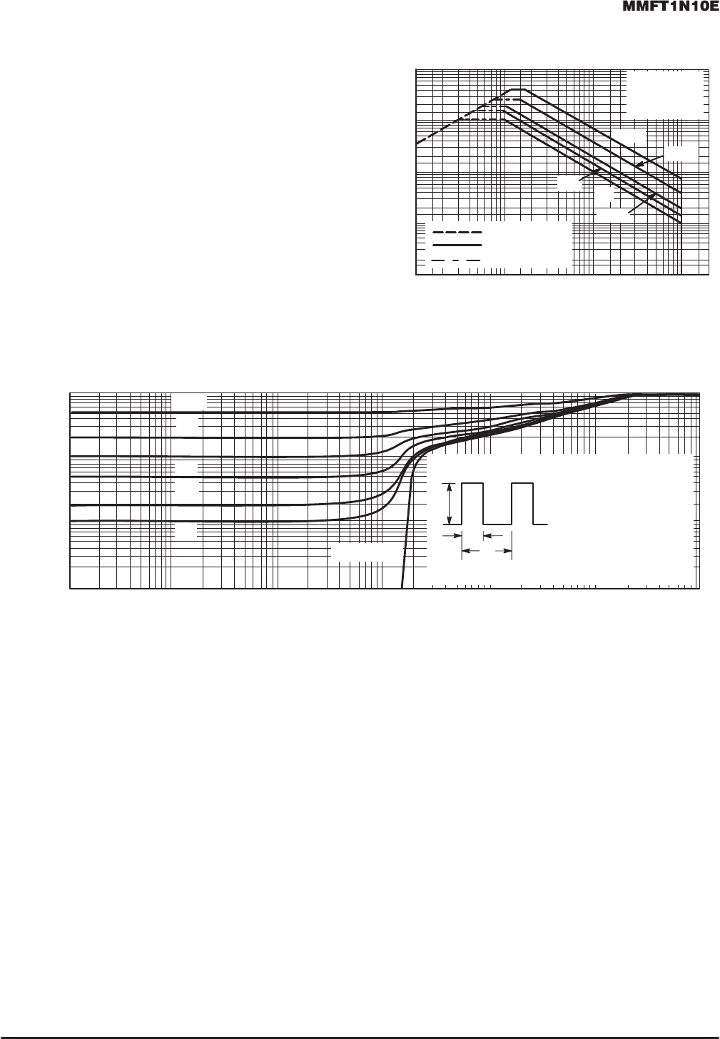
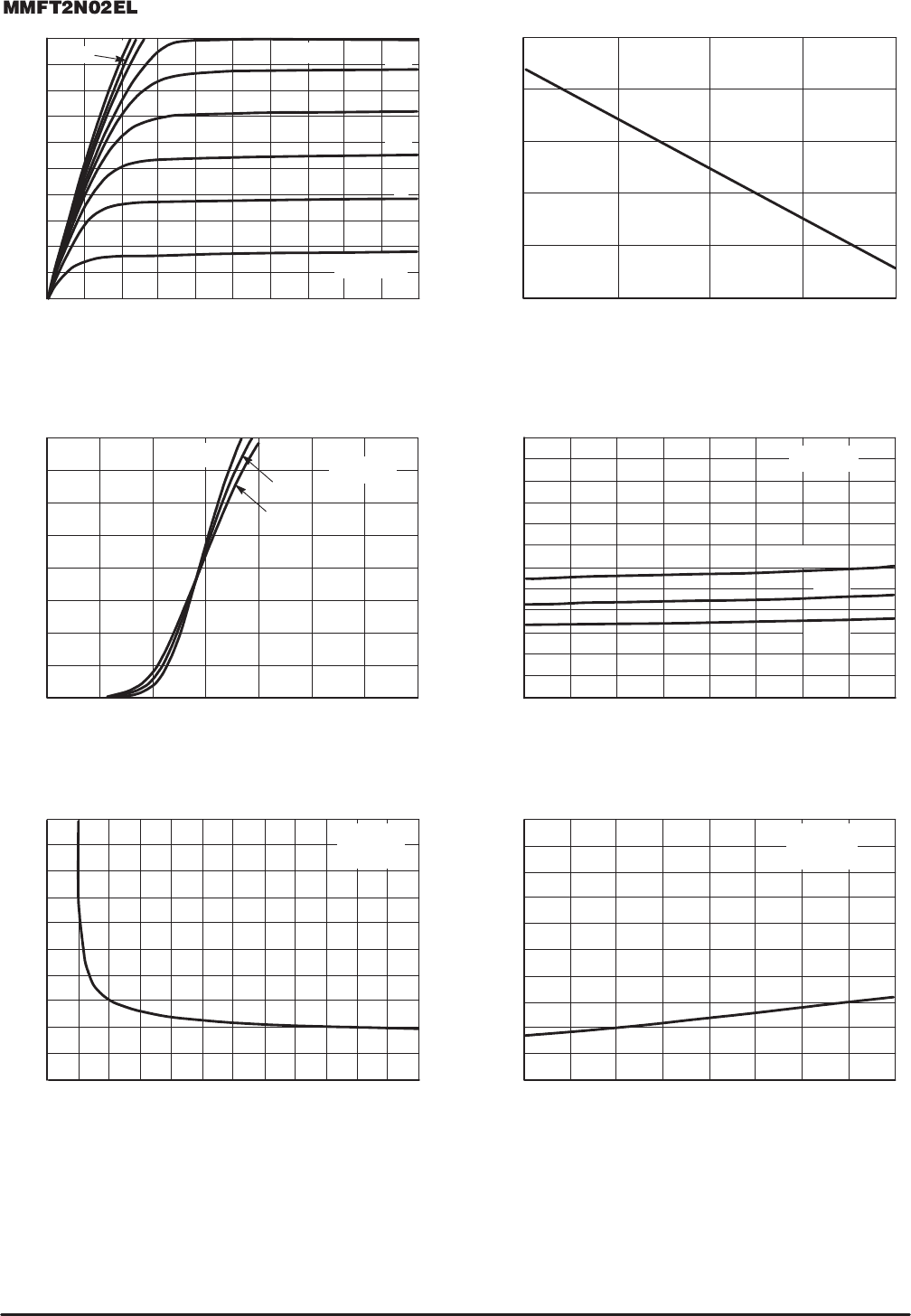
FORWARD BIASED SAFE OPERATING AREA
The FBSOA curves define the maximum drain–to–source
voltage and drain current that a device can safely handle
when it is forward biased, or when it is on, or being turned on.
Because these curves include the limitations of simultaneous
high voltage and high current, up to the rating of the device,
they are especially useful to designers of linear systems. The
curves are based on an ambient temperature of 25
°C and a
maximum junction temperature of 150
°C. Limitations for re-
petitive pulses at various ambient temperatures can be de-
termined by using the thermal response curves. Motorola
Application Note, AN569, “Transient Thermal Resistance–
General Data and Its Use” provides detailed instructions.
SWITCHING SAFE OPERATING AREA
The switching safe operating area (SOA) is the boundary
that the load line may traverse without incurring damage to
the MOSFET. The fundamental limits are the peak current,
I
DM
and the breakdown voltage, BV
DSS
. The switching SOA
is applicable for both turn–on and turn–off of the devices for
switching times less than one microsecond.
Figure 7. Maximum Rated Forward Biased
Safe Operating Area
V
GS
= 20 V
SINGLE PULSE
T
A
= 25°C
10
I
D
, DRAIN CURRENT (AMPS)
0.1
1
0.1
0.01
0.001
1 10 100
V
DS
, DRAIN–TO–SOURCE VOLTAGE (VOLTS)
DC
20 ms
1 s
500 ms
100 ms
R
DS(on)
LIMIT
THERMAL LIMIT
PACKAGE LIMIT
Figure 8. Thermal Response
1.0
0.1
0.001
1.0E–05 1.0E–04 1.0E–03 1.0E–02 1.0E–01 1.0E+00
r(t), EFFECTIVE THERMAL RESISTANCE
t, TIME (s)
0.1
0.01
0.2
0.02
0.01
D = 0.5
SINGLE PULSE
(NORMALIZED)
0.05
R
θJA
(t) = r(t) R
θJA
R
θJA
= 156°C/W MAX
D CURVES APPLY FOR POWER
PULSE TRAIN SHOWN
READ TIME AT t
1
T
J(pk)
– T
A
= P
(pk)
R
θJA
(t)
P
(pk)
t
1
t
2
DUTY CYCLE, D = t
1
/t
2
1.0E+01
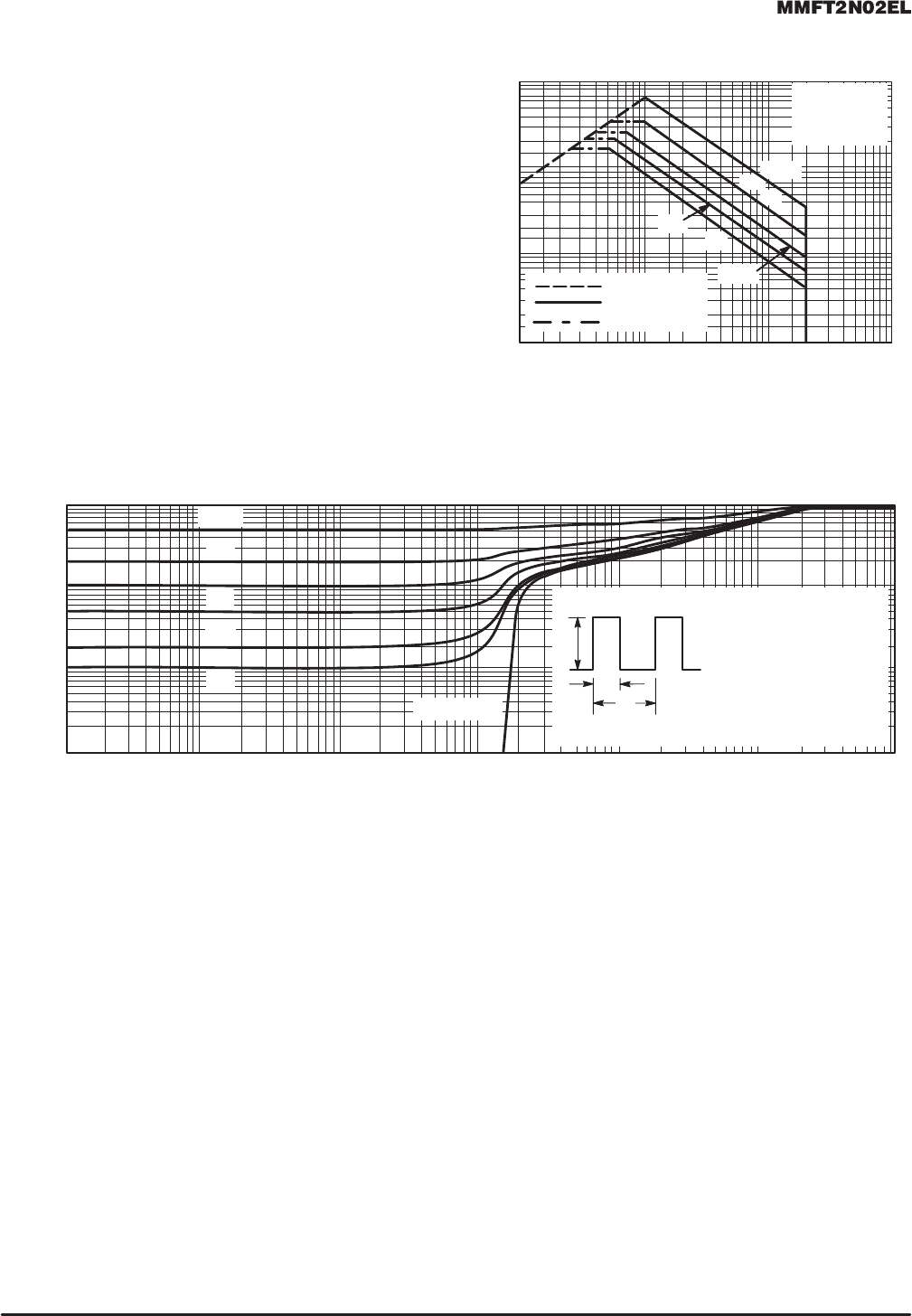
COMMUTATING SAFE OPERATING AREA (CSOA)
The Commutating Safe Operating Area (CSOA) of Figure 10 defines the limits of safe operation for commutated source–drain
current versus re–applied drain voltage when the source–drain diode has undergone forward bias. The curve shows the limita-
tions of I
FM
and peak V
DS
for a given rate of change of source current. It is applicable when waveforms similar to those of Figure
9 are present. Full or half–bridge PWM DC motor controllers are common applications requiring CSOA data.
Device stresses increase with increasing rate of change of source current so dI
S
/dt is specified with a maximum value. Higher
values of dI
S
/dt require an appropriate derating of I
FM
, peak V
DS
or both. Ultimately dI
S
/dt is limited primarily by device, package,
and circuit impedances. Maximum device stress occurs during t
rr
as the diode goes from conduction to reverse blocking.
V
DS(pk)
is the peak drain–to–source voltage that the device must sustain during commutation; I
FM
is the maximum forward
source–drain diode current just prior to the onset of commutation.
V
R
is specified at 80% rated BV
DSS
to ensure that the CSOA stress is maximized as I
S
decays from I
RM
to zero.
R
GS
should be minimized during commutation. T
J
has only a second order effect on CSOA.
Stray inductances in Motorola’s test circuit are assumed to be practical minimums. dV
DS
/dt in excess of 10 V/ns was at-
tained with dI
S
/dt of 400 A/µs.

4–200
Motorola TMOS Power MOSFET Transistor Device Data
R
G
t
V
DS
L
I
L
V
DD
Figure 9. Commutating Waveforms
t
P
BV
DSS
V
DD
I
L(t)
t, (TIME)
Figure 10. Commutating Safe Operating Area
(CSOA)
15 V
V
GS
0
90%
I
FM
dl
S
/dt
I
S
10%
t
rr
t
frr
0.25 I
RM
I
RM
t
on
V
DS
V
f
V
dsL
V
R
V
DS(pk)
MAX. CSOA
STRESS AREA
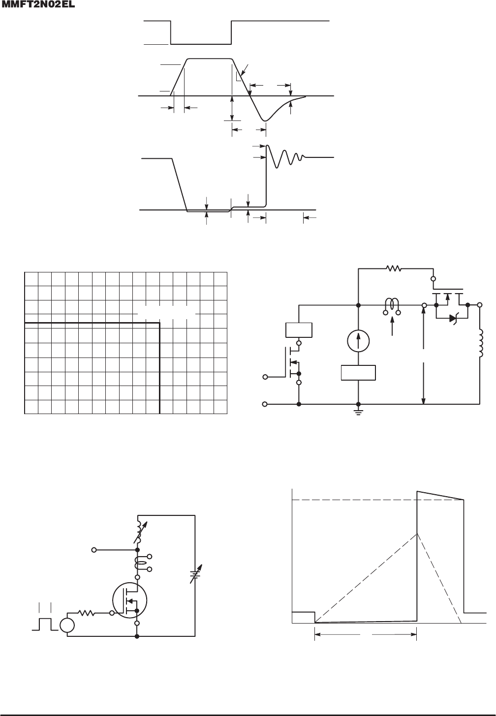
Figure 11. Commutating Safe Operating Area
Test Circuit
Figure 12. Unclamped Inductive Switching
Test Circuit
V
DS
, DRAIN–TO–SOURCE VOLTAGE (VOLTS)
+
–
+
–
Figure 13. Unclamped Inductive Switching
Waveforms
V
R
V
GS
I
FM
20 V
R
GS
DUT
I
S
V
DS
L
i
V
R
= 80% OF RATED V
DSS
V
dsL
= V
f
+ L
i
⋅ dl
S
/dt
I
S
, SOURCE CURRENT (AMPS)
5
0
4.5
4
3.5
3
2.5
2
1.5
0
20 40 60 80 100 120 140
1
0.5
dI
S
/dt ≤ 400 A/µs
4–201
Motorola TMOS Power MOSFET Transistor Device Data
Figure 14. Capacitance Variation With Voltage
SAME
DEVICE TYPE
AS DUT
V
in
+18 V V
DD
10 V
100 k
0.1 µF
FERRITE
BEAD
DUT
100
2N3904
2N3904
47 k
15 V
100 k
V
in
= 15 V
pk
; PULSE WIDTH ≤ 100 µs, DUTY CYCLE ≤ 10%.
1mA
47 k
Figure 15. Gate Charge versus Gate–To–Source Voltage
GATE–TO–SOURCE OR DRAIN–TO–SOURCE VOLTAGE (VOLTS)
C, CAPACITANCE (pF)
C
rss
C
iss
C
oss
1400
20
1200
1000
800
600
400
200
0
15 10 5 0 5 10 15 20
V
GS
V
DS
Figure 16. Gate Charge Test Circuit
Q
g
, TOTAL GATE CHARGE (nC)
8
0
6
4
2
0
2468
V
GS
, GATE–TO–SOURCE VOLTAGE (VOLTS)
C
iss
C
rss
T
J
= 25°C
f = 1 MHz
10
T
J
= 25°C
I
D
= 1 A
V
GS
= 10 V
V
DS
= 50 V V
DS
= 80 V
C
oss
4–202
Motorola TMOS Power MOSFET Transistor Device Data
N–Channel Enhancement Mode
Silicon Gate TMOS E–FET
SOT–223 for Surface Mount
This advanced E–FET is a TMOS Medium Power MOSFET
designed to withstand high energy in the avalanche and commuta-
tion modes. This device is also designed with a low threshold
voltage so it is fully enhanced with 5 Volts. This new energy efficient
device also offers a drain–to–source diode with a fast recovery
time. Designed for low voltage, high speed switching applications in
power supplies, dc–dc converters and PWM motor controls, these
devices are particularly well suited for bridge circuits where diode
speed and commutating safe operating areas are critical and offer
additional safety margin against unexpected voltage transients.
The device is housed in the SOT–223 package which is designed
for medium power surface mount applications.
• Silicon Gate for Fast Switching Speeds
• Low Drive Requirement to Interface Power Loads to Logic
Level ICs, V
GS(th)
= 2 Volts Max
• Low R
DS(on)
— 0.15 Ω max
• The SOT–223 Package can be Soldered Using Wave or Re-
flow. The Formed Leads Absorb Thermal Stress During Sol-
dering, Eliminating the Possibility of Damage to the Die
• Available in 12 mm Tape and Reel
Use MMFT2N02ELT1 to order the 7 inch/1000 unit reel.
Use MMFT2N02ELT3 to order the 13 inch/4000 unit reel.
MAXIMUM RATINGS
(T
A
= 25°C unless otherwise noted)
Rating
Symbol Value Unit
Drain–to–Source Voltage V
DS
20
Vdc
Gate–to–Source Voltage — Continuous V
GS
±15
Vdc
Drain Current — Continuous
Drain Current — Pulsed
I
D
I
DM
1.6
6.4
Adc
Total Power Dissipation @ T
A
= 25°C
Derate above 25°C
P
D
(1)
0.8
6.4
Watts
mW/°C
Operating and Storage Temperature Range T
J
, T
stg
–65 to 150 °C
Single Pulse Drain–to–Source Avalanche Energy — Starting T
J
= 25°C
(V
DD
= 10 V, V
GS
= 5 V, Peak I
L
= 2 A, L = 0.2 mH, R
G
= 25 Ω)
E
AS
66 mJ
DEVICE MARKING
2N02L
THERMAL CHARACTERISTICS
Thermal Resistance — Junction–to–Ambient (surface mounted) R
θJA
156 °C/W
Maximum Temperature for Soldering Purposes,
Time in Solder Bath
T
L
260
10
°C
Sec
(1) Power rating when mounted on FR–4 glass epoxy printed circuit board using recommended footprint.
Preferred devices are Motorola recommended choices for future use and best overall value.
REV 3
SEMICONDUCTOR TECHNICAL DATA
MEDIUM POWER
LOGIC LEVEL TMOS FET
1.6 AMP
20 VOLTS
R
DS(on)
= 0.15 OHM
Motorola Preferred Device
CASE 318E–04, STYLE 3
TO–261AA
D
S
G
2,4
3
1
1
2
3
4
4–203
Motorola TMOS Power MOSFET Transistor Device Data
ELECTRICAL CHARACTERISTICS (T
A
= 25°C unless otherwise noted)
Characteristic Symbol Min Typ Max Unit
OFF CHARACTERISTICS
Drain–to–Source Breakdown Voltage, (V
GS
= 0, I
D
= 250 µA) V
(BR)DSS
20 — — Vdc
Zero Gate Voltage Drain Current, (V
DS
= 20 V, V
GS
= 0) I
DSS
— — 10 µAdc
Gate–Body Leakage Current, (V
GS
= 15 V, V
DS
= 0) I
GSS
— — 100 nAdc
ON CHARACTERISTICS
Gate Threshold Voltage, (V
DS
= V
GS
, I
D
= 1 mA) V
GS(th)
1 — 2 Vdc
Static Drain–to–Source On–Resistance, (V
GS
= 5 V, I
D
= 0.8 A) R
DS(on)
— — 0.15 Ohms
Drain–to–Source On–Voltage, (V
GS
= 5 V, I
D
= 1.6 A) V
DS(on)
— — 0.32 Vdc
Forward Transconductance, (V
DS
= 10 V, I
D
= 0.8 A) g
FS
— 2.6 — mhos
DYNAMIC CHARACTERISTICS
Input Capacitance
(V
DS
=
15 V,
C
iss
— 580 —
Output Capacitance
(V
DS
=
15
V
,
V
GS
= 0,
f 1 MH )
C
oss
— 430 —
pF
Reverse Transfer Capacitance
f
= 1
MH
z
)
C
rss
— 250 —
SWITCHING CHARACTERISTICS
Turn–On Delay Time t
d(on)
— 16 —
Rise Time
(V
DD
= 15 V, I
D
= 1.6 A
V
GS
=5VR
G
= 50 ohms
t
r
— 73 —
ns
Turn–Off Delay Time
V
GS
=
5
V
,
R
G
=
50
ohms
,
R
GS
= 25 ohms)
t
d(off)
— 77 —
ns
Fall Time
GS
t
f
— 107 —
Total Gate Charge
(V
DS
=
16 V, I
D
=
1.6 A,
Q
g
— 20 —
Gate–Source Charge
(V
DS
=
16
V
,
I
D
=
1
.
6
A
,
V
GS
= 5 Vdc)
SFi 15d16
Q
gs
— 1.7 —
nC
Gate–Drain Charge
S
ee
Fi
gures 15 an
d
16
Q
gd
— 6 —
SOURCE DRAIN DIODE CHARACTERISTICS
(1)
Forward On–Voltage I
S
= 1.6 A, V
GS
= 0 V
SD
— 0.9 — Vdc
Forward Turn–On Time
I
S
= 1.6 A, V
GS
= 0,
dl
S
/dt = 400 A/µs
t
on
Limited by stray inductance
Reverse Recovery Time
dl
S
/dt
=
400
A/µs
,
V
R
= 16 V
t
rr
— 55 —
ns
(1) Pulse Test: Pulse Width ≤ 300 µs, Duty Cycle ≤ 2%
4–204
Motorola TMOS Power MOSFET Transistor Device Data
R
DS(on)
, DRAIN–TO–SOURCE RESISTANCE (OHMS)R
DS(on)
, DRAIN–TO–SOURCE RESISTANCE (OHMS)
R
DS(on)
, D
R
A
I
N
–T
O
–
SO
UR
C
E
RE
S
I
S
T
ANC
E
(
O
H
MS
)
1
0
Figure 1. On Region Characteristics
V
DS
, DRAIN–TO–SOURCE VOLTAGE (VOLTS)
T
J
= 25°C
10
Figure 2. Gate–Threshold Voltage Variation
With Temperature
T
J
, JUNCTION TEMP (°C)
Figure 3. Transfer Characteristics
V
GS
, GATE–TO–SOURCE VOLTAGE (VOLTS)
Figure 4. On–Resistance versus Drain Current
I
D
, DRAIN CURRENT (AMPS)
Figure 5. On–Resistance versus
Gate–to–Source Voltage
V
GS
, GATE–TO–SOURCE VOLTAGE (VOLTS)
Figure 6. On–Resistance versus Junction
Temperature
T
J
, JUNCTION TEMPERATURE (°C)
V
DS
= V
GS
I
D
= 1 mA
I
D
, D
R
A
I
N C
URRE
N
T
(
AMPS
)
8
6
4
2
0
543210
V
GS(TH)
, GATE THRESHOLD VOLTAGE
(NORMALIZED)
1.1
–50
1
0.9
0.8
0.7
0 50 100 150
V
DS
= 8 V
I
D
, D
R
A
I
N C
URRE
N
T
(
AMPS
)
8
6
2
0
76420
0.3
0
0.2
0.15
0.1
0
1234
T
J
= –55°C
100°C
25°C
0.25
–55°C
0.5
0.4
0.3
0.1
0
865432
0.3
–50
0.1
0
0 50 100 150
0.4
0.2
7
4
0.05
0.5
0.2
7
6
5
4.5
4
3.5
3
T
J
= 100°C
25°C
T
J
= 25°C
I
D
= 1.6 A
V
GS
= 5 V
I
D
= 1.6 A
V
GS
= 5 V
1
.
2
V
GS
= 2.5 V
4–205
Motorola TMOS Power MOSFET Transistor Device Data
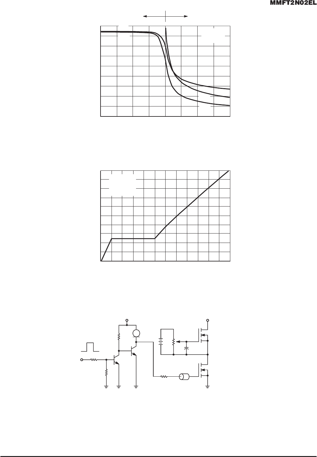
FORWARD BIASED SAFE OPERATING AREA
The FBSOA curves define the maximum drain–to–source
voltage and drain current that a device can safely handle
when it is forward biased, or when it is on, or being turned on.
Because these curves include the limitations of simultaneous
high voltage and high current, up to the rating of the device,
they are especially useful to designers of linear systems. The
curves are based on an ambient temperature of 25
°C and a
maximum junction temperature of 150
°C. Limitations for re-
petitive pulses at various ambient temperatures can be de-
termined by using the thermal response curves. Motorola
Application Note, AN569, “Transient Thermal Resistance–
General Data and Its Use” provides detailed instructions.
SWITCHING SAFE OPERATING AREA
The switching safe operating area (SOA) is the boundary
that the load line may traverse without incurring damage to
the MOSFET. The fundamental limits are the peak current,
I
DM
and the breakdown voltage, BV
DSS
. The switching SOA is
applicable for both turn–on and turn–off of the devices for
switching times less than one microsecond.
Figure 7. Maximum Rated Forward Biased
Safe Operating Area
V
GS
= 15 V
SINGLE PULSE
T
A
= 25°C
1 s
20 ms
DC
10
I
D
, D
R
A
I
N C
URRE
N
T
(
AMPS
)
0.1
1
0.1
0.01
1 10 100
V
DS
, DRAIN–TO–SOURCE VOLTAGE (VOLTS)
100
ms
500 ms
R
DS(on)
LIMIT
THERMAL LIMIT
PACKAGE LIMIT
1.0
0.1
0.001
1.0E–05 1.0E–04 1.0E–03 1.0E–02 1.0E–01 1.0E+00
r(t), EFFECTIVE THERMAL RESISTANCE
t, TIME (s)
0.1
0.01
0.2
0.02
0.01
D = 0.5
SINGLE PULSE
(NORMALIZED)
0.05
R
θJA
(t) = r(t) R
θJA
R
θJA
= 156°C/W MAX
D CURVES APPLY FOR POWER
PULSE TRAIN SHOWN
READ TIME AT t
1
T
J(pk)
– T
A
= P
(pk)
R
θJA
(t)
P
(pk)
t
1
t
2
DUTY CYCLE, D = t
1
/t
2
1.0E+01
Figure 8. Thermal Response
COMMUTATING SAFE OPERATING AREA (CSOA)
The Commutating Safe Operating Area (CSOA) of Figure 10 defines the limits of safe operation for commutated source–drain
current versus re–applied drain voltage when the source–drain diode has undergone forward bias. The curve shows the limita-
tions of I
FM
and peak V
DS
for a given rate of change of source current. It is applicable when waveforms similar to those of Figure
9 are present. Full or half–bridge PWM DC motor controllers are common applications requiring CSOA data.
Device stresses increase with increasing rate of change of source current so dI
S
/dt is specified with a maximum value. Higher
values of dI
S
/dt require an appropriate derating of I
FM
, peak V
DS
or both. Ultimately dI
S
/dt is limited primarily by device, package,
and circuit impedances. Maximum device stress occurs during t
rr
as the diode goes from conduction to reverse blocking.
V
DS(pk)
is the peak drain–to–source voltage that the device must sustain during commutation; I
FM
is the maximum forward
source–drain diode current just prior to the onset of commutation.
V
R
is specified at 80% rated BV
DSS
to ensure that the CSOA stress is maximized as I
S
decays from I
RM
to zero.
R
GS
should be minimized during commutation. T
J
has only a second order effect on CSOA.
Stray inductances in Motorola’s test circuit are assumed to be practical minimums. dVDS/dt in excess of 10 V/ns was at-
tained with dI
S
/dt of 400 A/µs.
4–206
Motorola TMOS Power MOSFET Transistor Device Data
R
G
t
V
DS
L
I
L
V
DD
Figure 9. Commutating Waveforms
t
P
BV
DSS
V
DD
I
L(t)
t, (TIME)
Figure 10. Commutating Safe Operating Area (CSOA)
15 V
V
GS
0
90%
I
FM
dl
S
/dt
I
S
10%
t
rr
t
frr
0.25 I
RM
I
RM
t
on
V
DS
V
f
V
dsL
V
R
V
DS(pk)
MAX. CSOA
STRESS AREA
Figure 11. Commutating Safe Operating Area
Test Circuit
+
–
+
–
Figure 12. Unclamped Inductive Switching
Test Circuit
V
R
V
GS
I
FM
20 V
R
GS
DUT
I
S
L
i
V
R
= 80% OF RATED V
DSS
V
dsL
= V
f
+ L
i
⋅ dl
S
/dt
Figure 13. Unclamped Inductive Switching
Waveforms
V
DS
, DRAIN–TO–SOURCE VOLTAGE (VOLTS)
I
S
, SOURCE CURRENT (AMPS)
10
0
9
8
7
6
0
4 8 12 16 302 6 10 14 18
5
4
3
2
1
20 22 24 26 28
dI
S
/dt ≤ 400 A/µs
V
DS
4–207
Motorola TMOS Power MOSFET Transistor Device Data
Figure 14. Capacitance Variation With Voltage
SAME
DEVICE TYPE
AS DUT
V
in
+18 V
V
DD
5V
100 k
0.1 µF
FERRITE
BEAD
DUT
100
2N3904
2N3904
47 k
15 V
100 k
V
in
= 15 V
pk
; PULSE WIDTH ≤ 100 µs, DUTY CYCLE ≤ 10%.
1mA
47 k
Figure 15. Gate Charge versus Gate–To–Source Voltage
GATE–TO–SOURCE OR DRAIN–TO–SOURCE VOLTAGE (VOLTS)
C, CAPACITANCE (pF)
C
rss
C
iss
C
oss
1800
20
1600
800
600
400
200
0
15 5 0 5 10 15 20
Figure 16. Gate Charge Test Circuit
Q
g
, TOTAL GATE CHARGE (nC)
10
0
9
8
7
0
520
V
GS
, GATE–TO–SOURCE VOLTAGE (VOLTS)
6
5
4
2
10 15
1400
1200
1000
3
1
V
GS
V
DS
T
J
= 25°C
f = 1 MHz
T
J
= 25°C
V
DS
= 16 V
I
D
= 1.6 A
C
iss
C
rss
C
oss
10