Справочник по мощным TMOS транзисторам (MOTOROLA)
Подождите немного. Документ загружается.

4–708
Motorola TMOS Power MOSFET Transistor Device Data
N–Channel Enhancement–Mode Silicon Gate
This advanced high voltage TMOS E–FET is designed to
withstand high energy in the avalanche mode and switch efficiently.
This new high energy device also offers a drain–to–source diode
with fast recovery time. Designed for high voltage, high speed
switching applications such as power supplies, PWM motor
controls and other inductive loads, the avalanche energy capability
is specified to eliminate the guesswork in designs where inductive
loads are switched and offer additional safety margin against
unexpected voltage transients.
• Avalanche Energy Capability Specified at Elevated
Temperature
• Low Stored Gate Charge for Efficient Switching
• Internal Source–to–Drain Diode Designed to Replace External
Zener Transient Suppressor — Absorbs High Energy in the
Avalanche Mode
• Source–to–Drain Diode Recovery Time Comparable to Discrete
Fast Recovery Diode
MAXIMUM RATINGS
(T
C
= 25°C unless otherwise noted)
Rating Symbol Value Unit
Drain–Source Voltage V
DSS
500 Vdc
Drain–Gate Voltage (R
GS
= 1.0 MΩ) V
DGR
500 Vdc
Gate–Source Voltage — Continuous
Gate–Source Voltage — Non–repetitive (t
p
≤ 50 µs)
V
GS
V
GSM
±20
±40
Vdc
Vpk
Drain Current — Continuous
Drain Current — Pulsed
I
D
I
DM
3.0
10
Adc
Total Power Dissipation @ T
C
= 25°C
Derate above 25°C
P
D
50
0.4
Watts
W/°C
Operating and Storage Temperature Range T
J
, T
stg
–65 to 150 °C
UNCLAMPED DRAIN–TO–SOURCE AVALANCHE CHARACTERISTICS (T
J
< 150°C)
Single Pulse Drain–to–Source Avalanche Energy — T
J
= 25°C
Single Pulse Drain–to–Source Avalanche Energy — T
J
= 100°C
Repetitive Pulse Drain–to–Source Avalanche Energy
W
DSR
(1)
W
DSR
(2)
210
33
5.0
mJ
THERMAL CHARACTERISTICS
Thermal Resistance — Junction to Case°
— Junction to Ambient°
R
θJC
R
θJA
2.5
62.5
°C/W
Maximum Lead Temperature for Soldering Purposes, 1/8″ from case for 10 seconds T
L
260 °C
(1) V
DD
= 50 V, I
D
= 3.0 A
(2) Pulse Width and frequency is limited by T
J
(max) and thermal response
Designer’s Data for “Worst Case” Conditions — The Designer’s Data Sheet permits the design of most circuits entirely from the information presented. SOA Limit
curves — representing boundaries on device characteristics — are given to facilitate “worst case” design.
Preferred devices are Motorola recommended choices for future use and best overall value.
REV 1
SEMICONDUCTOR TECHNICAL DATA
TMOS POWER FET
3.0 AMPERES
500 VOLTS
R
DS(on)
= 3.0 OHMS
D
S
G
CASE 221A–06, Style 5
TO–220AB
Motorola Preferred Device
4–709
Motorola TMOS Power MOSFET Transistor Device Data
ELECTRICAL CHARACTERISTICS (T
J
= 25°C unless otherwise noted)
Characteristic
Symbol Min Typ Max Unit
OFF CHARACTERISTICS
Drain–to–Source Breakdown Voltage
(V
GS
= 0, I
D
= 0.25 mA)
V
(BR)DSS
500 — — Vdc
Zero Gate Voltage Drain Current
(V
DS
= 500 V, V
GS
= 0)
(V
DS
= 400 V, V
GS
= 0, T
J
= 125°C)
I
DSS
—
—
—
—
0.25
1.0
mAdc
Gate–Body Leakage Current, Forward (V
GSF
= 20 Vdc, V
DS
= 0) I
GSSF
— — 100 nAdc
Gate–Body Leakage Current, Reverse (V
GSR
= 20 Vdc, V
DS
= 0) I
GSSR
— — 100 nAdc
ON CHARACTERISTICS*
Gate Threshold Voltage
(V
DS
= V
GS
, I
D
= 0.25 mAdc)
(T
J
= 125°C)
V
GS(th)
2.0
1.5
—
—
4.0
3.5
Vdc
Static Drain–Source On–Resistance (V
GS
= 10 Vdc, I
D
= 1.5 Adc) R
DS(on)
— 2.4 3.0 Ohm
Drain–Source On–Voltage (V
GS
= 10 Vdc)
(I
D
= 3.0 A)
(I
D
= 1.5 A, T
J
= 100°C)
V
DS(on)
—
—
—
—
10
8.0
Vdc
Forward Transconductance (V
DS
= 15 Vdc, I
D
= 1.5 Adc) g
FS
1.0 — — mhos
DYNAMIC CHARACTERISTICS
Input Capacitance
(V 25 V V 0
C
iss
— 435 — pF
Output Capacitance
(V
DS
= 25 V, V
GS
= 0,
f = 1.0 MHz
)
C
oss
— 56 —
Transfer Capacitance
f
1.0
MHz)
C
rss
— 9.2 —
SWITCHING CHARACTERISTICS*
Turn–On Delay Time t
d(on)
— 14 — ns
Rise Time
(V
DD
= 250 V, I
D
≈ 3.0 A,
R
G
=18Ω R
L
=83Ω
t
r
— 14 —
Turn–Off Delay Time
R
G
=
18
Ω
,
R
L
=
83
Ω
,
V
GS
(
on
)
= 10 V)
t
d(off)
— 30 —
Fall Time
GS(on)
t
f
— 20 —
Total Gate Charge
(V 400 V I 3 0 A
Q
g
— 15 21 nC
Gate–Source Charge
(V
DS
= 400 V, I
D
= 3.0 A,
V
GS
= 10 V
)
Q
gs
— 2.5 —
Gate–Drain Charge
V
GS
10
V)
Q
gd
— 10 —
SOURCE–DRAIN DIODE CHARACTERISTICS*
Forward On–Voltage (I
S
= 3.0 A) V
SD
— — 1.5 Vdc
Forward Turn–On Time
(I
S
= 3 0 A di/dt = 100 A/µs)
t
on
— ** —
ns
Reverse Recovery Time
(I
S
=
3
.
0
A
,
di/dt
=
100
A/µs)
t
rr
— 200 —
INTERNAL PACKAGE INDUCTANCE
Internal Drain Inductance
(Measured from the contact screw on tab to center of die)
(Measured from the drain lead 0.25″ from package to center of die)
L
d
—
—
3.5
4.5
—
—
nH
Internal Source Inductance
(Measured from the source lead 0.25″ from package to source bond pad)
L
s
— 7.5 —
*Indicates Pulse Test: Pulse Width = 300 µs Max, Duty Cycle ≤ 2.0%.
**Limited by circuit inductance.
4–710
Motorola TMOS Power MOSFET Transistor Device Data
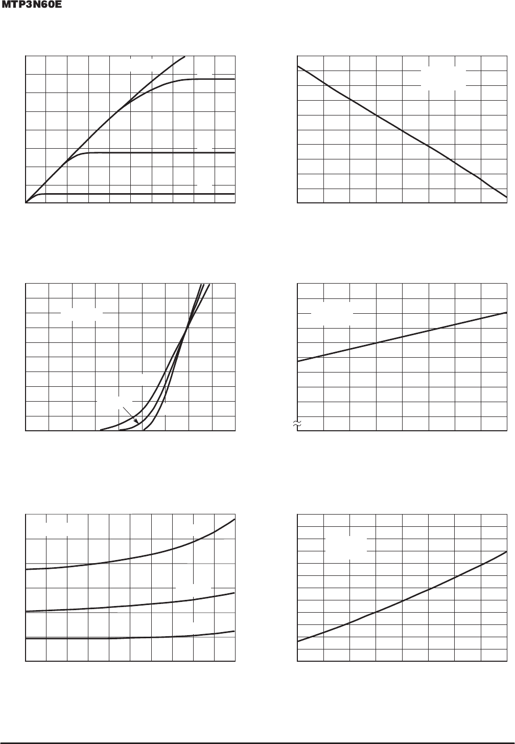
TYPICAL ELECTRICAL CHARACTERISTICS
V
DS
, DRAIN–TO–SOURCE VOLTAGE (VOLTS)
Figure 1. On–Region Characteristics
T
J
, JUNCTION TEMPERATURE (°C)
Figure 2. Gate–Threshold Voltage Variation
With Temperature
V
GS
, GATE–TO–SOURCE VOLTAGE (VOLTS)
Figure 3. Transfer Characteristics
T
J
, JUNCTION TEMPERATURE (°C)
Figure 4. Breakdown Voltage Variation
With Temperature
I
D
, DRAIN CURRENT (AMPS)
Figure 5. On–Resistance versus Drain Current
T
J
, JUNCTION TEMPERATURE (°C)
Figure 6. On–Resistance versus Temperature
R
DS(on)
, DRAIN–TO–SOURCE RESISTANCE (OHMS)
R
DS(on)
, DRAIN–TO–SOURCE RESISTANCE
(NORMALIZED)
I
D
, DRAIN CURRENT (AMPS)
V
GS(th)
, GATE THRESHOLD VOLTAGE (NORMALIZED)
V
BR(DSS)
, DRAIN–TO–SOURCE BREAKDOWN VOLTAGE
(NORMALIZED)
6
5
4
3
2
201612840
1.2
1.1
1
0.9
0.8
–50 –25 0 25 50 75 100 125 150
5
4
3
2
1
0
86420
1.2
1.1
1
0.9
0.8
–50 0 50 100 150
8
6
4
2
543210
2.5
2
1.5
1
0.5
T
J
= 25°C
7 V
6 V
5 V
V
DS
= V
GS
I
D
= 0.25 mA
T
J
= –55°C
25°C
100°C
V
GS
= 0
I
D
= 250 µA
T
J
= 100°C
25°C
–55°C
V
GS
= 10 V
V
GS
= 10 V
I
D
= 1.5 A
I
D
, DRAIN CURRENT (AMPS)
V
GS
= 10 V
4 V
V
DS
≥ 10 V
1
0
2 6 10 14 18
0
–50 –25 0 25 50 75 100 125 150
4–711
Motorola TMOS Power MOSFET Transistor Device Data
SAFE OPERATING AREA INFORMATION
I
D
, DRAIN CURRENT (AMPS)
I
D
, DRAIN CURRENT (AMPS)
V
DS
, DRAIN–TO–SOURCE VOLTAGE (VOLTS)
Figure 7. Maximum Rated Forward Biased
Safe Operating Area
V
DS
, DRAIN–TO–SOURCE VOLTAGE (VOLTS)
Figure 8. Maximum Rated Switching
Safe Operating Area
0 100 200 300 400
0
16
100
R
DS(on)
LIMIT
THERMAL LIMIT
PACKAGE LIMIT
10
V
GS
= 20 V
SINGLE PULSE
T
C
= 25°C
1
0.1
10
1 µs
1 ms
10 ms
12
4
600
8
1
0.01
100 µs
T
J
≤ 150°C
1000
10 µs
500
dc
FORWARD BIASED SAFE OPERATING AREA
The FBSOA curves define the maximum drain–to–source
voltage and drain current that a device can safely handle
when it is forward biased, or when it is on, or being turned on.
Because these curves include the limitations of simultaneous
high voltage and high current, up to the rating of the device,
they are especially useful to designers of linear systems. The
curves are based on a case temperature of 25°C and a maxi-
mum junction temperature of 150°C. Limitations for repetitive
pulses at various case temperatures can be determined by
using the thermal response curves. Motorola Application
Note, AN569, “Transient Thermal Resistance–General Data
and Its Use” provides detailed instructions.
SWITCHING SAFE OPERATING AREA
The switching safe operating area (SOA) of Figure 8 is the
boundary that the load line may traverse without incurring
damage to the MOSFET. The fundamental limits are the
peak current, I
DM
and the breakdown voltage, V
(BR)DSS
. The
switching SOA shown in Figure 8 is applicable for both turn–
on and turn–off of the devices for switching times less than
one microsecond.
Figure 9. Resistive Switching Time Variation
versus Gate Resistance
t,
TI
M
E
(
ns
)
R
G
, GATE RESISTANCE (OHMS)
V
DD
= 250 V
I
D
= 3 A
V
GS
= 10 V
T
J
= 25°C
t
f
t
r
t
d(off)
t
d(on)
10001
1
000
1
10
100
10 100
Figure 10. Thermal Response
r(t), EFFECTIVE TRANSIENT THERMAL
RESISTANCE (NORMALIZED)
R
θJC
(t) = r(t) R
θJC
R
θJC
= 2.5°C/W MAX
D CURVES APPLY FOR POWER
PULSE TRAIN SHOWN
READ TIME AT t
1
T
J(pk)
– T
C
= P
(pk)
R
θJC
(t)
P
(pk)
t
1
t
2
DUTY CYCLE, D = t
1
/t
2
t, TIME (ms)
1
0.01
0.2
D = 0.5
0.05
0.01
SINGLE PULSE
0.1
0.01
0.02
0.03
0.02
0.05
0.1
0.2
0.3
0.5
0.02 0.05 0.1 0.2 0.5 1 2 5 10 20 50 100 200 500 1000
0.7
0.07
0.03 0.3 3 30 300
I
D
, DRAIN CURRENT (AMPS)
Figure 12. Commutating Safe Operating Area (CSOA)
0 100 200 300 400
4
3
2
0
1
V
DS
, DRAIN-TO-SOURCE VOLTAGE (VOLTS)
+
+
–
Figure 13. Commutating Safe Operating Area
Test Circuit
V
R
V
GS
I
FM
20 V
R
GS
DUT
I
S
L
i
V
R
= 80% OF RATED V
DS
V
dsL
= V
f
+ L
i
⋅ dl
s
/dt
+
–
di/dt ≤ 50 A/µs
500
600
Figure 14. Unclamped Inductive Switching
Test Circuit
Figure 15. Unclamped Inductive Switching
Waveforms
t
L
V
DS
I
D
V
DD
t
P
V
(BR)DSS
V
DD
I
D(t)
C
4700 µF
250 V
R
GS
50 Ω
I
O
V
ds(t)
t, (TIME)
W
DSR
1
2
LI
O
2
V
(BR)DSS
V
(BR)DSS
–V
DD
V
DS
4–712
Motorola TMOS Power MOSFET Transistor Device Data
COMMUTATING SAFE OPERATING AREA (CSOA)
The Commutating Safe Operating Area (CSOA) of
Figure 12 defines the limits of safe operation for commutated
source-drain current versus re-applied drain voltage when
the source-drain diode has undergone forward bias. The
curve shows the limitations of I
FM
and peak V
R
for a given
commutation speed. It is applicable when waveforms similar
to those of Figure 11 are present. Full or half-bridge PWM DC
motor controllers are common applications requiring CSOA
data.
The time interval t
frr
is the speed of the commutation cycle.
Device stresses increase with commutation speed, so t
frr
is
specified with a minimum value. Faster commutation speeds
require an appropriate derating of I
FM
, peak V
R
or both. Ulti-
mately, t
frr
is limited primarily by device, package, and circuit
impedances. Maximum device stress occurs during t
rr
as the
diode goes from conduction to reverse blocking.
V
DS(pk)
is the peak drain–to–source voltage that the device
must sustain during commutation; I
FM
is the maximum for-
ward source-drain diode current just prior to the onset of
commutation.
V
R
is specified at 80% of V
(BR)DSS
to ensure that the
CSOA stress is maximized as I
S
decays from I
RM
to zero.
R
GS
should be minimized during commutation. T
J
has only
a second order effect on CSOA.
Stray inductances, L
i
in Motorola’s test circuit are assumed
to be practical minimums.
Figure 11. Commutating Waveforms
15
V
V
GS
0
90%
I
FM
dl
s
/dt
I
S
10%
t
rr
I
RM
t
on
V
DS
V
f
V
dsL
dV
DS
/dt
V
DS(pk)
MAX. CSOA
STRESS AREA
V
R
0.25 I
RM
4–713
Motorola TMOS Power MOSFET Transistor Device Data
GATE–TO–SOURCE OR DRAIN–TO–SOURCE VOLTAGE (VOLTS)
Figure 16. Capacitance Variation
C, CAPAC
IT
ANC
E
(p
F
)
V
GS
V
DS
0
C
iss
1
000
800
600
400
252010010
Figure 17. Gate Charge versus
Gate–To–Source Voltage
Q
G
, TOTAL GATE CHARGE (nC)
16
0
05
12
8
4
10 15 20 25
200
Figure 18. Gate Charge Test Circuit
V
in
15 V
100 k
47 k
2N3904
2N3904
1 mA
+18 V V
DD
10 V
100 k
0.1 µF
100
FERRITE
BEAD
DUT
SAME
DEVICE TYPE
AS DUT
V
in
= 15 V
pk
; PULSE WIDTH ≤ 100 µs, DUTY CYCLE ≤ 10%
T
J
= 25°C
V
GS
= 0
47 k
V
DS
= 100 V
V
GS
, GATE–TO–SOURCE VOLTAGE (VOLTS)
250 V
5515
V
DS
= 0
T
J
= 25°C
I
D
= 3 A
400 V
C
oss
C
rss
4–714
Motorola TMOS Power MOSFET Transistor Device Data
N–Channel Enhancement–Mode Silicon Gate
This advanced high voltage TMOS E–FET is designed to
withstand high energy in the avalanche mode and switch efficiently.
This new high energy device also offers a drain–to–source diode
with fast recovery time. Designed for high voltage, high speed
switching applications such as power supplies, PWM motor
controls and other inductive loads, the avalanche energy capability
is specified to eliminate the guesswork in designs where inductive
loads are switched and offer additional safety margin against
unexpected voltage transients.
• Avalanche Energy Capability Specified at Elevated
Temperature
• Low Stored Gate Charge for Efficient Switching
• Internal Source–to–Drain Diode Designed to Replace External
Zener Transient Suppressor — Absorbs High Energy in the
Avalanche Mode
• Source–to–Drain Diode Recovery Time Comparable to Discrete
Fast Recovery Diode
MAXIMUM RATINGS
(T
C
= 25°C unless otherwise noted)
Rating Symbol Value Unit
Drain–Source Voltage V
DSS
600 Vdc
Drain–Gate Voltage (R
GS
= 1.0 MΩ) V
DGR
600 Vdc
Gate–Source Voltage — Continuous
Gate–Source Voltage — Non–repetitive
V
GS
V
GSM
±20
±40
Vdc
Vpk
Drain Current — Continuous
Drain Current — Pulsed
I
D
I
DM
3.0
14
Adc
Total Power Dissipation @ T
C
= 25°C
Derate above 25°C
P
D
75
0.6
Watts
W/°C
Operating and Storage Temperature Range T
J
, T
stg
–55 to 150 °C
UNCLAMPED DRAIN–TO–SOURCE AVALANCHE CHARACTERISTICS (T
J
< 150°C)
Single Pulse Drain–to–Source Avalanche Energy — T
J
= 25°C
Single Pulse Drain–to–Source Avalanche Energy — T
J
= 100°C
Repetitive Pulse Drain–to–Source Avalanche Energy
W
DSR(1)
W
DSR(2)
290
46
7.5
mJ
THERMAL CHARACTERISTICS
Thermal Resistance — Junction to Case°
Thermal Resistance — Junction to Ambient°
R
θJC
R
θJA
1.67
62.5
°C/W
Maximum Lead Temperature for Soldering Purposes, 1/8″ from case for 10 seconds T
L
260 °C
(1) V
DD
= 50 V, I
D
= 3.0 A
(2) Pulse Width and frequency is limited by T
J
(max) and thermal response
Designer’s Data for “Worst Case” Conditions — The Designer’s Data Sheet permits the design of most circuits entirely from the information presented. SOA Limit
curves — representing boundaries on device characteristics — are given to facilitate “worst case” design.
Preferred devices are Motorola recommended choices for future use and best overall value.
REV 1
SEMICONDUCTOR TECHNICAL DATA
TMOS POWER FET
3.0 AMPERES
600 VOLTS
R
DS(on)
= 2.2 OHMS
D
S
G
CASE 221A–06, Style 5
TO-220AB
Motorola Preferred Device
4–715
Motorola TMOS Power MOSFET Transistor Device Data
ELECTRICAL CHARACTERISTICS (T
J
= 25°C unless otherwise noted)
Characteristic
Symbol Min Typ Max Unit
OFF CHARACTERISTICS
Drain–to–Source Breakdown Voltage
(V
GS
= 0, I
D
= 250 µAdc)
V
(BR)DSS
600 — — Vdc
Zero Gate Voltage Drain Current
(V
DS
= 600 V, V
GS
= 0)
(V
DS
= 480 V, V
GS
= 0, T
J
= 125°C)
I
DSS
—
—
—
—
0.25
1.0
mAdc
Gate–Body Leakage Current — Forward (V
GSF
= 20 Vdc, V
DS
= 0) I
GSSF
— — 100 nAdc
Gate–Body Leakage Current — Reverse (V
GSR
= 20 Vdc, V
DS
= 0) I
GSSR
— — 100 nAdc
ON CHARACTERISTICS*
Gate Threshold Voltage
(V
DS
= V
GS
, I
D
= 250 µAdc)
(T
J
= 125°C)
V
GS(th)
2.0
1.5
—
—
4.0
3.5
Vdc
Static Drain–to–Source On–Resistance (V
GS
= 10 Vdc, I
D
= 1.5 A) R
DS(on)
— 2.1 2.2 Ohms
Drain–to–Source On–Voltage (V
GS
= 10 Vdc)
(I
D
= 3.0 A)
(I
D
= 1.5 A, T
J
= 100°C)
V
DS(on)
—
—
—
—
9.0
7.5
Vdc
Forward Transconductance (V
DS
= 15 Vdc, I
D
= 1.5 A) g
FS
1.5 — — mhos
DYNAMIC CHARACTERISTICS
Input Capacitance
(V 25 V V 0
C
iss
— 770 — pF
Output Capacitance
(V
DS
= 25 V, V
GS
= 0,
f = 1.0 MHz
)
C
oss
— 105 —
Transfer Capacitance
f
1.0
MHz)
C
rss
— 19 —
SWITCHING CHARACTERISTICS*
Turn–On Delay Time t
d(on)
— 23 — ns
Rise Time
(V
DD
= 300 V, I
D
≈ 3.0 A,
R
L
= 100 Ω R
G
=12Ω
t
r
— 34 —
Turn–Off Delay Time
R
L
=
100
Ω
,
R
G
=
12
Ω
,
V
GS
(
on
)
= 10 V)
t
d(off)
— 58 —
Fall Time
GS(on)
t
f
— 35 —
Total Gate Charge
(V 420 V I 3 0 A
Q
g
— 28 31 nC
Gate–Source Charge
(V
DS
= 420 V, I
D
= 3.0 A,
V
GS
= 10 V
)
Q
gs
— 5.0 —
Gate–Drain Charge
V
GS
10
V)
Q
gd
— 17 —
SOURCE–DRAIN DIODE CHARACTERISTICS
Forward On–Voltage V
SD
— — 1.4 Vdc
Forward Turn–On Time
(I
S
= 3.0 A, di/dt = 100 A/µs)
t
on
— ** —
ns
Reverse Recovery Time t
rr
— 400 —
INTERNAL PACKAGE INDUCTANCE
Internal Drain Inductance
(Measured from the contact screw on tab to center of die)
(Measured from the drain lead 0.25″ from package to center of die)
L
d
—
—
3.5
4.5
—
—
nH
Internal Source Inductance
(Measured from the source lead 0.25″ from package to source bond pad)
L
s
— 7.5 —
*Pulse Test: Pulse Width = 300 µs, Duty Cycle ≤ 2.0%.
**Limited by circuit inductance.
4–716
Motorola TMOS Power MOSFET Transistor Device Data
TYPICAL ELECTRICAL CHARACTERISTICS
V
DS
, DRAIN–TO–SOURCE VOLTAGE (VOLTS)
Figure 1. On–Region Characteristics
T
J
, JUNCTION TEMPERATURE (°C)
Figure 2. Gate–Threshold Voltage Variation
With Temperature
V
GS
, GATE–TO–SOURCE VOLTAGE (VOLTS)
Figure 3. Transfer Characteristics
T
J
, JUNCTION TEMPERATURE (°C)
Figure 4. Breakdown Voltage Variation
With Temperature
I
D
, DRAIN CURRENT (AMPS)
Figure 5. On–Resistance versus Drain Current
T
J
, JUNCTION TEMPERATURE (°C)
Figure 6. On–Resistance Variation
With Temperature
R
DS(on)
, D
R
A
I
N
–T
O
–
SO
UR
C
E
RE
S
I
S
T
ANC
E
(
O
H
MS
)
R
DS(on)
, DRAIN–TO–SOURCE ON–RESISTANCE
(NORMALIZED)
I
D
, D
R
A
I
N C
URRE
N
T
(
AMPS
)
V
GS(th)
, GATE THRESHOLD VOLTAGE (NORMALIZED)
V
BR(DSS)
, DRAIN–TO–SOURCE BREAKDOWN VOLTAGE
(NORMALIZED)
8
6
4
2
201612840
1.2
1.1
1
0.9
0.8
–50 –25 0 25 50 75 100 125 150
10
8
6
4
0
86420
1.2
1.1
1
0.9
0.8
–50 0 50 100 150
6
2
0
106420
7 V
6 V
5 V
V
DS
= V
GS
I
D
= 0.25 mA
T
J
= 25°C
–55°C
100°C
V
GS
= 0
I
D
= 250 µA
V
GS
= 10 V
V
GS
= 10 V
I
D
= 2 A
I
D
, D
R
A
I
N C
URRE
N
T
(
AMPS
)
V
GS
= 10 V
0.7
V
DS
≥ 10 V
1 3 5 7 9 –25 25 75 125
–50 0 50 100 150–25 25 75 125
0
4
T
J
= 25°C
–55°C
100°C
3
0
2
1
2 6 10 14 18
2
8
4–717
Motorola TMOS Power MOSFET Transistor Device Data
SAFE OPERATING AREA INFORMATION
I
D
, DRAIN CURRENT (AMPS)
I
D
, DRAIN CURRENT (AMPS)
V
DS
, DRAIN–TO–SOURCE VOLTAGE (VOLTS)
Figure 7. Maximum Rated Forward Biased
Safe Operating Area
V
DS
, DRAIN–TO–SOURCE VOLTAGE (VOLTS)
Figure 8. Maximum Rated Switching
Safe Operating Area
0 200 400
0
16
100
R
DS(on)
LIMIT
THERMAL LIMIT
PACKAGE LIMIT
10
V
GS
= 20 V
SINGLE PULSE
T
C
= 25°C
1
100
10 µs
1 ms
10 ms
800
10
1
0.1
100 µs
T
J
≤ 150°C
1000
12
8
4
600
dc
FORWARD BIASED SAFE OPERATING AREA
The FBSOA curves define the maximum drain–to–source
voltage and drain current that a device can safely handle
when it is forward biased, or when it is on, or being turned on.
Because these curves include the limitations of simultaneous
high voltage and high current, up to the rating of the device,
they are especially useful to designers of linear systems. The
curves are based on a case temperature of 25°C and a maxi-
mum junction temperature of 150°C. Limitations for repetitive
pulses at various case temperatures can be determined by
using the thermal response curves. Motorola Application
Note, AN569, “Transient Thermal Resistance–General Data
and Its Use” provides detailed instructions.
SWITCHING SAFE OPERATING AREA
The switching safe operating area (SOA) of Figure 8 is the
boundary that the load line may traverse without incurring
damage to the MOSFET. The fundamental limits are the
peak current, I
DM
and the breakdown voltage, V
(BR)DSS
. The
switching SOA shown in Figure 8 is applicable for both turn–
on and turn–off of the devices for switching times less than
one microsecond.
The power averaged over a complete switching cycle must
be less than:
T
J(max)
– T
C
R
θJC
Figure 9. Resistive Switching Time
Variation versus Gate Resistance
t,
TI
M
E
(
ns
)
R
G
, GATE RESISTANCE (OHMS)
V
DD
= 300 V
I
D
= 3 A
V
GS(on)
= 10 V
T
J
= 25°C
t
f
t
r
t
d(off)
t
d(on)
10001
1
0000
10
100
1000
10 100
Figure 10. Thermal Response
r(t), NORMALIZED EFFECTIVE
TRANSIENT THERMAL RESISTANCE
R
θJC
(t) = r(t) R
θJC
R
θJC
= 1.67°C/W MAX
D CURVES APPLY FOR POWER
PULSE TRAIN SHOWN
READ TIME AT t
1
T
J(pk)
– T
C
= P
(pk)
R
θJC
(t)
P
(pk)
t
1
t
2
DUTY CYCLE, D = t
1
/t
2
t, TIME (ms)
1
0.01
D = 0.5
0.05
0.01
SINGLE PULSE
0.01
0.02
0.03
0.02
0.05
0.1
0.2
0.3
0.5
0.02 0.05 0.1 0.2 0.5 1 2 5 10 20 50 100 200 500 1 k
0.2
0.1