Vij D.R. Handbook of Applied Solid State Spectroscopy
Подождите немного. Документ загружается.

and resulted in their receiving the Nobel Prize in 1986 [23].
From the STM has evolved an entire menagerie of scanning probe
microscopy (SPM) techniques. While this chapter is solely concerned with
STM, it is useful to introduce it by way of the more general SPM approach. A
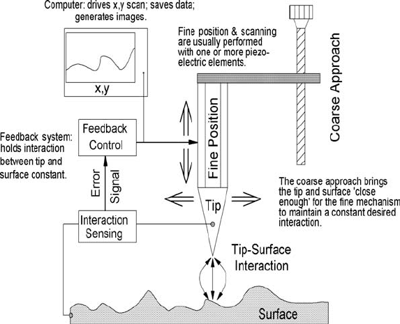
schematic representation of the essential elements for any scanning probe
microscope is presented in Figure 7.2. The tip-sample interaction defines the
type of SPM and controls the spatial resolution possible with the particular
technique. For example, if mechanical forces are measured by physical
contact between tip and sample, then the radius of curvature of the tip and the
elastic compliance of the substrate limit the possible spatial resolution in the
Figure 7.2 Schematic representation of a scanning probe microscope. The critical element in
differentiating the different probe techniques and their relative resolutions is the tip-surface
interaction and the method of sensing that interaction. In STM it is the tunneling current that is
sensed.
In STM it is the tunneling current that is probed. The exponential
dependence of the current on tip-sample separation results in the possibility of
single atom resolution. This is generally explained by considering a tip
formed from a single atom sitting in a three-fold hollow site. For conditions
about 90% of the current is carried by the apical atom because of the
difference in distance between it and the atoms at its base. For the general
7. Scanning Tunneling Spectroscopy (STS)
resolution image of two unit cells of the 7 × 7 reconstruction surface of
silicon
(x, y)-plane.
normally used in high resolution STM (1 nA set point and 300 mV bias),
308
(111). It was this image that captured the attention of the surface science
world
7.2 The Scanning Tunneling Microscope (STM)
resolution. Good STM tips are generally atomically sharp and methods for
fabricating them will be discussed later. On the other hand, the z (or normal
direction) resolution depends solely upon the z dependence of the interaction
between tip and sample. Because of its exponential form, STM is the most
sensitive SPM technique, easily achieving 0.005-nm sensitivity.
Another essential feature of all SPMs is the feedback control loop. This
electronic system maintains the tip-sample interaction at a preset value by
controlling the z position (or deflection) of the tip relative to the surface (or to
an undeflected position). In the case of the STM, the absolute distance of the
tip from the surface is difficult to impossible to determine, and the relative
height is controlled through setting fixed values of current and voltage (I ~ cV
exp(–d )
1/2
)). Typical current values range from picoamps to nanoamps,
while the bias voltage can vary from millivolts to volts. Commercial feedback
loops generally incorporate both integral and proportional gain stages. As in
all feedback loop applications, it is desirable to set the gain as high as possible
but not so high as to drive the system into oscillation. Oscillation of the
feedback loop is especially bad in STM where repeated contacts between tip
and surface (called “crashes”) can destroy the usefulness of the tip.
The SPM image is generated by performing a raster scan of the tip over the
surface while recording the z deflection required to maintain the set-point.
Almost all commercial instruments use one or more piezoelectric elements to
perform the fine motion required to generate images with sub Angstrom data
intervals. Instruments designed for high resolution are usually limited to
piezoelectric elements having 1 to 10 micron maximum scan widths, while
100 micron scan widths are available for lower resolution SPM studies. It is
important to note that in the feedback controlled scan regime, one is almost
never measuring a true height. In STM, for example, the changes in tip height
with position under feedback control reflect both the tip-sample separation
and the spatial variation of the local density of surface states (LDOS) of the
reflects true height changes if the LDOS of the surface (the local work
function) is constant across the surface. This would be the case for atomic
steps on clean metal surfaces, but would NOT be the case for adsorbates on
surfaces.
The range of z motion possible for the fine position control is generally
only a few microns. Thus, some method of bringing the tip within a few
microns of the surface without crashing it is required. This is identified as the
accomplished by a fine pitch screw (as in the Veeco electrochemical STM
[24]), or a piezoelectric driven slip-stick (inertial approach) mechanism (as in
coarse approach mechanism, as does the RHK design [26].
The computer control system does more than integrate the feedback loop
with the scanning mechanism while saving piezoelectric position coordinates.
SPM technique, the finer one can make the tip, the higher the x, y spatial
sample ()(x, y) in the simple model). Thus, the constant current image only
coarse approach mechanism in Figure 7.2. Often, this course approach is
the McAllister [25]). Some designs incorporate x, y coarse motion into their
309
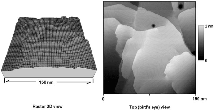
Another essential feature is in displaying the data in a manner easily
interpreted by the human eye. The left hand image of Figure 7.3 shows the
STM constant current height versus position of a large area of a Au-111
surface. While the data were actually acquired with a 512 × 512 grid, only a
small sampling of the grid is shown for clarity. The change in tip height
relative to the initial set-point at each grid crossing is mapped both as a 3D
projection and by brightness. The lighter the area, the higher the feature.
Figure 7.3 Comparison of different display methods for the same data set of constant current
height versus position for the same large area of a Au-111 surface. The left hand image shows a
portion of the 512 x 512 grid used for data collection with the heights mapped both as a 3D
projection and by brightness. The right hand image is a standard top view where all the height
information is contained in the gray scale shown to the far right.
While these 3D projection images are lovely, a real appreciation of the
data requires the ability to rotate and tilt the image interactively relative to the
observer. Almost all modern SPM software is capable of doing this real time,
but this interactive image is not something that can be placed in a publication.
Instead, a top view, sometimes called a “bird's eye view,” is most frequently
published. The right hand image is a standard top view of the same area as
shown in the left image. Here, all the height information is contained in the
While virtually any commercial STM will do a good job of taking pictures
of surfaces, spectroscopic applications place extra requirements on the
instrumentation that must be met if even low quality data are desired.
1) The control and data acquisition system must be able to ramp the bias
voltage or the tip sample separation while acquiring the tunneling current or
some other voltage signal supplied by an external device. The rate at which
data are acquired must be variable over a wide range in time (from about 5
microseconds to about 10 milliseconds per data point), in voltage (from about
7. Scanning Tunneling Spectroscopy (STS) 310
color scale, which is displayed to the far right.
7.2 The Scanning Tunneling Microscope (STM)
r0.5 volt to r10.0 volts, with the ability to set asymmetrical limits being
highly desirable), or in z span (from about –2 nm to +5 nm, where negative
distance moves the tip closer to the substrate than at the set-point. The most
commonly used auxiliary input is the output of a lock-in amplifier that detects
a modulated signal in the tip current.
2) It must be possible to add modulation (typically sine or square wave) to
the bias or tip position voltage. An old version of the Digital Instruments
(now Veeco) software, version 3.2x, had built in square wave modulation and
the software could display directly dI/dV, determined from the resulting
modulation in the current. This system worked very well, but was dropped
from, or incorrectly implemented in, later versions of the software. To our
knowledge, none of today’s manufacturers offer such complete “built-in”
spectroscopic capability.
3) The control system must be able to shut off the feedback loop during
data acquisition, when desired.
4) The drift (both x, y and z) must be low. The extent of acceptable x, y
drift is determined by the amount of spatial resolution desired for the
spectroscopic data. If one is acquiring spatially averaged molecular spectra
from a dense monolayer with a large curvature tip, drifts of the order of
atoms through their vibrational signature in STM-based IETS, drifts of less
than 0.05 nm/min are required. The amount of acceptable drift in the z
direction is determined by the intensity of the spectral feature to be studied
relative to the background tunneling current in the absence of that feature.
Since this background increases (approximately) as I and I = CV exp(–
Az)), a small change in z, dz, results in an increase in relative current (dI/I)
of –A)dz. Or, using z in nm and ) in volts, the background change in
relative current with a small z drift of dz is given by dI/I ~ –0.1 dz. For true
vibrational IETS (with no resonance enhancements), dI/I for the spectral
transition, dI/I ~ 0.002. Thus, less than 1 × 10
–2
nm of z drift is allowed during
the time required to scan a particular spectral band. For STM-OMTS, on the
other hand, dI/I ~ 0.1, and 100 times as much z drift is allowed. Moreover,
because the OMTS signal is so much stronger than that of IETS, equal signal-
to-noise can be obtained about (0.1/0.002)
1/2
~ 7 times faster. Overall, STM-
OMTS is expected to be about 1000 times less z drift-sensitive than STM-
IETS of non-resonance enhanced transitions.
5) Sample and tip geometry and shielding: Because of the drift constraints
discussed above, one needs to take spectra as fast as the electronic bandwidth
allows. With the feedback loop turned off, the limiting term is the capacitance
in the tip-sample assembly and the wires leading to the preamplifier circuit.
Thus, the preamplifier needs to be close to the tip, and the tip and sample need
to be electrically isolated and as small as possible.
6) An essential requirement for STM-IETS is that the working parts of the
STM be at or below 10 K. Otherwise, the thermal line-width destroys the
information inherent in identifying vibrational peak positions. It is not enough
1 nm/s can be tolerated. On the other hand, if one is trying to locate particular
311
to cool the sample; the sample, tip, and all parts physically close must be
cooled to this temperature. In the case of STM-based OMTS or spectroscopic
studies of density of states in metals or semiconductors, room temperature
measurements are usually satisfactory, and many measurements can be made
at significantly elevated temperatures.
7.2.1 Commercial Instruments
There are currently available a wide range of SPM instruments that
incorporate all of the features discussed above (except for tips, which we will
discuss later). A number of commercial suppliers, many of whom currently
only provide atomic force microscopy (AFM) instruments and not STM, are
listed below. It may be noted, however, that this is a rapidly evolving business
and companies may broaden or narrow their offerings on short notice. This
list is not exhaustive and the absence of a manufacturer from the list does not
indicate any preference. In the United States, Veeco Metrology [24] is the
major supplier of ambient and solution phase SPMs, followed by Molecular
Imaging Corporation [27]. Asylum Research is an offshoot the original
Digital Instruments (now owned by Veeco) and specializes AFM and pico-
force measurements [28]. Novascan provides ambient scanning force
microscopes, AFM tips, and chemically modified tips and samples [29].
Quesant, in partnership with Novascan, provides a full range of ambient and
liquid scanning probe microscopes [30]. For UHV systems made in the
United States, one must turn either to McAllister Technical [25] or RHK
Technology [26]. The McAllister system is very inexpensive and has provided
very high resolution images in the hands of a number of research groups, but
it is a room temperature-only STM. RHK now offers both STM and AFM in
UHV with variable temperature achieved by cooling the sample (only). Note,
as indicated in a previous section, that for the purposes of measuring
vibrational inelastic spectroscopy the entire microscope (sample and tip) must
be cooled. To our knowledge there are currently no U.S. suppliers of such
microscopes. While commenting on spectroscopy, it is useful to note that
STM heads where the sample and tip are electrically isolated from the rest of
the microscope (including the sample holder) are especially desirable for
spectroscopic purposes. These designs (like that of the RHK) minimize the
capacitive coupling that can limit the sampling speed.
The best-known UHV STM and AFM system provider is the German
company, Omicron [31]. Omicron offers a range of UHV systems with cooled
sample STM and AFM capability, and the multiprobe LT which is a dedicated
low temperature STM wherein both the tip and sample are cooled. Witech
is another German company that makes commercial AFM and SNOM
equipment, but appears to have dropped their STM line [32]. Nanosurf is a
Swiss company that manufactures extremely compact and inexpensive STM
and AFM systems suitable for use in undergraduate laboratories [33]. Both
7. Scanning Tunneling Spectroscopy (STS) 312
7.2 The Scanning Tunneling Microscope (STM)
Witech and Nanosurf are respresented in the United States by Nanoscience
Instruments [34]. Nanotech Electronica is a Spanish company specializing in
scanning force microscopy and distributing a free SPM (including STM) data
analysis program WSxM [35]. In Russia, NT-MDT is a comprehensive
supplier of STM and AFM instruments and supplies, and it also offers a small
education-oriented multipurpose scanning probe microscope [36] Other SPM
manufacturers include Danish Micro Engineering [37], JPK [38] and
Attocube [39] instruments specializing in AFM and SNOM, PSIA in Korea
specializing in AFM [40], and in Germany, SIS offering ambient AFM
systems [41] and Triple-O offering AFM and SNOM systems [42].
7.2.3 Tips
Once an appropriate SPM has been purchased or built from scratch, one must
obtain appropriate tips and samples. Since the emphasis here is on STM,
suffice it to say that there are a number of commercial sources for silicon,
silicon nitride, and variously coated tips appropriate for scanning force
microscopy [24, 29, 34, 36, 43]. While research grade AFM tips are
commercially available at reasonable prices, this is not the situation for
STM.While a few companies offer etched STM tips, they are expensive and
generally unsuitable for spectroscopic applications because of their long
exposure to various ambient environments. Thus, the STM practitioner makes
his own tips. These fall generally into two classes, mechanically formed and
etched tips.
The first STM tips were mechanically formed by Binnig et al. [44, 45].
These were formed by mechanical grinding (at 90q!) 1-mm diameter tungsten
wire. Today, by far the most common mechanically formed tips are cut wire
tips. While Au, Pt
0.9
Ir
0.1
, Pt
1–x
Rh
x
, and similar metal wires have been used, the
most popular cut tip is made from 0.25-mm diameter Pt
0.8
Ir
0.2
wire. Almost
every laboratory has its own preferred cutting method. Some anneal the wire
before cutting with dull scissors using a pulling motion. Others prefer to use
very sharp dykes. Some suggest that a 60q angle cut is best, while others
prefer larger or smaller angles. Since the “tip” is really an atomic asperity at
the end of a rather rough mass of metal, it is not too surprising that the
macroscopic and microscopic (as in microns) morphology have little
relevance to the quality of the tip. In fact, the tips that give the best images do
not always appear sharp under an optical microscope (200 to 400 power).
There are almost always a number of tips like fingers of a hand extending
towards the surface. See, for example, Figure 6.4a in reference [46]. Because
of the strong exponential dependence of the tunneling current, only the
longest “finger” is important when measuring flat surfaces. When imaging
rough surfaces, or intermediate to large features (a nm or more tall) on a flat
surface, one may see “ghost images” resulting from tunneling through
313
secondary tips of nearly the same length as the longest. The offset between
the ghost and the primary image is related to the offset between the longest
and second longest asperity. The cure for ghost images is to re-cut the tip until
the ghosts disappear. Cut Pt
0.8
Ir
0.2
tips are inexpensive, quickly made, and
have a fairly good yield (usually 1 in 2 will show atomic reconstruction lines
on Au).
Electrochemically etched tips offer a well-defined geometry near the
atomic asperity that functions as the tip. Methods for preparing atomically
sharp tips from a number of different metals were first developed primarily
for field ion microscopy [47, 48]. Etched tips are commonly made from Pt, Ir,
Au, W, Pd, Ni, and Ag. Prescriptions for a number of these metals were given
etched Pt
0.8
Ir
0.2
tips are preferred. Various methods for making these are
described in the literature [49–52], including descriptions of how to limit
Faradaic currents through tip coating [53, 54]. Au tips, both etched [55, 56]
and coated [57] have been reported in the literature, as have etched silver tips
[58]. For spin-polarized tunneling studies, Cavallini reports that etched nickel
tips work well and have better oxidation resistance than tungsten tips [59]. By
far the most commonly used tip material for UHV studies is tungsten, and
these tips are almost always etched tips.
One has a great variety of methods to choose from when etching W tips
[49, 60–62]. One may either follow the prescriptions and designs in the
literature, or purchase commercial tip etching stands such as those offered by
W-tech (through Omicron) or Shrodinger's Sharpener from Obbligato
Objectives [63]. Electrochemically etched W tips have an oxide layer on the
surface. This oxide layer can be up to 20 nm thick [64]. Dipping the W tips in
47% HF prior to loading in the UHV chamber has been reported to improve
tips [65–67], but an insulating layer is still apparently left on the tip surface
[65, 67]. For simple imaging, the oxide layer on freshly prepared tips is
usually not a problem. For spectroscopic studies, however, it is a major
impediment since the spectrum can be dominated by the density of states of
the oxide layer. The stable form of the oxide is WO
3
, and can be removed by
heating above 800 C [68]. At this temperature WO
3
reacts with W to form
WO
2
, which then sublimes. W melts at 3410 C, so a wide window exists to
remove the oxide without deforming the tip. A convenient method of heating
the tip to remove contaminants is to use electron bombardment. However care
still needs to be taken since the local temperature at the tip can easily reach
the melting point – even to the extent of forming an obvious round ball at the
end of the tip wire.
Some crude in situ methods for tip cleaning have also been successful. In
the earliest days of STM, it was found that applying a 10 kHz 2 nm peak to
peak (vertical) oscillation to a tip initially in contact with a platinum plate
could produce clean sharp tips [44]. Binnig thought that this procedure might
clean the tip through some type of ultrasonic interaction. The application of a
large voltage pulse (from 3 volts to hundreds of volts) has also been used for
7. Scanning Tunneling Spectroscopy (STS) 314
by Nam et al. [49]. For solution, and especially electrochemical applications,
7.3 STS of Semiconductors & Metals
tip cleaning. Field emission cleaning is proposed to account for why
application of about 100 V between tip and sample at a distance suitable to
produce nA to mA currents can result in clean tips. In the above two cases,
one had best use either a clean portion of the sample (that is sacrificed), or
another clean metal sample. Another common method for eliminating the
oxide involves 'controlled' crashing of the tip on a clean gold surface. This
method does work on occasion, but it can also lead to dull (poor resolution) or
even bent (unrealistic surface images) tips. An extreme example of this is to
simply let the tip scan over a large area of the surface for an extended time.
For all the methods of this paragraph, it is not clear whether one cleans the W,
or coats the tip with the metal counter surface.
7.3 STS OF SEMICONDUCTORS & METALS
The scanning tunneling spectroscopy of metals and semiconductors primarily
focuses on elastic tunneling current changes associated with the local density
of states (LDOS), U
s
(r, E), which appears in equation (7.2). To a good
approximation, U
s
(r, E) is proportional to dI/dV when the tip is far from the
substrate and the density of states of the tip is reasonably smooth. These are
elastic tunneling spectra, as will be described in a later section.
Jacklevic and coworkers first demonstrated imaging of metal surface states
They found that the surface state peak was centered just above –500 mV
sample bias with a full width at half height of about 300 mV. They observed
changes in the peak intensity and position that correlated with surface
features. The surface state intensity was found to be substantially reduced at
step edges as compared to values observed for large terraces. A change in the
intensity by a factor of 2 over the 23 ×
3 reconstruction unit cell was also
observed. These effects were attributed to a spatial variation of the surface
state intensity with the local potential. Upward shifts of the surface state
energy were also observed on narrow terraces. Kuk and Silverman performed
tunneling spectroscopy of Au(100)-(5 × 20) and Fe on Au(100) surfaces [71].
were obtained (d is the tip – Au separation). The results confirmed that the
characteristics of the spectra resemble those of previously reported
semiconductors. From I – d relations, they found that the tunneling barrier
decreased abruptly when the tunneling gap was < 0.6 nm. Later, Kuk
reviewed the elastic scanning tunneling spectroscopy of a number of clean
metal surfaces [72]. He presented the operating principles of the scanning
tunneling microscope as applicable to the problem of the small corrugations
seen on metallic samples. Various spectroscopies were described and
compared with theory. Some examples of past accomplishments on metal
surfaces were given.
Using a well-defined tunneling tip, I – d, I – V, and dlnI/dlnV – V spectra
315
when they identified the Au(111) surface state in its dI/dV spectrum [69, 70].
Fonden and coworkers investigated unoccupied surface resonances seen in
a plot of dI/dV versus V [73]. The authors extend and detail a previously
developed model for formation of electronic resonances at free electron-like
metal surfaces to calculate scanning tunneling spectra. The effect of the tip is
mimicked by inclusion of an external field, self-consistently, in a jellium
description of the surface potential. The lattice-induced corrugation of the
potential is included perturbatively via a pseudopotential. The authors
compare the calculated spectra for Al(111) with experimental results and
conclude that a peak occurring below the metal vacuum level is a “crystal-
derived” resonance, in the sense that lattice effects are crucial for its
manifestation. Hoermandinger [74] and Doyen and Drakova [75] also
investigated the theoretical underpinnings for the observation of metallic
surface states by dI/dV spectroscopy.
Bischoff and coworkers examined the role of impurities on the surface
state of V(001) [76]. They reported the first scanning tunneling spectroscopy
measurements on V(001). A strong surface state was detected that was very
sensitive to the presence of segregated carbon impurities. This surface state
energy shifted from 0.03 eV below the Fermi level in clean regions, up to as
much as +0.2 eV above the Fermi level in contaminated areas. Because of the
negative dispersion of this state, the upward shift could not be described in a
simple confinement picture. Rather, Bischoff concluded that the surface state
energy was governed by vanadium surface s-d interactions, which are altered
by carbon coverage. Differences in the tunneling spectra of metals have been
used to provide chemical selectivity for one metal on another [77, 78].
Himpsel and coworkers studied the growth of copper stripes on stepped
W(110) and Mo(110) surfaces. Contrast between copper and the substrate
metal was achieved by resonant tunneling via surface states and image
states.These states are characterized independently by inverse photoemission.
Image states provide elemental identification via the work function, since
their energy is correlated with the local work function. Element-specific
surface states produce contrast at higher spatial resolution, but the contrast is
smaller than that for image states [77]. Weisendanger and coworkers studied
the topography and chemical surface structure of a submonolayer Fe film on a
W(110) substrate by combined STM and spectroscopy [78]. Local tunneling
spectra revealed a pronounced difference in the electronic structure between
nanometer-scale Fe islands of monolayer height and the bare W(110)
substrate. In particular, a pronounced empty-state peak at 0.2 eV above the
Fermi level was identified for the Fe islands. Based on the pronounced
difference in the local tunneling spectra measured above the Fe islands and
the W substrate, element-specific imaging was achieved. Scanning tunneling
spectroscopy has also permitted real-space observation of one-dimensional
electronic states on an Fe(100) surface alloyed with Si [79]. These states are
localized along chains of Fe atoms in domain boundaries of the Fe(100)
7. Scanning Tunneling Spectroscopy (STS)
c(2 × 2)Si surface alloy. The calculated spin charge densities illustrate the
316
7.3 STS of Semiconductors & Metals
a two-dimensional state existing on the pure Fe(100) surface.
Scanning tunneling spectroscopy can also be used to study small metallic
structures on surfaces. Scanning tunneling spectroscopy and microscopy show
that the empty states of linear Au clusters supported on a metal surface behave
as if they are the states of an electron in an empty one-dimensional box [80].
It was suggested that certain difficulties of this description are removed by a
particle-in-a-cylinder model. Their interpretation was supported by density
functional calculations. Crommie et al. [81] studied the local properties of
low-dimensional electrons (properties such as standing wave patterns in the
surface local density of states, which is due to the quantum mechanical
interference of surface state electrons scattering off of step edges and
adsorbates). The authors found that Fe adatoms strongly scatter the surface
state and, as a result, are good building blocks for constructing atomic-scale
barriers (“quantum corrals”) to confine the surface state electrons. Tunneling
spectroscopy performed inside of the corrals reveals discrete resonances,
consistent with size quantization [81].
The potential of spin-polarized scanning tunneling microscopy and
spectroscopy (SP-STM/S) was by demonstrated Wiesendanger and coworkers
[82, 83] on antiferromagnetic and ferromagnetic transition metals and on rare
earth metals. Data measured on the antiferromagnetic Cr(001) surface
revealed that screw dislocations cause topology-induced spin frustrations
leading to the formation of domain walls with a width of about 120 nm [82].
On another antiferromagnetic surface a pseudomorphic monolayer film of
chemically identical manganese atoms on W(110), they showed that SP-STM
provides the surface magnetic structure with atomic resolution. SP-STS also
allows the imaging of the domain structure of self-organized Fe
nanostructures, which are antiferromagnetically coupled due to dipolar
interaction. Using spin-polarized scanning tunneling microscopy in an
external magnetic field, the Wiesendanger’s group observed magnetic
hysteresis on a nm scale in an ultrathin ferromagnetic film [83]. The film was
an array of Fe nanowires two atomic layers thick grown on a stepped W(110)
substrate. The microscopic sources of hysteresis in this system (domain wall
motion, domain creation, and domain annihilation) were observed with nm
spatial resolution [83]. A saturation field stable residual domain was found
measuring 6.5 nm by 5 nm. Its stability was ascribed to the consequences of a
360
q spin rotation.
In the early days of STM it was noted (first with dismay, but then with
excitement) that the image obtained from a semiconductor surface depended
significantly on the polarity and magnitude of the applied bias [6, 7, 10, 12–
15]. A wonderful example of this is provided by the Si(001) reconstructed
surface. Figure 7.4 shows the constant current image (a) at –2 V bias while (b)
was taken at +2 V sample bias [8]. As will be discussed in detail in
subsequent sections, the negative bias image reflects occupied regions of the
LDOS while the positive bias image probes unoccupied regions. In the case of
d-like orbital character of the one-dimensional state and show its relationship to
317