Marcus P. Corrosion mechanisms in theory and practice
Подождите немного. Документ загружается.

nearby materials. Moisture and corrosion-enhancing contaminants (e.g., particulate,
halogen compounds, oxidants) are almost always present around electronics.
The electrical functioning of many devices, such as ICs, can also promote corrosion
because metallic lines are often biased electrically relative to nearby lines.
Given the dimensions and voltages involved, electric fields can reach in excess of
100,000 V/cm. Finally, the dimensions of the metal features are so small that the
allowable loss of material to corrosion can be minuscule. Whereas a car can function
with even pounds of metal lost to corrosion, an electronic device may fail after the
loss of less than 1 picogram, a factor of 10
15
smaller!
The ability to predict and control the effects of corrosion on the service life
or reliability of electronic devices must be based on a physical understanding of
the relevant corrosion processes and controlling mechanisms. The state of knowledge
of this key area for microelectronic and magnetic-storage devices is reviewed in
this chapter. The microelectronic discussions focus on the primary components of
present concern: packaged ICs are component interconnect technologies (printed
circuit boards, connectors, and contacts). Corrosion of the other major components
of microelectronics—discrete devices (e.g., resistors, diodes, and capacitors) and
semiconductor materials—has been observed under certain conditions but is
currently not viewed as important. Similarly, the section on magnetic-storage
media addresses the most significant reliability concern: high-density data storage.
The body of this chapter is divided into three main sections. Initially, to enable
a better understanding of the application of corrosion science to this subject, a very
brief description of the hardware technologies and physical structures of these
devices is presented. In the subsequent section on microelectronic corrosion,
important environmental factors and relevant corrosion mechanisms are discussed.
This is followed by an account of the observed impact of these mechanisms on
three specific types of microelectronic hardware; finally, the application of
accelerated-aging techniques and their effectiveness in qualifying product acceptance
and determining reliability are considered. The concluding section addresses
corrosion of magnetic data-storage devices.
OVERVIEW OF HARDWARE TECHNOLOGIES
Microelectronic Devices
Integrated Circuits
Metals are used for several functions in integrated circuits. On-chip metal lines
provide local interconnection to join a cluster of elements, connect circuit elements
globally to far regions on a chip, and provide power and input/output (I/O) signals
to the elements [1,2]. Because many of the prime conductor materials form deep
levels in the band gap of Si, other metals are sometimes used as diffusion barriers to
prevent unwanted doping of the Si. To form dense circuitry on a chip, also called
a die, multiple layers of metal are commonly separated by insulating dielectrics layers
(referred to as IDLs). Metals form the vias to connect the different layers and also
act as thin adhesion layers. Connector lines can be as small as ½ μm wide (but
typically are > 1 μm) and from 1 to 1 ½ μm thick. The top metallic layer on the die
is protected by a passivation layer that is patterned to expose pads for wirebonding
644 Frankel and Braithwaite
Copyright © 2002 Marcel Dekker, Inc.
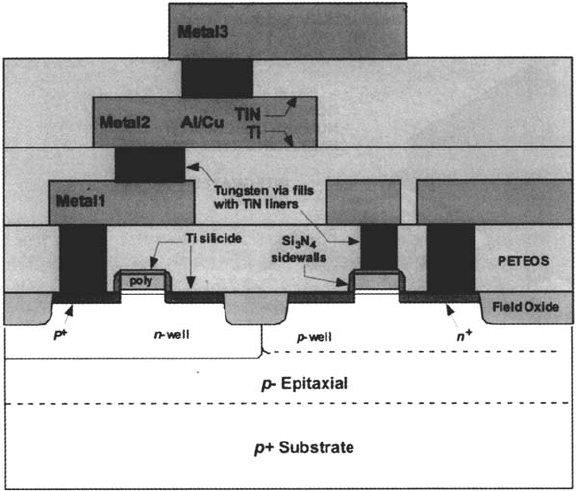
(~100 μm square). A schematic view of these general features and structures is
shown in Figure 1.
The most common materials used for conductors are aluminum-based
alloys, which typically contain small amounts of Si to reduce interdiffusion with
the substrate and Cu to strengthen the metal and limit electromigration. Passivation
layers are often sputter-deposited SiO
2
, chemical-vapor-deposited (CVD) phos-
phosilicate glasses (that provide better coverage), and plasma-deposited silicon
nitride. For corrosion engineers, this passivation layer should not be confused
with the intrinsic oxide layer that protects many engineering alloys. Patterning
of the Al lines is often achieved by subtractive techniques such as wet chemical
etching or reactive ion etching (RIE). Metal selection is sometimes dictated by
processing requirements. For example, tungsten metallization has been used
because it can be deposited by a selective CVD process in which deposition
occurs selectively on metal surfaces. Thus, high-aspect-ratio holes can be filled,
an important consideration as the line widths continue to shrink. Refractory
metals, such as tungsten, are also used as an underlying diffusion barrier. With
the decreasing dimensions of very large scale integration (VLSI) devices, the on-chip
interconnections account for an increasingly large fraction of the total circuit
delay time. As a result, there has been a trend to more conductive metals and
lower dielectric insulators. Recently, IBM pioneered the development and
implementation of technology that permits the use of copper conductors in state-
of-the art IC devices [3].
Corrosion of Data Storage Devices 645
Figure 1 Interconnection structure of typical submicrometer integrated circuit technology
that implements chemical-mechanical polished (CMP) planarized dielectric layers.
Copyright © 2002 Marcel Dekker, Inc.
IC Packaging
Electronic components (e.g., computer mainboard or motor controller) typically use
a multiple-level packaging hierarchy to ensure proper power and signal
distribution among the various discrete devices [1,4,5]. The core, or first level of
packaging, is within the IC itself [6]. Besides permitting electrical communication to
the outside, secondary packaging roles include providing robust mechanical support
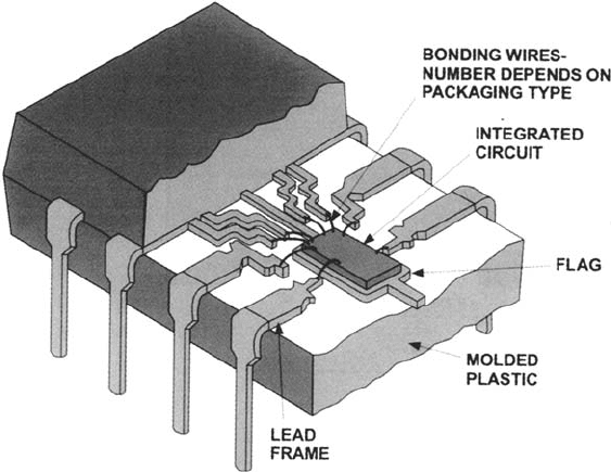
and environmental protection to the chip. Two general types of IC packaging
technology exist: ceramic-hermetic package (CHP) and plastic-encapsulated
microelectronics (PEM). As the terminology implies, CHP devices have ceramic
bodies and the chip enclosure is hermetically sealed, normally by welding, brazing,
or glassing on a metal or ceramic lid. Hence, the chip environment can be tightly
controlled. This technology was dominant 25 years ago and is still preferred by many
for high-reliability applications. With PEM technology, the chip is attached to a metal
support/lead frame fixture and the entire assembly is encapsulated with a plastic
molding compound (Fig. 2 [7]). The molding material is usually a water-permeable
polymer such as epoxy or silicone that is filled with inorganic particles. The
encapsulant material is normally injection molded but can also be cast as a liquid
(glob). Initially, PEM devices were considered unreliable because of corrosion and
encapsulant cracking/delamination issues [8]. However, substantial technological
improvements have been made over the past 20+ years to the point that their reduced
cost, size, and weight; improved reliability; and now high level of availability have
pushed the PEM worldwide market share to over 97% [9]. An excellent detailed
description of the PEM technology and its application is available [9].
The exposed pads on the chip top-level passivation windows are connected
to fingers on the metallic lead frame with fine 25-μm Au or Al wire (Cu or Ag is
646 Frankel and Braithwaite
Figure 2 Sectioned schematic view of a typical plastic-encapsulated integrated circuit.
(From Ref. 7 with permission from General Electric Co. Copyright 1984 by RCA.)
Copyright © 2002 Marcel Dekker, Inc.
sometimes also used) by a solid-state wirebonding process using thermocompression
and/or ultrasonic welding [9,10]. The lead frame, which also forms the external,
board-level interconnects, is usually made from an Ni-Fe alloy, Cu alloy, or Cu-clad
stainless steel. As with discrete connectors, the bare frame is usually given an Ni
or Ni-Co strike and then plated with Au, Ag, or Pd for improved corrosion resistance
and reduced contact resistance [9].
Tape automated bonding (TAB) and controlled collapse chip connection
(C4) are two other common first-level packaging technologies that allow increased
I/O density compared with wirebonding in molded plastic packages. In TAB,
chips are thermocompression bonded to the inside ends of radially patterned metal
leads on polymer tape. The outside ends of the leads are then soldered to a second-
level package and the chip is covered with an encapsulant, so the reliability concerns
are similar to those of PEM devices. In C4 bonding, an array of solder bumps
deposited on a chip is joined to a matching array of pads on the substrate. This
technology, which allows maximum I/O density, has been used primarily in
hermetic high-end applications but is now becoming popular in low-end,
nonhermetic applications.
Macro Interconnects
Functional electrical circuits are formed by interconnecting packaged ICs with
other devices using printed circuit boards (PCB). These boards can be viewed as
second-level packaging. Individual devices are attached to the PCB using some
form of automated or manual soldering process [9]. PbSn alloys are still the
predominant choice for solder, although more environmentally compatible
alternatives are emerging. The conducting lines on PCBs are normally made from
copper and are protected with an Sn or SnPb plating, an organic coating, or an
inorganic passivation layer. Often, a protective, organic-based conformal coating
(e.g., acrylic, polyurethane, epoxy, or silicone based) is applied to the entire board
to ensure cleanliness and reduce direct exposure to the external environment [9].
Low-force, low-voltage separable connectors and contacts also have wide use
in electronic systems [11,12]. A variety of different configurations exist, but the
substrate of most is made from copper, brass, bronze, or copper-beryllium. The use
of copper alloys ensures some susceptibility to environmental degradation. To reduce
interfacial resistance and corrosion, the substrate is plated with a nickel diffusion
barrier and then with a precious metal (e.g., gold, palladium) [11,13]. However, a
trade-off exists between plating cost (thickness) and reliability [14]. Hence, physical
defects (pores and cracks) are usually present. In the past, connectors and contacts
could not be coated because of interference with their function, although some
new coating inhibition formulations have been developed for this purpose [11,12].
Magnetic-Storage Components
All computers, from mainframes to portables, use some form of technology for
long-term data storage and retrieval. This chapter focuses on corrosion in high-
performance magnetic disk storage because this technology is extensively used and
has significant vulnerability to corrosion. The primary material components of a disk
drive are the disk, which has a hard magnetic layer that stores the information, and a
head, which uses a soft magnetic material to write and read the information to and
Corrosion of Data Storage Devices 647
Copyright © 2002 Marcel Dekker, Inc.
from the disk. In obsolete hard drive technology and current low-end devices such
as floppy drives, both heads and disks are made from ceramic materials such as
ferrites and iron oxide, so corrosion is not a concern. In the past 25 years, however,
technological advances in the field of magnetic recording that have driven the
improvements in performance have also introduced metals to both disks and
heads. As a result, the components in disk drives are now susceptible to failure by
corrosion. An excellent review of magnetic-storage technology is contained in the
book my Mee and Daniel [15].
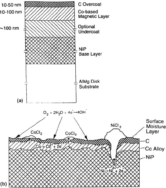
State-of-the-art hard disk drives use thin-film metal disks as a storage medium.
A typical thin-film disk structure is shown in Figure 3a. The magnetic layer is a
Co-based alloy that is on the order of hundreds of angstroms thick and is underneath a
very thin overcoat layer that is often sputtered carbon. This carbon overcoat (COC)
layer as drawn in Figure 3a should be an effective barrier to corrosion because it
physically separates the metallic layers from the environment. In practice, the COC
and thus the disk is also covered with a thin layer of lubricant that can further reduce
corrosion by repelling and/or displacing water. However, Figure 3a is idealistic in
that the layers are not smooth and the carbon overcoat does not completely cover
648 Frankel and Braithwaite
Figure 3 (a) Schematic representation of thin-film disk structure. (b) Schematic view of
corrosion of roughened disk structure in a chloride-contaminated environment.
Copyright © 2002 Marcel Dekker, Inc.
the underlying metallic layers. A more realistic view is given in Figure 3b. The
NiP base layer is intentionally roughened or “textured” to reduce sticking of the
head to the disk when the drive is turned on. The magnitude of this texturing or
roughness can be comparable to the thickness of the COC. As a result, the thin COC
is often unable to cover completely and seal the underlying layers, thereby exposing
susceptible metals to the environment. The corrosion that occurs can result in the
formation of relatively large corrosion product deposits on the disk surface. The
collision of heads with these corrosion deposits on the surfaces of spinning disks can
cause head misalignment and disk failure. Such head “crashes” typically occur in
practice long before the corrosion process causes a significant information error rate.
Several configurations of recording heads are used in disk drives. Thin-film
inductive heads are standard components consisting of miniaturized horseshoe electro-
magnets manufactured by wafer-level fabrication techniques. These devices had been
used for both reading and writing. Now they are used primarily as write elements that
are combined with more sensitive sensors for reading data. The device is imbedded in
an insulator, such as sputtered alumina. It is thus protected from the environment,
except for the two ends of the pole piece (pole tips) and gold bondpads connected to
the coil. The pole piece is often made from electroplated permalloy (Ni-20%Fe) and
the exposed permalloy pole tips are a few μm
2
in area. As in microelectronics, loss of
material from corrosion can have a large influence on such small structures.
The read elements in advanced magnetic heads make use of the magnetoresistance
(MR) phenomenon in which the resistance of a material changes as a function of
magnetic field. The various types of magnetoresistance that are currently used in
magnetic storage devices or under development include, in order of increasing
sensitivity, anisotropic magnetoresistance (AMR), giant magnetoresistance (GMR),
and colossal magnetoresistance (CMR). At the time of this writing, AMR-based
recording heads dominate the market. Enhanced sensitivity devices called spin
valves that utilize GMR will be in full mass production by the year 2000. There
are several designs for the various MR-type sensors that all contain a stack of
numerous thin-film layers, such as Co, Cu, NiFe, and MnFe, each with thickness
on the order of several nm [16]. Most MR sensors use antiferromagnetic layers to
pin the domains of adjacent soft magnetic layers by exchange coupling, although
many AMR devices use a hard magnetic layer instead. MnFe, containing about
50% of each element, is a commonly used antiferromagnetic layer and is extremely
corrodible. To be used in a disk drive, a cross section of the thin films in the sensor
must be exposed at the device surface. This is achieved by abrasive lapping in an
aqueous environment. Lapping is potentially very aggressive because fresh metal
area is continually exposed to the aqueous lapping environment. Like disks, MR
heads are often covered with a thin carbon overcoat after lapping, and this COC
provides corrosion protection once it is in place.
Magneto-optic (MO) recording is another type of data-storage technology that
is not as widely used as magnetic storage but poses special corrosion concerns. MO
disks are erasable and have very high bit density. Because the disks are removable
and thus handled by users, they are exposed to an uncontrolled range of conditions.
The active layer in some MO drives is composed of a rare earth–transition metal
alloy such as Fe-25Tb and is several hundred angstroms thick. The high Tb content
makes these alloys extremely reactive. The MO film is deposited onto glass substrates
Corrosion of Data Storage Devices 649
Copyright © 2002 Marcel Dekker, Inc.
and then covered with a thin oxide layer and a thin metallic layer as such as Al.
Two such substrates sealed back to back with epoxy constitute an MO disk.
Moisture can penetrate through the permeable epoxy and cause corrosion of the Al
layer or of the MO layer where it is exposed.
MICROELECTRONIC CORROSION
Because corrosion has been and continues to be one of the prime degradation modes
observed in microelectronic devices, a significant number of in-depth corrosion
studies have been performed during the past two decades and several noteworthy
review articles have been written [7,17–23]. For reference and to be consistent with
the terminology used in the electronics community, corrosion is defined as the
degradation of metallic features resulting from interactions with environments
containing water or moisture. An important consideration to remember when
assessing some of the historical information that follows is that the microelectronic
technology has improved substantially over the years. Many of the early concerns
and problems are no longer relevant to modern microelectronics. Also, because
microelectronic devices are exposed to atmospheric conditions only during use, much
of our existing knowledge of atmospheric corrosion is applicable. This subject is
addressed by Leygraf in Chapter 15 of this book. Leygraf and Graedel [24]
have written a textbook on atmospheric corrosion. An additional reference is the
comprehensive review of this subject was that was compiled by Ailor [25] and
contains information on fundamental aspects, behavior of specific metal systems,
and testing.
Environmental Factors
Regardless of the type of device or the offending corrosion mechanism, corrosion-
induced degradation involves interactions with the environment. The critical factors
that must always exist are a susceptible metallization, the presence of moisture, and
some type of contaminating ionic species. This subsection describes some of the
aspects of the latter two factors common to corrosion of all microelectronic devices.
Water Adsorption
Under noncondensing atmospheric conditions, water adsorbs on metal and metal-oxide
surfaces and forms a thin layer. The thickness of the layer ranges from < 1 to tens
of monolayers and depends primarily on the relative humidity (RH) and the substrate
material [26,27]. At 20% RH, approximately one monolayer exists on average,
whereas at 75% RH, the thickness increases to about five monolayers. Often the
water layers cluster and so local thicknesses are probably greater. The corrosion rate
for most metals is a function of the thickness of the adsorbed water layer and
therefore the RH. Usually, the corrosion rate as a function of RH has a sigmoid-
shaped response. The critical humidity level above which the corrosion rate
significantly accelerates (lower inflection point in sigmoidal curve) ranges from 15 to
90% RH but is typically > 50% and is thought to be the RH at which at least three
monolayers of water exist. In general, if the humidity is lower than the critical level,
the corrosion rate is minimal and the reaction process is essentially dry (requiring
a direct gas-metal ambient-temperature interaction). Above this critical level, the
650 Frankel and Braithwaite
Copyright © 2002 Marcel Dekker, Inc.
adsorbed water phase becomes “quasi-aqueous” and is thus capable of supporting
faster electrochemical charge transfer reactions. The final important water-
adsorption aspect is associated with the extremely small physical features found
in microelectronics where capillary condensation can occur. Examples include
under the lip of a wirebond, between connector surfaces, and in defects in the
plastic encapsulant. This condensation phenomenon can produce very bulk-like
localized aqueous conditions at humidity levels 100%. A more in-depth description
of water adsorption is presented in the chapter on atmospheric corrosion.
The temperature of the device can have a dramatic effect on water adsorption.
For a given absolute humidity level, higher surface temperatures result in desorption
of water (localized decrease in relative humidity according to the psychrometric law).
As noted in the previous paragraph, an associated decrease in the corrosion rate could
be produced. For many ICs, these higher temperatures occur when their power is on
because of internal ohmic heating. Besides surface desorption, water is also driven
out of the package. Ajiki et al. [28] did a benchmark study in 1979 that is still
relevant today. They showed that device reliability increases with increasing power
dissipation and with an increasing ratio of time on to time off. This correlation is
simply due to moisture effects and a related worst-case condition could then be
long-term dormant storage [29].
Contamination
Introduction of corrosive contaminants that may result in long-term reliability
concerns can occur during manufacturing and/or use. Many of the fabrication process
steps involve exposure to aggressive species and can leave corrosive residues. For
example, reactive-ion etching (RIE) of Al metallization is performed in plasmas
containing combinations of gases such as Cl
2
, CCl
4
, CHCl
3
, and BCl
3
[30–36]. If
removed untreated from the etcher, patterned structures are covered with high levels
of AlCl
3
, which is hygroscopic and can later form HCl in the presence of moisture.
The sidewalls of the patterned photoresist that is used to mask areas that are not to be
etched can also retain large amounts of chloride contamination. Other typically
benign process solutions, such as deionized (DI) water and organic solvent rinses, can
become contaminated over time from process chemical residues [37,38].
In addition, airborne particles or particles that are too small to be filtered out
by the best clean room facilities can be deposited on susceptible surfaces. Studies
performed at AT&T Bell Laboratories have highlighted the potential role of airborne
particles in the corrosion of electronic devices that are relevant to both manufacturing
and actual use conditions [20,39,40]. Sinclair [20] has shown that there exist in the
environment a large number of fine particles (with aerodynamic diameters of
0.05–2 μm) that are rich in ammonium acid sulfate, derived from anthropogenic
sources, and difficult to remove by filtration. Ionic compounds, such as these,
often deliquesce above a certain RH level [41,42]. Another significant contaminant
that can be introduced during manufacturing is solder flux/residue that may not be
completely removed or reacted during PCB soldering operations [43]. Some
materials in the microelectronics themselves can be a source of undesired chemical
species. For example, plastic epoxy encapsulants can contain a fire-retarding
agent that includes an organic bromine compound. Phosphorus is a component
in many of the passivation glasses. With time, interaction and leaching with
Corrosion of Data Storage Devices 651
Copyright © 2002 Marcel Dekker, Inc.
adsorbed moisture can produce corrosive species such as bromide salts or phosphoric
acid [10,17].
Leygraf, in the chapter on atmospheric corrosion, discusses the environmental
differences between indoor and outdoor exposure conditions and why these
differences are important to corrosion of electronics. Although the service
environments for electronic devices are typically less severe than for many other
types of equipment, industrial atmospheres do contain harmful oxidizing (e.g., Cl
2
,
SO
2
, NO
x
) and halide-containing (e.g., NaCl) species that can diffuse or migrate to
microelectronic metallization, especially over an extended service life. Because of the
importance of contamination control, techniques to quantify microscopic levels on
have been developed [30,44].
Mechanisms
Because of the wide range of possible environments and the large number of
metallic materials used in microelectronic devices, corrosion occurs by a number
of different physical mechanisms that can be grouped into two general categories:
those driven by the application of an applied potential (under electrical bias) and
those occurring under static (open-circuit) conditions.
Under Electrical Bias
Although the potential that is applied to microelectronic devices is normally
relatively limited (< 5V), very large electric fields can result because of the very
small separation distances between conductors. When condensed water and ionic
contamination are present between the lines (on the surface of separating insulators),
these fields produce undesirable results by means of the three separate, but related
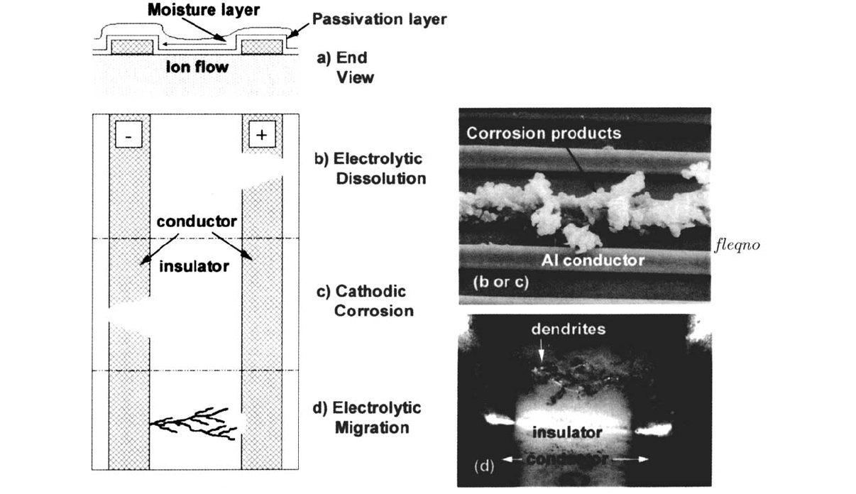
mechanisms described next and shown schematically in Figure 4. For reference, these
processes are often referred to as electrolytic. An extensive review of this subject
was compiled by Steppan et al. [45]. The voltage driver is normally externally
applied, but another source is the semiconductor junctions that exist within an IC
[17]. Most environmentally induced failures in ICs that are observed in practice, and
especially during accelerated aging, are caused by the applied electrical bias.
If an ionic path is present between two oppositely biased metal lines that are
otherwise isolated and the path resistance is adequately low, then sufficient voltage
will exist to enable an electrical current to flow between the lines (Fig. 4a). A
portion of the applied voltage difference will exist at each metal-electrolyte
interface, permitting electrochemical oxidation/reduction reactions to occur. The
extent of the resulting corrosion depends on many factors, but the resistance of the
ionic pathway is the most important. The influence of increasing moisture and con-
tamination on decreasing the ohmic resistance of the ionic path is further explained
by Osenbach [17] and has been phenomenologically modeled by Comizzoli [46].
Contamination has a further role because of its effect on the breakdown of the
passive oxide on many metals.
Electrolytic Dissolution In this mechanism, the current leak results in
electrochemical oxidation of the positive, anodic conductor. Eventually, the
device can fail from an open circuit in the anodic line (Fig. 4b). Given the small
dimensions and volume of the adsorbed electrolyte, severe concentration gradients
exist and voluminous corrosion products can precipitate near the surface [e.g.,
652 Frankel and Braithwaite
Copyright © 2002 Marcel Dekker, Inc.
Corrosion of Data Storage Devices 653
Figure 4 Schematic diagram of the effect of the three primary corrosion mechanisms that occur in integrated circuits due to the presence of mois-
ture and an applied electrical bias. The photograph in the upper right is a typical result of either electrolytic dissolution or cathodic corrosion (depends
on location of defects in the passivation layer). The lower right photograph shows a short-producing electrolytic migration of solder that occurred in a
ceramic capacitor in the presence of high humidity and a chloride-containing flux residue.
Copyright © 2002 Marcel Dekker, Inc.