Alkauskas A., Deak P., Neugebauer J., Pasquarello A., Van de Walle Ch.G. (Eds.) Advanced Calculations for Defects in Materials: Electronic Structure Methods
Подождите немного. Документ загружается.

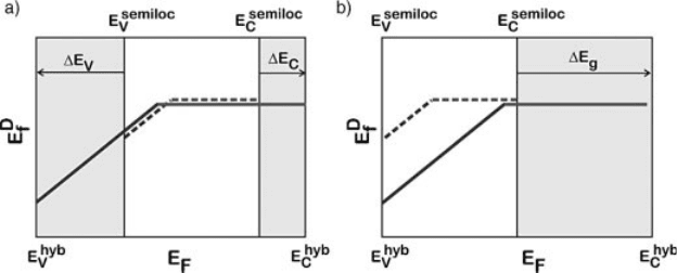
(solid lines) functional. The formation energy of a positively charged defect has a
positive slope, while that of a neutral defect has a zero slope. The charge transition
level corresponds to the value of the electron chemical potential at which the two
charge states have equal formation energies. In Figure 7.6a, the transition levels in
the two approaches are aligned with respect to the average electrostatic potential as
discussed in Section 7.3.1. Let us assume that for the specific defect in Figure 7.6 the
charge transition levels in the two theories are indeed very close when referred to
the average electrostatic potential. The formation energy of the neutral defect does
not depend on the electron chemical potential and we here additionally assume that
this energy is quite similar when calculated with semilocal and hybrid functionals.
Consequently, this also implies that the formation energies of the positively charged
defect are also similar in the two calculations, provided they are taken at the same
value of the electron chemical potential referred to the average electrostatic potential.
However, since the position of the VBM is different in the two theoretical approaches,
the formation energies of the positively charged defect are different when the
electron chemical potential is referred to the respective VBM. Thus this clearly
illustrates that when the electron chemical potential is found at the VBM as, e.g., for
a p-type material, the formation energy of the positively charge defect depends on
the location of the VBM relative to the average electrostatic potential. The position of
band edges with respect to the average electrostatic potential will be discussed in the
next section.
For comparison, we also discuss an alternative alignment scheme which has often
been adopted in the literature and which consists in aligning the VBM in the two
theoretical approaches, as schematically shown in Figure 7.6b. This alignment
scheme assumes that the band-gap problem originates from the wrong placement
of the CBM. With this alignment, the charge transition levels are no longer aligned,
Figure 7.6 (online color at: www.pss-b.com)
Formation energies of a point defect as a
function of the electron chemical potential E
F
calculated with a semilocal (dashed lines) and
with a hybrid functional (solid lines). The
positive and neutral charge states of the defect
are considered. (a) The semilocal and the hybrid
calculations are aligned through the average
electrostatic potential as in Fig. 7.4; DE
V
and
DE
C
are the corresponding shifts in the VBM
and in the CBM. (b) The VBM of the two
calculations are aligned; DE
g
is the band-gap
underestimation in the semilocal calculation
with respect to the hybrid one.
7.3 General Results from Hybrid Functional Calculations
j
123
and the formation energies of the positively charged defect differ for any value of the
electron chemical potential. Under the assumption that the VBM are aligned, it
appears contradictory that two theoretical approaches that bear similar total energies
for the neutral state would instead differ systematically for the positive charge state,
especially when such a charge state results from the absence of electrons in the defect
state.
7.3.4
The Band-Edge Problem
In this section, we elaborate on the band-gap problem in relation with the
determination of defect levels and argue that it is more appropriate to refer to
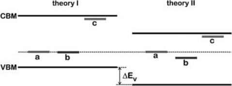
a band-edge problem. For this purpose, let us consider two different theories, I and
II, which both yield a theoretical band gap in agreement with the experimental one,
but different positions of band edges when referred to the average electrostatic
potential, as schematically shown in Figure 7.7. For illustration, we consider three
kinds of defects. The defect of kind (a) corresponds to an atomically localized defect,
for which the energy level does not undergo a significant shift, in accord with our
observations in Section 7.3.2. On the other extreme, defect (c) corresponds to
a shallow hydrogenic-like impurity which is known to shift with the band edge to
which it is tied. We also consider a defect level (b) of intermediate extension, which
follows the band edges only to a limited extent.
Figure 7.7 clearly illustrates that reproducing the correct band gap is not
a sufficient condition to achieve a correct description of defect levels. When calculated
defect levels are compared with experimental ones, the VBM and CBM are natural
reference levels. Indeed, the charge transition levels of defects (a) and (b) referred to
their respective theoretical VBM are different despite the fact that the two theories
correctly reproduce the experimental band gap! This is a direct consequence of the
analysis in Section 7.3.2. For the specific case of the oxygen vacancy in ZnO, such
considerations explain to a large extent the scatter of calculated charge transition
Figure 7.7 (online color at: www.pss-b.com)
The band-edge problem. Comparison of two
electronic structure methods, theory I and
theory II, for calculations of energy levels of
different types of defects: (a) an atomically
localized defect; (b) a defect of intermediate
extension; (c) a shallow hydrogenic-like
defect. The two theories yield the same
band gap but different absolute positions
of the band edges when referred to the
average electrostatic potential. Adapted
from Ref. [65].
124
j
7 Defect Levels Through Hybrid Density Functionals: Insights and Applications

levels found in the literature [65]. Indeed, different band-gap correction schemes lead
to different band-edge positions, while the defect level is generally well defined when
referred to the average electrostatic potential [65].
7.4
Hybrid Functionals with Empirically Adjusted Parameters
The comparison of defect charge transition levels calculated with semilocal and
hybrid functionals provides insight into the way energy levels of deep defects shift as
the description of the band gap improves. The analysis suggests that such defect
levels are generally well described at the semilocal level when referred to the average
electrostatic potential. Hence, the positioning of the defect levels within the band gap
mainly depends on the accuracy by which the adopted functional determines the
band edges with respect to this alignment scheme.
As stressed above, a hybrid functional scheme based on the use of a fixed mixing
coefficient a does not always yield band gaps in good agreement with experiment.
In this section, we address the issue whether band edges determined by hybrid
functionals are accurately positioned with respect to the average electrostatic poten-
tial, when the mixing coefficient a is tuned to reproduce the experimental band gap.
While such an empirical approach is currently in use in the literature, it is ultimately
not satisfactory and higher levels of theory will be required to improve the description
of the band edges. Nevertheless, the band-gap tuning approach offers a practical
scheme in which defect levels are positioned within a band gap of the right value
and which can completely be treated within a hybrid functional formulation. It is
also based on the well-documented assumption that the structural parameters are
generally only moderately affected when the mixing coefficient varies [16, 40, 79],
unless the electronic structure itself undergoes important modifications.
As shown in Figure 7.8 for a selected set of materials, semilocal functionals
systematically underestimate the experimental band gap. Hybrid functionals gen-
erally yield band gaps increasing linearly with the mixing coefficient a [68]. Hence, an
optimal mixing coefficient can generally be found for any material:
a
opt
¼
E
expt
g
E
semiloc
g
k
; ð7:8Þ
where k ¼ dE
g
=da is the derivative of the band gap with respect to the mixing
coefficient. The linear dependence results from the fact that the electron wave
functions associated to the band edges do not change significantly with a. Further-
more, this property also signifies that the nature of the band edge states does not
change. Indeed, the energy levels of different bands generally behave differently as
a varies. Thus, a departure from linearity is expected when the character of the VBM
or the CBM changes, as might occur, for example, when sp and d bands cross.
We can provide some support for the tuning of the parameter a by invoking the
reasoning of Gygi and Baldereschi [80] in their construction of an approximate GW
scheme. Let us consider the nonlocal exchange–correlation potential provided by the
7.4 Hybrid Functionals with Empirically Adjusted Parameters
j
125
hybrid density functional as a certain approximation to the many-electron exchan-
ge–correlation self-energy in the GW approximation, and more particularly to its
frequency-independent form, the COHSEX approximation. In this approximation,
the long-range interaction is described by screened exchange (SEX), which asymp-
totically approaches 1=e
1
ðjrr
0
jÞ. In the hybrid functional formulation, the
semilocal part of the exchange–correlation is short-ranged [81] and the long-range
part is therefore entirely described by the fraction a of exact exchange: a=jrr
0
j. The
assumption that the hybrid functional correctly describes the long-range limit, gives
the following relation for the optimal mixing coefficient:
a
opt
1
e
1
: ð7:9Þ
For metals e
1
¼1, and thus a
opt
¼ 0, which is a correct and intuitive result. In
a metal any fraction of exact exchange would produce unphysical derivative dis-
continuities (e.g., qe
k
=qk) at the Fermi level. The present discussion is also fully
consistent with the reasoning of Fiorentini and Baldereschi [82], who showed that the
error in the semilocal band gap approximately scales like 1=e
1
. Indeed, the smaller
the difference between the semilocal and the experimental band gap, the larger the
required fraction a
opt
of exact exchange in the optimal hybrid functional.
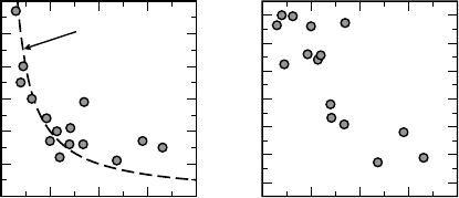
In Figure 7.9a, we show the optimal mixing coefficient a
opt
versus e
1
for various
materials. Despite some scatter, a clear correlation between a
opt
and 1=e
1
is indeed
apparent. The most evident out-liers, Ge, GaAs, and ZnO, all possess semicore 3d
states. This suggests that the long-range screening is not the only property affecting
the band gap, and that there is also an effect associated to the s–d coupling [84], which
cannot be captured by tuning a to 1=e
1
. Other reasons for the data scatter are that
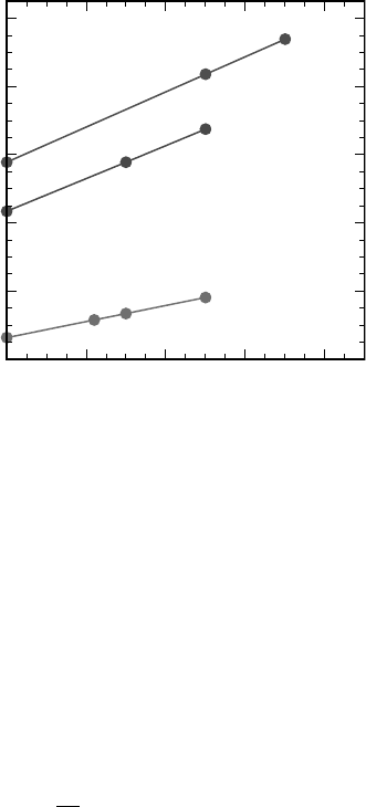
0 0.1 0.2 0.3 0.4
a
0
2
4
6
8
10
E
g
(eV)
Si
HfO
2
SiO
2
Figure 7.8 (online color at: www.pss-b.com) Dependence of the theoretical band gap on the mixing
coefficient a (Eq. 7.5) for several materials. For each material, there is an optimal mixing coefficient
a
opt
for which the hybrid functional reproduces the experimental band gap.
126
j
7 Defect Levels Through Hybrid Density Functionals: Insights and Applications
hybrid functionals with a
opt
¼ 1=e
1
might inappropriately describe the short-range
limit, completely lack the frequency-dependence of the many-body self-energy, and
do not account for the anisotropy of the long-range screening when present.
Nevertheless, the correlation in Figure 7.9 suggests that the dominant physics is
given by the long-range exchange behavior. This is further supported by the good
correlation with e
1
shown in Figure 7.9b for the quantity k ¼ dE
g
=da, i.e., the
derivative of the band gap with respect to the mixing coefficient. The latter quantity
essentially corresponds to E
HF
g
E
semiloc
g
, i.e., the difference between the band gap
calculated in the Hartree–Fock and in the semilocal scheme.
Once the band gap is tuned to the experimental one, the hybrid functional scheme
also provides the shifts of the valence and conduction bands, DE
V
and DE
C
. These
shifts result from the alignment of the semilocal and hybrid schemes through the
average electrostatic potential (cf. Section 7.3.1). They indicate to what extent
the conduction and valence bands contribute to the band-gap opening. In a hybrid
functional formulation, their relative contributions solely depend on the effect of the
nonlocal exact exchange operator. The values of these shifts are critical for a correct
placement of defect levels within the band gap. The issue that concerns us here is to
what extent exact exchange is reliable for the evaluation of such shifts.
In principal, the accuracy of calculated band-edge shifts can be assessed through
the consideration of surface systems. Given a well-defined surface structure, the
ionization potential and the electron affinity with respect to the vacuum level could be
calculated. However, photoemission data for semiconductor and insulator surfaces
might be affected by charging effects and by the occurrence of defects and impurities
influencing the electrostatics. Therefore, we here prefer to consider band offsets at
semiconductor–oxide interfaces, where such electrostatic effects appear better
controlled. For a specific interface system, the band offsets can be achieved through
the method of Van de Walle and Martin [67]. The band offsets in the hybrid functional
scheme can be derived from those in the semilocal scheme through the consideration
of the variation of the electrostatic potential offset and through the application of the
20151050
ε
∞
0.0
0.1
0.2
0.3
0.4
0.5
a
opt
20151050
ε
∞
4
5
6
7
8
9
10
dE
g
/da
1/ε
∞
b)a)
Figure 7.9 (online color at: www.pss-b.com)
(a) Optimal mixing coefficients a
opt
and (b) the
derivative of the band gap k ¼ dE
g
=da versus
the dielectric constant e
1
for various
materials. The data for the band gaps are
taken from the results in Fig. 7.1 and a
linear dependence of the band gap on the
mixing coefficient a is assumed. For e
1
,
we used experimental data from
Ref. [83].
7.4 Hybrid Functionals with Empirically Adjusted Parameters
j
127

shifts DE
V
and DE
C
[68, 85]. On either side of the interface, the theoretical band-gap
matches the experimental one by construction. Such a scheme generally requires the
use of different a
opt
for the two bulk components of the interface and is applicable
owing to the weak dependence of the interfacial dipole on the mixing parameter
a [68]. The comparison between calculated and measured band offsets then provides
a sensitive test for the accuracy of band edges as obtained in hybrid functional
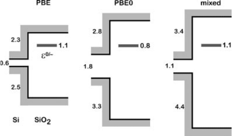
schemes. In Table 7.1, we present band offsets calculated for three interface model
systems: Si/SiO
2
(Refs. [86, 87]), SiC/SiO
2
(Ref. [88]), and Si/HfO
2
(Ref. [28]). When
the hybrid functionals are tuned to match the experimental band gaps of the two
interface components (cf. mixed in Table 7.1), the calculated band offsets are found
to agree with experiment within only 0.1 eV [89–91]. Despite the limited number of
studied systems, the good agreement in Table 7.1 is very encouraging and suggests
that hybrid functionals may be relied upon for positioning band edges. This would
also imply that nonlocal exchange is the primary cause determining the relative size
of band-edge shifts.
Another way of validating the shifts of the band edges obtained from the hybrid
functional calculation is through comparison with those calculated with a theory of
higher level, such as for instance the GW many-body perturbation theory. Recently,
Shaltaf et al. [92] performed GW calculations focusing on such shifts. In Table 7.2, we
compare shifts in band edges as obtained with a hybrid functional with those
obtained by Shaltaf et al. [92] for Si and SiO
2
. The band gaps in the hybrid functional
calculations with a tuned mixing coefficient are by construction exactly equal to the
experimental ones, whereas this is not necessarily the case for the various GW
approaches. It is therefore more useful to compare relative shifts in the valence and
conduction band, i.e., DE
V
=DE
g
and DE
C
=DE
g
as obtained in various theoretical
schemes. One observes that results obtained with the hybrid functional and with the
various GW schemes differ by approximately the same amount as the various GW
schemes differ among themselves. This suggests that the quality of the VBM and
CBM shifts provided by the hybrid functional scheme is comparable to that achieved
with GW methods.
It should be stressed that the study of Shaltaf et al. [92] also showed that in GW
schemes these shifts are more difficult to converge than the band gap, requiring
Table 7.1 Valence (DE
V
) and conduction (DE
C
) band offsets at the Si/SiO
2
, SiC/SiO
2
, and Si/HfO
2
interfaces calculated in PBE, PBE0, and the mixed scheme (Ref. [68]), in which the mixing coefficient
a is different for the two interface components. Experimental band offsets are from Refs. [89, 90] and
[91], respectively.
interface PBE PBE0 mixed expt.
Si/SiO
2
DE
v
2.5 3.3 4.4 4.4
DE
c
2.3 2.7 3.4 3.4
SiC/SiO
2
DE
v
1.4 2.0 3.0 2.9
DE
c
1.7 2.0 2.6 2.7
Si/HfO
2
DE
v
2.3 3.1 2.9 2.9
DE
c
1.5 1.9 1.7 1.7
128
j
7 Defect Levels Through Hybrid Density Functionals: Insights and Applications

a very high number of empty states in the calculation of the response functions.
Furthermore, these shifts are sensitive to various ingredients of the calculation, such
as the plasmon pole approximation, the level of self-consistency of the GW approx-
imation, and the vertex corrections [92]. These considerations limit the amount of
materials for which such shifts have hitherto been obtained in a reliable way at the
GW level.
7.5
Representative Case Studies
In this section, we illustrate the application of hybrid functionals to the study of
defects through two case studies.
7.5.1
Si Dangling Bond
The first case study concerns the Si dangling bond. This defect corresponds to the
atomic structure of the P
b
center, which has clearly been observed at interfaces
between silicon and its oxide [93]. The dangling bond was modeled by removing four
neighboring atoms in a bulk supercell of 216 silicon atoms [29]. Nine of the ten
dangling bonds generated in this way were then passivated with H atoms. The core
structure of the model is identical to that used in Ref. [23] for modeling the Ge
dangling bond.
The relevant charge states of the dangling bond are the positive, the neutral, and
the negative charge states. Charge transition levels were calculated in the PBE (the
mixing coefficient a ¼ 0), the PBE0 (a ¼ 0:25), and with a hybrid functional defined
by an intermediate mixing coefficient a ¼ 0:10. The evolution of the charge tran-
sition levels as well as that of the band edges are shown in Figure 7.10a as function
of a [29]. The band structures are aligned through the average electrostatic potential.
All displayed levels shift linearly with a. The largest shifts are observed for the band
edges. The shifts of the charge transition levels e
þ= 0
and e
0=
are more moderate,
in agreement with general findings [13]. The charge transition levels reported in
Table 7.2 Relative shifts of the valence band (DE
V
) and the conduction band DE
C
with respect to
the change in the band gap DE
g
for Si and SiO
2
, as determined with a hybrid functional (PBE0),
a GW, and a quasiparticle self-consistent GW (QS GW) scheme. The latter two results are taken from
Ref. [92].
material quantity hybrid GW QS GW
Si DE
V
=DE
g
0.54 0.67 0.75
DE
C
=DE
g
0.46 0.33 0.25
SiO
2
DE
V
=DE
g
0.69 0.56 0.68
DE
C
=DE
g
0.31 0.44 0.32
7.5 Representative Case Studies
j
129
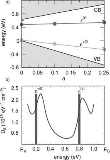
Figure 7.10a include the electrostatic Makov–Payne correction. For the present
supercell calculation, the application of this correction yields converged values for
the charge transition levels [29].
A hybrid functional calculation with a mixing coefficient a ¼ 0:11 precisely
reproduces the experimental value of the Si band gap, E
g
¼ 1:17 eV. For this value
of a, we obtained charge transition levels at e
þ=0
¼ E
V
þ0:2 eV and e
0=
¼ E
V
þ0:8
eV. We compare these values in Figure 7.10b to the experimental density of interfacial
traps at the Si–SiO
2
interface as obtained from C=V measurements [93]. The
calculated charge transition levels are found to closely correspond to the two
experimental peaks at E
V
þ0:26 eV and E
V
þ0:84 eV, generally assigned to Si
dangling bonds. The good agreement in Figure 7.10b provides support to the practice
Figure 7.10 (online color at: www.pss-b.com)
(a) Dependence of Si band edges and of the
charge transition levels e
þ=0
and e
0=
of the Si
dangling bond defect on the mixing coefficient
a. The vertical energy scale is referred to the
VBM in the PBE calculation. Adapted
from Ref. [29]. (b) Density of interfacial
traps at the Si–SiO
2
as measured by the
low-frequency C=V technique in Ref. [93] (solid
line). The two pronounced peaks at 0.26 and
0.84 eV originate from P
b
defects and
correspond to the charge transition levels e
þ=0
and e
0=
. The charge transition levels
obtained through a hybrid functional
calculation with a ¼ 0:11 are represented
by vertical bars.
130
j
7 Defect Levels Through Hybrid Density Functionals: Insights and Applications
of using a mixing coefficient a that brings the theoretical band gap obtained within
the hybrid functional scheme in accord with the experimental one.
7.5.2
Charge State of O
2
During Silicon Oxidation
The second case study concerns the charge state of the O
2
molecule during silicon
oxidation. The silicon oxidation process has attracted considerable interest because of
its key role in the manufacturing of Si-based microelectronic devices. Our present
understanding relies to a large extent on the oxidation model proposed by Deal and
Grove [94]. In this model, the growth of SiO
2
proceeds by (i) the adsorption of the O
2
molecule on the oxide surface, (ii) the diffusion of molecular O
2
through the bulk-like
oxide, and (iii) its subsequent reaction at the semiconductor–oxide interface. Sim-
ulation techniques based on DFT have been instrumental for achieving an atomic-
scale description of the involved processes [95], such as, e.g., the diffusion mech-
anism of O
2
in amorphous SiO
2
[96], the oxidation reaction [97], etc. However, one
aspect that has long been difficult to address is the charge state of the diffusing oxygen
molecule. The difficulty of providing a clear answer to this issue stems from the
band-gap problem of semilocal approximations to DFT [30, 98].
In bulk SiO
2
, the oxygen molecule is stable in the neutral and in the negative charge
states [96]. The charge state of the O
2
in the vicinity of the Si/SiO
2
interface is
determined by the position of the ð0=Þcharge transition level with respect to silicon
band edges. It is assumed that the molecule is close enough to the interface to allow
for charge equilibration with the silicon substrate, yet remaining far from the
suboxide region where the oxidation reaction takes place. Thus, the ð0=Þ charge
transition level of the O
2
molecule is first determined in a bulk-like amorphous SiO
2
environment and then positioned with respect to Si band edges through the band
alignment at the Si/SiO
2
interface. In Figure 7.11, we show the result of such an
alignment procedure as obtained within three different theoretical schemes [30]:
(i) the semilocal (PBE) functional; (ii) the hybrid (PBE0) functional; (iii) a mixed
scheme, in which the fractionof exactexchange is tuned for each interface component,
following the prescription for the calculation of band offsets given above [68].
All three theoretical schemes consistently indicate that the ð0=Þcharge transition
level locates above the Si CBM (Figure 7.11), providing convincing evidence that for
electron chemical potentials in the Si band gap the neutral charge state is thermo-
dynamically favored. The three schemes show only small quantitative differences.
The separation between the ð0=Þcharge transition level and the Si CBM is 1.1 eV in
the PBE and in the mixed scheme, and reduces to 0.8 eV in the PBE0.
To obtain such a level of qualitative agreement between different theoretical
schemes, charge transition levels and band offsets were obtained consistently within
each scheme. This should be contrasted with the practice of determining transition
levels with respect to the oxide band edges within PBE and using the experimental
band offsets for alignment with respect to the Si band edges. Such an alignment
procedure implicitly takes the erroneous assumption [68, 92] that the band-gap
correction is achieved by the sole displacement of the conduction band. In the case of
7.5 Representative Case Studies
j
131
the O
2
molecule in SiO
2
, this approach results in the opposite conclusion that it is the
negative charge state which is thermodynamically favored [98].
7.6
Conclusion
Our investigation indicates that hybrid functional schemes offer a viable theoretical
tool for determining the location of energy levels of deep defects with respect to the
band edges of the bulk material. The issue is conveniently addressed by separately
aligning the defect level and the band edges with respect to the average electrostatic
potential. In this way, the determination of the defect level can to a large extent be
decoupled from the determination of bulk band edges.
As far as the defects are concerned, it appears that their energy levels with respect to
the average electrostatic potential are already well described at the semilocal level and
that the hybrid-functional description does not lead to any significant modification.
In the case of ionization potentials of molecular systems, a similar agreement is
recorded and the comparison with experiment shows that an accurate description is
achieved. In analogy with the molecular case, this therefore suggests that the energy
separation between the defect level and the average electrostatic potential is in many
cases already accurately determined at the semilocal and hybrid functional level.
At variance, the position of the band edges is highly sensitive to the fraction of
exact exchange considered in the hybrid functional calculation. The use of any fixed
fraction of exact exchange does not lead to a systematic improvement of the band-gap
description, thereby hindering the use of a hybrid-functional scheme as a predictive
tool. It is therefore necessary to resort to an electronic structure method of higher
accuracy to identify the position of the band edges. It should be noted that such
Figure 7.11 (online color at: www.pss-b.com)
The alignment of the ð0=Þ charge transition
level of the O
2
molecule at the Si/SiO
2
interface
is obtained within three different theoretical
schemes: a semilocal functional (PBE), a hybrid
functional (PBE0), and the mixed
scheme. The Si band gap, the Si/SiO
2
band
offsets, and the separation between the
defect level and the silicon CBM are given
in eV. From Ref. [30].
132
j
7 Defect Levels Through Hybrid Density Functionals: Insights and Applications