Alkauskas A., Deak P., Neugebauer J., Pasquarello A., Van de Walle Ch.G. (Eds.) Advanced Calculations for Defects in Materials: Electronic Structure Methods
Подождите немного. Документ загружается.


ionic cores are described with soft norm-conserving pseudopotentials [44]. Through-
out this study, we used a kinetic energy cutoff of 70 Ry, sufficiently high to converge
the properties of all the pseudopotentials in this work, including Hf, O, and C. As
reference GGA functional, we adopted the functional proposed by Perdew, Burke,
and Ernzerhof (PBE) [45]. Pseudopotentials were generated at the PBE level and were
used unmodified in calculations with hybrid functionals. Although this is not
formally justified, this approach gives a very good description for systems with
first-row elements, as can be inferred from comparisons with all-electron calcula-
tions [46]. However, for heavier elements this approximation may admittedly involve
errors [47]. The Brillouin zone was sampled at the sole C-point in most calculations,
but denser k-point meshes were used when necessary, for example in the determi-
nation of accurate band-edge shifts. Further technical details about specifi c systems
are given below. Structural relaxations were carried out at the PBE level. We used the
codes CPMD [48, 49] and Quantum-ESPRESSO [50].
7.2.1
Defect Formation Energies and Charge Transition Levels
The principal quantity that needs to be calculated is the formation energy E
D;q
f
of the
defect D in its charge state q as a function of the electron chemical potential E
F
[51]:
E
D;q
f
ðE
F
Þ¼E
D;q
tot
E
bulk
tot
X
a
n
a
m
a
þqðE
V
þE
F
Þ: ð7:1Þ
In this expression E
D;q
tot
is the total energy of the defect system, E
bulk
tot
the total energy of
the unperturbed host, n
a
the number of extra atoms of species a needed to create the
defect D, and m
a
is the corresponding atomic chemical potential. The electron
chemical potential is referred to the valence band maximum (VBM) E
V
. It varies
between zero and the band-gap E
g
. Charge transition levels correspond to specific
values of the electron chemical potential for which two charge states have equal
formation energies. Let us for example consider charge states q and q
0
. Equating the
expressions of the formation energies defined in Eq. (7.1);, we obtain the value for the
charge transition level eðq=q
0
Þ:
eðq=q
0
Þ¼
E
D;q
tot
E
D;q
0
tot
q
0
q
E
V
: ð7:2Þ
For example, the charge transition level eð0= þÞ is given via:
eð0= þÞ¼E
D;0
tot
E
D; þ
tot
E
V
: ð7:3Þ
The total energies of charged systems appearing in Eq. (7.1) need to be corrected to
speed up the convergence with respect to the supercell size. First, the total energy is
corrected by a term qDV, DV being the potential difference needed to align the
potential far from the neutral defect to that of the unperturbed bulk. Second, the total
energy is corrected for the spurious electrostatic interaction due to the periodic
boundary conditions, for which we use the electrostatic correction of Makov and
7.2 Computational Toolbox
j
113

Payne [52]. These two corrections are always used unless otherwise stated. While the
Makov–Payne correction is known to fail in some specific cases, it is generally
quite accurate in the case of extremely localized defects. For instance, for defects in
SiO
2
, the charge transition levels are already converged for moderate supercell
sizes (72 atoms) when this electrostatic correction is included. When accurate quan-
titative results are needed, it is recommended to use either careful extrapolation
schemes[53–55]or more elaboratemethodsforcorrecting the electrostatic interactions
inthesupercell[14,56].Wenotethatinthisrespectthepresentworkismostlyconcerned
with the comparison between results obtained with different functionals, for which the
electrostatic corrections are nearly the same and thus do not represent an issue.
Since the electron chemical potential in experiments is generally referred to the
VBM, eðq=q
0
Þ defined in Eq. (7.2) is the relevant physical quantity. However, we
find useful in Section 7.3 to consider charge transition levels
eðq=q
0
Þ referred to an
appropriately defined average local potential w in the supercell rather than to the
VBM:
eðq=q
0
Þ¼
E
D;q
tot
E
D;q
0
tot
q
0
q
w: ð7:4Þ
7.2.2
Hybrid Density Functionals
While a number of hybrid functionals have been proposed, we focus in this paper
only on one-parameter hybrid functionals based on the bare Coulomb exchange, in
which a fraction a of nonlocal exact exchange is admixed to the exchange described
within the GGA. By nonlocal exact exchange we here refer to the orbital-dependent
expression for exchange appearing in the Hartree–Fock theory [57]. This leads to
a generalized Kohn–Sham scheme in which the exchange potential is different for
each electronic state the non-local part of which is defined as V
b
i
y
i
¼ qE
exact
x
=qy
i
. The
exchange energy is thus given by
E
hybrid
x
¼ aE
exact
x
þð1aÞE
GGA
x
: ð7:5Þ
The correlation potential is usually taken unmodified from the GGA. When the
fraction a ¼ 0:25 is used together with the PBE approximation for the semilocal
part [38], the hybrid functional is referred to as the PBE hybrid. We here use the
notation PBE0, but other notations such as PBEh or PBE1PBE are also in use. The
value of a ¼ 0:25 has been rationalized in case of molecular systems and is
considered to be a good compromise for many systems [38]. However, there is no
firm theoretical justification for this choice and the optimal mixing coefficient is
admittedly system or even property dependent [38, 58].
For many materials, the PBE0 provides an improved description of the energetic
and structural properties when compared to the PBE [40, 59]. Lattice constants,
formation energies, and bulk moduli of semiconductors and insulators are generally
in a better agreement with experimental data [59]. A similar improvement is also
114
j
7 Defect Levels Through Hybrid Density Functionals: Insights and Applications
observed for molecules. However, for metallic systems the use of exact exchange
gives rise to unphysical derivative discontinuities at the Fermi level.
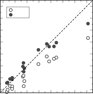
Even more importantly than the improvement in structure and energetics, the
PBE0 substantially improves the calculated band gaps [40]. This is shown in
Figure 7.1. The improvement is especially evident for materials such as Ge or InN
which have a vanishing or even negative band gap in semilocal approximations.
However, it is also evident that the improvement of the PBE0 over the PBE is not
systematic. In the PBE0, band gaps are overestimated for low band-gap materials and
underestimated for large band-gap ones. The best agreement is thus for intermediate
band-gap materials. It is also clear why the fraction a ¼ 0:25 is just a good
compromise rather than a universal parameter. In fact for both the PBE and the
PBE0 the dependence of the theoretical gap on the experimental one is approximately
described by a concave function. For PBE0 (a ¼ 0:25), the concave function crosses
the diagonal defined by E
th
g
¼ E
expt
g
at about 5 eV. Hence, the theoretical band gaps are
overestimated for some materials and underestimated for others. This behavior
applies to hybrid functionals with any other reasonable mixing coefficient a.
7.2.2.1 Integrable Divergence
In calculations based on plane-wave basis sets and periodic boundary conditions,
exact exchange poses one more challenge due to the long-range nature of the
Coulomb interaction. In Fourier space this interaction is proportional to 1=q
2
, and
08642101214
experimental band
g
ap (eV)
0
2
4
6
8
10
12
14
theoretical band gap (eV)
PBE
PBE0
SiO
2
Si
HfO
2
SiC
InN
ZnO
Ge
CdTe
MgO
Ar
C
SnO
2
TiO
2
NaCl
GaAs
Figure 7.1 (online color at: www.pss-b.com)
Calculated versus measured single-particle
band gaps for 15 different materials. PBE: open
disks, PBE0: filled disks. Results for GaAs, C,
MgO, NaCl, and Ar are taken from Ref. [40];
results for InN and ZnO are taken from Ref. [60];
the result for SnO
2
is taken from Ref. [33];
the result for TiO
2
(anatase form) is taken from
Ref. [61]; results for Si, SiC (4H polytype), HfO
2
,
CdTe, and SiO
2
are from our calculations.
7.2 Computational Toolbox
j
115
thus diverges at small q. The singularity is integrable, but its straightforward
calculation would require very dense k-point meshes. Gygi and Baldereschi [62]
proposed a method to treat this singularity. In the matrix element of the exchange
operator, they normalized the integrand by substracting an auxiliary function which
admits an analytical integration over the Brillouin zone. This method is suitable to
be adapted to much sparser k-point samplings, including those limited to the sole
C-point [46]. The effect of the singularity of the exchange potential can be cast into
a correction to the G ¼ 0 term of the potential [46, 63]. The Fourrier transform WðGÞ
of the exchange interaction is then given by
WðGÞ¼
1
V
4p
G
2
for G 6¼ 0;
x for G ¼ 0;
8
<
:
ð7:6Þ
where V is the volume of the supercell and the singularity correction x is expressed as
x ¼ lim
c !0
1
ffiffiffiffiffiffi
pc
p
4p
V
X
G
e
cG
2
G
2
"#
: ð7:7Þ
The total energy of a system of N
el
electrons is thus corrected by a term axN
el
=2,
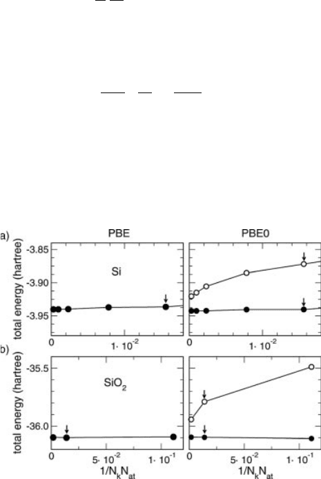
where a is the fraction of exact exchange used in the hybrid functional. In Figure 7.2,
we give the total energies of Si and SiO
2
as a function of the supercell size and/or the
density of the k-point mesh for both PBE and PBE0 functionals [46]. In the latter
case, the total energies are given with and without the singularity correction. When
Figure 7.2 Total energies of (a) Si and (b)
a-quartz SiO
2
per formula unit versus 1/N
k
N
at
,
where N
k
is the total number of k-points
and N
at
the total number of atoms in the
supercell. Results obtained in the PBE and
the PBE0 are reported in left and right panels,
respectively. For PBE0, closed and open
symbols indicate values obtained with the
singularity correction turned on and off,
respectively. Arrows show data points
which were also obtained with C-point
sampling.
116
j
7 Defect Levels Through Hybrid Density Functionals: Insights and Applications
the correction is included, the convergence properties of PBE0 calculations closely
resemble those of PBE calculations. Without the singularity correction the conver-
gence properties clearly deteriorate.
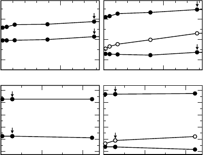
The singularity correction also affects the single-particle eigenvalues. Eigenvalues
of unoccupied states remain unchanged, while those of occupied ones shift by ax.
This is demonstrated in Figure 7.3 for the cases of Si and SiO
2
. When the singularity
correction is included, hybrid-functional calculations converge as fast as those based
on semilocal functionals. This equally holds for calculations with k-point samplings
restricted to the C-point. Singularity corrections apply equivalently to both deloca-
lized bulk-like states and localized defect or molecular states [46].
Furthermore, singularity corrections are particularly useful in the case of elon-
gated supercells, which may otherwise show an unphysical convergence behav-
ior [46]. Even in the case of screened hybrid functionals which do not show any formal
singularity, an analogous treatment of the q ¼ 0 limit may lead to a speed up of the
convergence with k-point sampling [46].
7.3
General Results from Hybrid Functional Calculations
As shown above, hybrid functionals containing a fixed fraction of exact exchange,
such as the PBE0 functional, do not bring theoretical band gaps in agreement with
0
1×10
-2
5
6
7
ε (eV)
0
5×10
-2
1×10
-1
1/N
k
N
at
0
2
4
6
8
10
ε (eV)
0
1×10
-2
0
5×10
-2
1×10
-1
1/N
k
N
at
a)
b)
PBE PBE0
SiO
2
Si
ε
c
ε
v
ε
c
ε
v
Figure 7.3 Eigenvalues corresponding to the
valence (e
v
) and conduction (e
c
) band edges of
(a) Si and (b) a-quartz SiO
2
versus 1/N
k
N
at
,
where N
k
is the total number of k-points and N
at
the total number of atoms in the supercell.
Results obtained in the PBE and the PBE0 are
reported in left and right panels, respectively.
For PBE0, closed and open symbols indicate
values obtained with the singularity correction
turned on and off, respectively. Arrows show
data points which were also obtained with
C-point sampling. The energies obtained with
the two functionals are aligned through the
average electrostatic potential (cf. Ref. [13]).
7.3 General Results from Hybrid Functional Calculations
j
117
experimental ones for all materials. Thus, while their straightforward application to
the determination of defect levels is expected to lead to an improvement with respect
to semilocal functionals, the comparison with experiment remains ambiguous.
Nevertheless, we can gain insight into how calculated and measured defect levels
should be compared by performing a comparative study between defect energy levels
calculated with semilocal and hybrid density functionals. Such a study is expected to
reveal how defect levels shift as the description of the band gap improves [13, 64, 65].
To this end, we find useful to refer charge transition levels calculated with different
functionals to a common reference potential w. We denote such charge transition
levels by
eðq=q
0
Þ(cf. Eq. 7.4). In our pseudopotential supercell approach, w is obtained
from the supercell average of the sum of the local pseudopotential and of the Hartree
potential. We argue in the following that this alignment is a convenient choice for
determining energy-level shifts induced by the hybrid functional with respect to
a reference semilocal calculation.
7.3.1
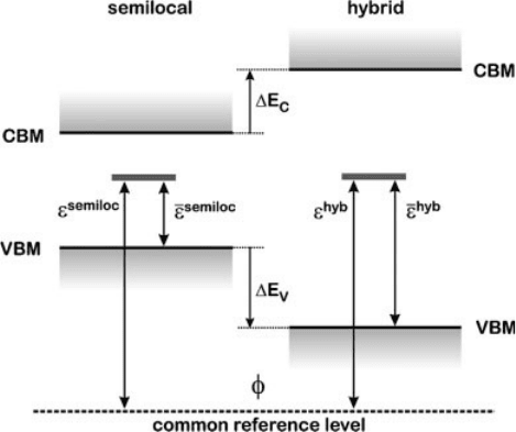
Alignment of Bulk Band Structures
In this section, we focus on the alignment of bulk band structures obtained with
semilocal and hybrid functionals. To simplify the reasoning, let us assume that
the same supercell parameters and the same pseudopotentials are used in the two
calculations [66]. In this case, the pseudopotential contribution to w is the same in the
two calculations, and the adopted alignment consists in aligning the average
electrostatic potential in the two theoretical schemes. This alignment allows one to
position band edges in the hybrid calculation with respect to those in the semilocal
one, i.e., to determine the shift of the VBM DE
V
and the conduction band minimum
(CBM) DE
C
on a common energy scale, as shown in Figure 7.4.
To analyze the significance of the adopted alignment scheme, it is convenient to
conceptually refer to the band offset at the interface between two materials, A and B.
The band offset is a well-defined physical property that can be measured. Following
the scheme introduced by Van de Walle and Martin [67], band offsets can be
determined by three calculations, namely an interface calculation from which one
extracts the line-up of the local average electrostatic potential across the interface and
two bulk calculations of materials A and B which allow one to locate the band edges
with respect to the respective average electrostatic potential in each material. This
procedure can separately be carried out for the semilocal and for the hybrid scheme.
Alternatively but equivalently, the band alignment in the hybrid scheme can also be
obtained from the alignment in the semilocal scheme by the consideration of three
sources of difference. By comparing the charge densities in the interface calculations
performed at the semilocal and hybrid levels, one can extract the difference in line-up
of the average electrostatic potential. Such a difference directly results from the
dipoles associated to the difference between the charge densities in the semilocal and
in the hybrid schemes. The two other sources of difference can be achieved by
separately comparing semilocal and hybrid calculations for bulk materials A and B.
The required differences correspond precisely to the shifts undergone by the band
118
j
7 Defect Levels Through Hybrid Density Functionals: Insights and Applications
edges when aligned with respect to the average electrostatic potential. This reasoning
thus illustrates that the band offsets in the hybrid scheme would be obtained by
combining information that can only be extracted from charge density variations as
derived from interface calculations with information that can be derived by aligning
the energy scales of periodic bulk calculations as proposed.
In the particular case in which material B is the vacuum, we are concerned with a
surface system. In this case, it is more natural to adopt the vacuum level at a large
distance from the interface as the common reference level for the semilocal and
hybrid calculations. From the reasoning in the previous paragraph, it appears clearly
that this alignment scheme is not equivalent to the one proposed in this work. Indeed,
the alignment to the vacuum level explicitly includes the consideration of a surface
and correspondingly charge density differences between the two theoretical schemes
might lead to different line-up terms, which would in turn determine a different
alignment. Hence, we stress once again that the alignment adopted here is concep-
tually particularly convenient because it highlights effects of the different theoretical
formulations as they result from bulk calculations, without the need for an explicit
treatment of interface or surface systems. However, the connection with measurable
properties such as work functions and band offsets cannot be made unless such an
explicit treatment is considered.
When the charge density is invariant in the two theoretical schemes under
comparison, the difference in line-up term vanishes and relative shifts in the
Figure 7.4 (online color at: www.pss-b.com)
Charge transition levels calculated within a
semilocal and a hybrid functional scheme,
aligned to a common reference level w. e is
the charge transition level referred to the
respective VBM (Eq. 7.2),
e is the charge
transition level referred to the level w (Eq. 7.4).
DE
V
and DE
C
are the shifts of the VBM and
of the CBM in the hybrid-functional
calculation with respect to the respective
edges in the semilocal calculation. Adapted
from Ref. [13].
7.3 General Results from Hybrid Functional Calculations
j
119
presence of an aligned electrostatic potential also acquire direct physical significance.
In practical calculations involving semilocal and hybrid calculations, this condition is
very close to being satisfied, as demonstrated for both interface [68] and surface
systems [69]. In such cases, the relative band-edge shifts determined through an
alignment of the average electrostatic potential give the dominant contribution to the
variations undergone by the band offsets [68]. In the case of invariant charge
densities, the alignment with respect to the average electrostatic potential is fully
equivalent to the alignment with respect to a an external vacuum level achieved
through the consideration of a surface.
7.3.2
Alignment of Defect Levels
Once the bulk band structures in the two theories are aligned as described in
Section 7.3.1, the alignment of charge transition levels is trivial. This is shown in
Figure 7.4. Hitherto, the common reference w was taken to be the average electro-
static potential, but it can for convenience be shifted to coincide with the VBM in the
hybrid calculation. In this case
e
hyb
ðq=q
0
Þ¼e
hyb
ðq=q
0
Þ, and
e
semiloc
ðq=q
0
Þ¼
e
semiloc
ðq=q
0
ÞþDE
V
, DE
V
being the shift of the valence band in the hybrid calculation
with respect to that in the semilocal one.
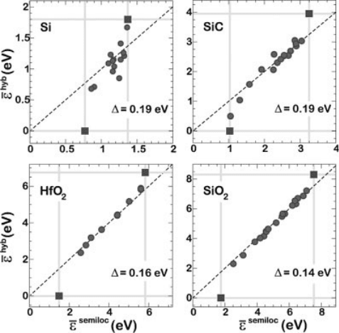
In Figure 7.5, we compare charge transition levels
eðq=q
0
Þ calculated with a
semilocal functional (PBE) with corresponding ones obtained with a hybrid func-
tional (PBE0) for a large set of deep defects in four different materials [13]. The chosen
materials show band gaps covering a wide range of values: Si (with an experimental
band gap of 1.17 eV), 4H–SiC (3.3 eV), monoclinic HfO
2
(5.75 eV), and a-quartz SiO
2
(8.9 eV).
Let us first focus on the defects in SiO
2
[64]. Due to the very different band gap of
SiO
2
in PBE (5.4 eV) and in PBE0 (7.9 eV), charge transition levels referred to the
respective valence band maxima differ significantly. At variance, when the charge
transition levels of these defects are referred to the average electrostatic potential,
they are very close in the two theoretical schemes. The mean deviation from the ideal
alignment is only 0.14 eV. This value is only indicative since it depends on the adopted
set of defects. Nevertheless, the alignment of charge transition levels is surprisingly
good over a large range of energies. The same alignment property approximately also
holds for other materials. For example, in HfO
2
the defect set includes oxygen
vacancies and interstitials and the correspondence is similarly very good, with mean
deviation of 0.16 eV. The departure from the ideal alignment [
e
hyb
ðq=q
0
Þ¼
e
semiloc
ðq=q
0
Þ] is only slightly larger in SiC and in Si, with a mean deviation of 0.19 eV
in both cases.
A detailed inspection reveals that defect levels in the upper part of the band gap
tend to shift upwards while those in the lower part tend to shift downwards as the
band gap is opened. It was found numerically that the deterioration from the ideal
alignment correlates with the increase of the average spread of defect wave func-
tions [13]. In this respect, SiO
2
is an optimal case, because the defect states in this
material are characterized by very localized wave functions.
120
j
7 Defect Levels Through Hybrid Density Functionals: Insights and Applications
These results can be understood by drawing an analogy between charge transition
levels of defect states and ionization potentials or electron affinities of atoms and
molecules [13]. The latter quantities can be expressed as total-energy differences and
are already well described in semilocal approximations [70, 71], as demonstrated by
extensive quantum chemistry calculations [72]. Typical mean deviations of about
0.2 eV are found between calculated and experimental results. Through the use of the
Slater–Janak transition-state theory [73, 74], the total energy difference appearing in
Eq. (7.4), i.e., E
D;q
tot
E
D;q
0
tot
, can be related to a matrix element of the defect state at half
occupation, which can then be rationalized to carry the same properties as atomic or
molecular states insofar its wave function is sufficiently localized [13, 64]. The ideal
alignment
e
hyb
ðq=q
0
Þ
e
semiloc
ðq=q
0
Þis therefore expected to hold best for atomically
localized defects and to deteriorate with the extension of the defect wave function.
The correspondence between energy levels in semilocal and hybrid functional
schemes does not hold for single-particle eigenvalues of extended bulk-like states, as
can be inferred from Figure 7.5 for various materials. We stress that this effect should
be explained by invoking the delocalized nature of these states rather than a different
behavior of eigenvalues and total-energy differences. In fact, the energy of the VBM
E
V
(and likewise for E
C
), appearing in the definition of the charge transition level in
Figure 7.5 (online color at: www.pss-b.com)
Comparison between charge transition levels
calculated with a semilocal (
e
semiloc
) and a
hybrid (
e
hyb
) functional for a variety of defects in
Si, SiC, HfO
2
, and SiO
2
. The energy levels
corresponding to the VBM and CBM are also
shown (squares). All energies are referred to
a common reference level w (see text), shifted to
coincide with the VBM in the hybrid scheme for
convenience. For each material, D is the r.m.s.
error with respect to the ideal alignment
(dashed). Adapted from Ref. [13].
7.3 General Results from Hybrid Functional Calculations
j
121
Eq. (7.2), can also be expressed through a total-energy difference: E
V
¼ E
bulk;0
tot
E
bulk; þ
tot
. However, for delocalized states, in sharp contrast to localized ones, this
total-energy difference is subject to large variations when calculated in semilocal and
hybrid functional schemes, reflecting the effect of the band-gap problem in the
same way as single-particle eigenvalues do. This is the main reason why defect charge
transition levels in different theoretical schemes differ so much when referred to
their respective valence band maxima.
The use of the unknown exact functional [75, 76] would in either case lead to a
correct description of the total energies of localized and extended states. The different
description of localized and extended states can be related to specific properties of the
approximate functional adopted [70, 71, 77, 78]. The success of approximate func-
tionals in describing total energies of localized systems is related to their fulfillment
of the sum rule for the exchange–correlation hole [70]. This stringent criterion is
fulfilled at integer electron numbers, yielding accurate total energy differences in
calculations for atomic and molecular systems [72]. However, such approximate
energy functionals fail in reproducing the linear behavior of the exact functional for
fractional electron numbers [75, 76]. As has recently been shown by Mori-S
anchez
et al. [78], this failure is at the origin of the incorrect description of single-particle
eigenvalues and total energies of delocalized systems. Thereby, these theoretical
results establish a clear relation between the band-gap problem of approximate
density functionals and the delocalized or localized nature of electronic states [78].
Over which length scales the transition takes place between localized and delocalized
states is at present still a matter of debate. For an interesting discussion on this issue,
we refer to Ref. [71].
The results of this section have provided useful indications concerning the way the
band-gap problem affects energy levels of deep defects. Defects localized on an
atomic scale appear to be already well described at the semilocal level when referred to
the average electrostatic potential. In particular, this implies that energy separations
between such defect levels are accurately described at the semilocal level and barely
affected by the band-gap problem. The calculations indicate that when the defect
state becomes more extended this ideal alignment tends to deteriorate. The short-
coming due to the band-gap problem only affects delocalized states such as the
valence and conduction band edges. While this of course hinders the correct location
of defect levels within the band gap, it nevertheless provides significant insight into
the way corrections should be made.
7.3.3
Effect of Alignment on Defect Formation Energies
The fact that charge transition levels of deep defects calculated at different levels of
theory tend to be aligned when referred to the average electrostatic potential has
important implications for the formation energies of charged defects.
In Figure 7.6, we give a diagram which schematically shows the formation energies
of a defect in the positive and the neutral charge state as a function of the electron
chemical potential, when calculated with a semilocal (dashed lines) or with a hybrid
122
j
7 Defect Levels Through Hybrid Density Functionals: Insights and Applications