Baca A.G., Ashby C.I.H. Fabrication of GaAs Devices
Подождите немного. Документ загружается.

Ohmic contacts
the contact), while the intercept gives twice the contact resistance
(R
c
= 0.03 -mm in this example). The contact resistance R
c
is
the most important value for planar devices such as FETs as it dir-
ectly relates to the parasitic resistances encountered in the device.
Furthermore, it is simple to measure and it requires no model to
extract. However, it is unsatisfactory from the standpoint of the
device metallurgy because it contains elements of semiconductor
resistance in addition to interfacial resistance as seen in the defini-
tion of FIGURE 6.2. One would prefer a more direct link between
the chemistry of the interface and its electrical properties. For this
reason, the contact resistivity r
c
of EQN (6.3) is more appropriate
and other models have been developed to extract r
c
from a planar
contact.
I
I
I
I
(a)
(b)
FIGURE 6.9 Plot of resistance
versus contact separation to extract
contact resistance.
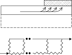
The geometry of a planar contact is shown in more detail
in FIGURE 6.9(a). In the planar contact model, it is assumed
that a semiconducting region is sandwiched between a semi-
insulating substrate and the contact metal. The resistance of the
semiconductor-contact combination can be modelled by a resistive
transmission line with uniform sheet resistance R
s
, as illustrated
in FIGURE 6.9(b) and as modelled by Berger [5]. Standard
microwave methods are used to determine the voltage and current
distributions along the transmission line:
V(x) = V
1
cosh(γx) − I
1
Z sinh(γx)
I(x ) = I
1
cosh(γx) − V
1
Z sinh(γx)
(6.9)
where Z is the characteristic impedance of the transmission line
and γ is the propagation constant. The equations for Z and γ are
given by [4]:
Z = R/G
1/2
= w
−1
(r
c
R
sh
)
1/2
(1 + jωCr
c
)
−1/2
γ = (RG)
1/2
= (R
sh
/r
c
)
1/2
(1 + jωCr
c
)
−1/2
(6.10)
The analysis can be restricted to the direct current case (ω = 0).
If the contact is assumed to be infinite in length, then Z = R
c
and
the equations simplify to
R
c
= w
−1
(r
c
R
sh
)
1/2
γ = 1/L
t
= (R
sh
/r
c
)
1/2
(6.11)
where L
t
is the transfer length. The definition of a transfer length
is motivated by the fact that in a contact of infinite length, most of
the current will flow from the semiconductor to the contact over
192
Ohmic contacts
a finite length near the edge of the contact. This length, the transfer
length, is proportional to the square root of the contact resistance
and inversely proportional to the square root of the sheet resistance.
The relationships contained in EQNS (6.11) are used in combin-
ation with the measured contact resistance of EQN (6.8) to derive
contact resistivity and transfer length for GaAs-based ohmic con-
tacts. However, it is important to realise that the sheet resistance
of EQNS (6.11) is the sheet resistance under the contact, which
is likely to be different from the measured sheet resistance of the
semiconductor between the contacts. The sheet resistance under
the contact is likely to be lower due to the fact that most alloyed
or sintered contacts introduce a heavily doped region directly under
the contact. In addition, spiking of the contact can further degrade
the assumption of a uniform conducting region under the contact.
In fact, there is no good way to measure the sheet resistance under
an ohmic contact. Despite this fact, many researchers prefer to use
EQNS (6.11) under the assumption that the sheet resistance under
the contact is the same as that of the semiconductor between the
contacts. Unfortunately, there is no good understanding of the error
introduced by this assumption. Because of the limitations in these
assumptions, it is prudent to be sceptical of any claims of con-
tact resistivity less than 10
−6
-cm
2
, as measured from a planar
contact (as is the case for the example in FIGURE 6.8, where r
c
is calculated as 4 × 10
−8
-cm
2
).
A method does exist in principle to measure the sheet resist-
ance under an ohmic contact and is described by Williams [4].
The method depends on the experimental analysis of the data in
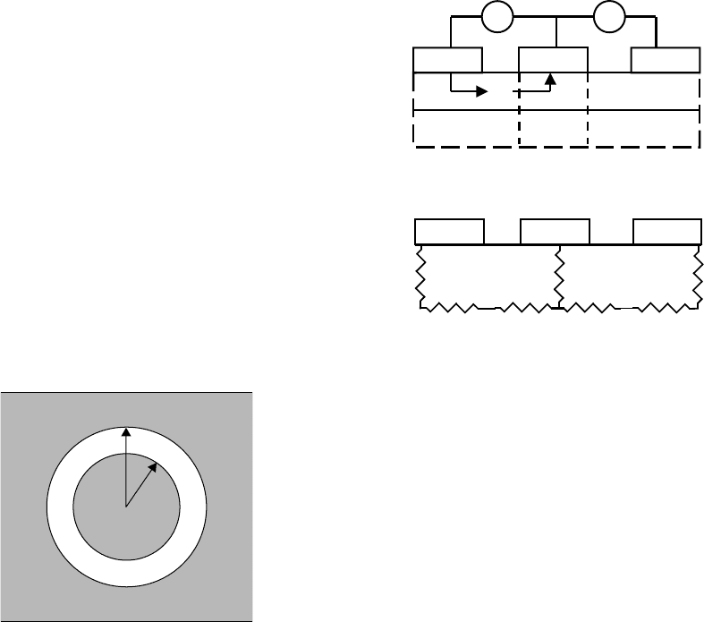
FIGURE 6.8 and on the measurement of the end resistance of the
contact geometry illustrated in FIGURE 6.10. A current I is forced
through the first two contacts. The voltage measured at the end of
the second contact (x = d) divided by the current at the beginning
of the second contact is the end resistance R
E
, which is given by:
R
C
/R
E
= cosh(d/L
t
) (6.12)
In principle, the measurement of R
E
is straightforward, but for
GaAs semiconducting regions with low resistivity, the length of
the contact should not be greatly larger than the transfer length L
t
for this method to work. In practice, L
t
is often less than 1 μm for
good GaAs contacts and the end resistance method is problematic.
Of the many ohmic contact test structures available, the linear
contact array is most commonly used with the planar contacts of
FETs and HBTs. However, one other useful structure is worth
discussing. The circular TLM [6], illustrated in FIGURE 6.11,
gives much of the same information as the linear contact array,
193
Ohmic contacts
I V
I
x =d
123
R
E
R
C
–R
E
R
C
–R
E
x =0
FIGURE 6.10 The end resistance method using a perfect current source and
high-impedance voltage monitor.
but does so without the need for an isolation step (or a pat-
terned implant). The circular TLM also takes up more space than
the linear contact array for a comparable contact pad dimension.
For this reason it may not be appropriate as an in-process dia-
gnostic, but rather is most useful for rapid turnaround in contact
optimisation experiments.
r
2
r
1
FIGURE 6.11 Illustration of the
circular TLM.
The geometry of a circular TLM makes the resistance calcula-
tion slightly more complicated, but still straightforward. If r
1
is
the inner radius and r
2
is the outer radius, and d the difference
between the two, then the resistance is given by
R = R
sh
/2π[L
t
(r
−1
2
+ (r
2
− d)
−1
+ ln[r
2
(r
2
− d)
−1
])] (6.13)
where other terms have been defined previously. EQN (6.13) is a
simplification of a more exact equation containing modified Bessel
functions which applies as long as the radii are greater than L
t
by
a factor of four or more.
Practical aspects of the measurement of ohmic contacts are key
to achieving consistent results. Measurements of adjacent con-
tacts in a linear contact array are generally made with a setup that
can be as simple as a probe station connected to a current source
and a voltmeter, although semiconductor parameter analysers are
much more flexible to set up and control. A width of 100 μm for
the contact array is typical. This width is large enough to easily
probe each pad with two probes. Spacings between contacts need
to be small enough that the resistance between contacts is not a
large fraction of the expected intercept (illustrated in FIGURE 6.8)
and are generally made small enough to comfortably print with
194
Ohmic contacts
medium-resolution optical lithography. Errors in the actual versus
intended spacing will directly limit the accuracy of the measure-
ment. For this reason, the spacings are not made so small that the
lithography is not reproducible. Commonly, the smallest gap is in
the range of 2–4 μm.
The resistance of the probes must be taken into account. The
intercept of the resistance data from a linear contact array is in
the range of several ohms for a 100 μm contact width for a state-
of-the art contact. A probe contacting the pad may have a resistance
that varies from 1–4 and introduces errors comparable to the
value of the resistance being measured. Elements of probe res-
istance include its material composition (tungsten tips penetrate
pads well but are more resistive) and changes in the pressure on
the pad each time it is placed in contact with the pad. Also, its
location on the pad will cause variability in the resistance if the
pad metal is somewhat resistive. Contact pads with an Au over-
coat, usually a separately deposited pad metal, do not generally
suffer from this latter problem. A separate step for the pad metal
avoids forming excessive amounts of AuGa at the surface of the
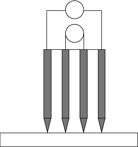
pad. A four-point probe measurement illustrated in FIGURE 6.12
will eliminate the probe resistance and lend greater accuracy to
the ohmic contact resistance measurement. Two of the probes are
used to force a known current through the adjacent contacts. The
remaining two probes are used to sense the voltage across the
contact pads. Voltage measurements are less sensitive to probe
resistance or other probe contact variability issues.
sample
I
V
FIGURE 6.12 Illustration of the
four-point probe method.
6.4 OHMIC CONTACTS TO n-TYPE GaAs
A wide variety of contacts to n-type GaAs have been investigated
over the years. Of these, the GeAuNi contact is now the most
widely used. Much of the reason may be historical, as the GeAuNi
contact was first reported in 1967 [1] and was found over the years
to be a great improvement over the earlier In-based ohmic con-
tacts. When GaAs manufacturing first took off with light emitting
diodes followed by MESFETs in the 1970s and early 1980s, the
GeAuNi contact was the best contact available. Manufacturing
always brings the need to establish reliability and repeatable pro-
cesses. GeAuNi ohmic metals satisfactorily passed these hurdles
and became difficult to dislodge in spite of the numerous perceived
drawbacks. Nevertheless, other ohmic contacts are now in use
in both research institutions and manufacturing facilities in some
niche applications. This section will review the use of GeAuNi
contacts and some newer approaches to addressing the limitations
of GeAuNi.
195
Ohmic contacts
6.4.1 GeAuNi ohmic contacts
The reaction of the GeAuNi contact was used as an example of the
metallurgical reactions described in Section 6.2.3. Proper attention
to those principles and to good fabrication procedures as described
in Section 6.3.1 can lead to reliable and repeatable contacts. Good
surface preparation is critical as is optimising the alloying tem-
perature and time for the particular metal layers chosen. No one
optimum recipe exists. Rather, within the framework of the reac-
tions involved, several are possible. The Ge and Au thicknesses
are almost always chosen so that the composition in a perfectly
mixed alloy is near the eutectic composition. The Ni thickness is
often chosen to be between 15 and 30% of the sum of the Ge and
Au thicknesses. The total thickness of the layers does not seem to
matter very much, as long as the contact resistance is optimised as a
function of the alloy temperature and time. Often the Au and Ge are
co-evaporated so that they can melt as the eutectic temperature of
the alloy (361
◦
C) is reached, but this can be impractical with elec-
tron beam evaporators and layer by layer depositions can be just
as effective. Electrical contact resistivities less than 10
−6
-cm
2
are routinely achieved.
A common ohmic contact recipe:
26 nm Ge, 54 nm Au, 15 nm Ni
annealed at 400–420
◦
C for 0.5–3 min.
Sheet resistance of 2 /square can be
expected.
Some variations of the basic recipe give equally good results.
For example, Ni has been recommended as a first layer to achieve
more consistency, uniformity and less spiking [7]. The authors
of this work undoubtedly explored this idea with great care and
thoroughness. However, they did not publish any work comparing
the Ni-first contact with no special surface preparation against the
standard contact with careful surface preparation, as outlined in
Section 6.3.1. When the Ni-first contact was evaluated by other
groups, it was found that the recipe works as advertised, as long
as the thickness of the initial Ni layer is kept at or below a certain
thickness of near 5 nm. For groups that have good manufactur-
ing control of such thin layers, the Ni-first contact may be a good
choice. For other groups, the standard recipe with extra atten-
tion to surface treatment is preferred. In general, one will find
that many variations of the basic recipe will give excellent results.
The key is to perform a careful optimisation of contact resistance
using the parameters and experimental conditions suited to a given
laboratory.
Ohmic contact with thick Au overcoat:
26 nm Ge, 54 nm Au, 15 nm Ni,
200 nm Au annealed at 380–400
◦
C for
20–40 s. Sheet resistance of
0.3 /square can be expected.
Other permutations of a GeAuNi contact recipe are common as
well. In addition to minor variations in either the total thickness
or the thickness of individual layers, an extra Au overcoat is often
used. GeAuNi with the thicknesses quoted in this section will
leave the metal with a resistance of about 2 /square, which is
too high for most devices. An extra Au layer must be added in a
subsequent step, usually an interconnect step. Alternatively, one
196
Ohmic contacts
may choose to add the extra Au as part of the ohmic contact process
in order to minimise the amount of processing needed. The use of
an extra Au overcoat is advantageous for the measurement of the
contact resistance. Without the extra Au, the contact resistance
measurement can be sensitive to the placement of the probes on
the pads and also to the pad pressure. With the extra Au, the
metal resistance is lowered by a factor of ten and the resistance
through the metal pad and the probe contact resistance becomes
negligible.
One concern with the addition of extra Au is the potential for
greater reactions with Ga along with excess tendency to spike
during the alloying process. The presence of the Ni layers acts
somewhat as a barrier to Au diffusion during the alloying process.
However, at high enough temperatures, the Ni is reacting with Ge
and no longer acts as a diffusion barrier. As a result, the Au must
be controlled by limiting the thermal budget of the reaction. As for
any contact recipe, the contact resistance and morphology must be
carefully optimised with regard to the anneal conditions. Generally
speaking, the alloying process uses slightly lower temperature and
times for contacts with a thick Au overlayer.
Thermal budget refers to the maximum
temperature (or temperature-time
product) that a process can handle. It is
used to define the bounds of a process
and to create an optimum process
sequence.
The GeAuNi contacts have shown adequate reliability for many
applications. Nevertheless, there have been some concerns for
other applications. The temperature stability of GeAuNi limits
the temperature of any post-processing steps and reduces the flex-
ibility for processing GaAs. Temperature stability also limits the
use of GaAs for high-temperature electronics. Other concerns for
GeAuNi contacts are its use in extremely thin layers such as the
base of a pnp heterojunction bipolar transistor (Chapter 9) because
of its propensity to spike and because reliability in extremely thin
layers is unproven. For some of these reasons, alternative contacts
have been developed.
6.4.2 Limited Au contacts for improved thermal stability
Much effort has been expended to attain ohmic contacts with
improved thermal stability. Almost all of these approaches elim-
inate or severely limit the amount of Au in the contact in order to
remove the temperature restriction of the Au-Ga reaction. Perhaps
the most comprehensive effort has been directed towards contacts
based on solid-phase regrowth. The PdGe ohmic contact wasrepor-
ted in 1985 and was the first of a number of contacts that fall under
the general solid-phase regrowth mechanism [8]. In this contact
the Pd plays a similar role to the Ni in the GeAuNi contact. At tem-
peratures near 100
◦
C, Pd reacts with the GaAs to form Pd
x
-GaAs
complexes. This reaction serves to disturb the GaAs lattice for
later Ge incorporation as an n-type dopant. Likewise, the Pd forms
197
Ohmic contacts
more stable compounds with the Ge, which acts as a driving force
for the removal of Pd from GaAs during a continuing temperat-
ure ramp and the regrowth of the GaAs with the incorporation
of a Ge dopant. The Pd-Ge alloy is stable up to temperatures near
600
◦
C, giving this contact more thermal stability than the GeAuNi
contact. The term solid-phase regrowth was used to describe this
reaction for two reasons. First, no eutectic melting takes place as
part of the alloying reaction, and therefore all reactions are solid-
phase. Second, the intermediate reaction of Pd with GaAs is only
temporary and the GaAs regrows as the Pd is removed from the
GaAs during the Pd-Ge reactions. Because of the absence of a Ga
consuming reaction, the PdGe contacts are suitable for shallow
contacts with excellent morphology and no spiking. Excellent res-
istivity comparable to GeAuNi contacts has been reported. Other
ohmic contacts based on solid-phase regrowth have been studied
as well, but the PdGe contact shows the best electrical properties of
these. In spite of the excellent thermal stability and good morpho-
logy, the PdGe contact is not as widely used as the GeAuNi contact,
but is an excellent choice for applications that require higher tem-
perature operation, extremely shallow contacts or greater edge
acuity. The main significant drawback of the PdGe contact is its
high resistivity, depending on the thickness. This drawback can be
remedied by the application of Au-containing interconnect.
Other Au-free contacts provide greater thermal stability. Simple
removal of the Au from GeAuNi also results in a contact stable
up to 600
◦
C. This contact is a close analogue of PdGe, but one
with slightly higher contact resistivity and a narrower optimum
composition. As such it is not very useful and would not even rate
a mention were it not for its improvement when small amounts of
Au are added. With as little as 3 nm of Au, the contact resistivity is
improved to within a factor of two of the GeAuNi contact without
adding so much Au that the morphology becomes poor. This con-
tact illustrates the principles of using the known metallurgical
mechanisms to engineer a contact with desired properties.
Other non-Au contacts worth noting are the GeAlNi and the
Cu
3
Ge contacts. The Al plays a similar role to the Au in GeAuNi.
However, the AlGe eutectic temperature (424
◦
C) is more than
60
◦
higher than that for AuGe, giving the contact higher thermal
stability. In addition to the higher eutectic temperature, stable
phases such as Al
3
Ni and NiGe compounds are formed within
the contact structure after sintering at 500
◦
C [9]. Another prom-
ising non-Au contact to n-type GaAs using Cu
3
Ge exhibits a planar
and abrupt interface and excellent contact resistivity of 6 × 10
−7
-cm
2
to moderately-doped GaAs (1 × 10
17
cm
−3
) [10]. Ohmic
contacts were observed with both excess Cu and excess Ge from
a stoichiometric Cu
3
Ge phase, suggesting that epitaxial Ge need
198
Ohmic contacts
not be a primary reason for the observed ohmic behaviour. In addi-
tion, Ga was observed by SIMS in the ε1-Cu
3
Ge phase suggesting
to the authors that Ga outdiffusion promotes Ge incorporation in
GaAs as an n-type dopant. These contacts can be considered if one
has concerns about other contacts in use. However, one might be
concerned about reliability of devices with active regions close to
the ohmic contacts since Cu diffusion is very rapid in GaAs.
6.4.3 Ohmic contacts to heavily doped surfaces
When the doping level increases above 10
19
cm
−3
, formation of
non-alloyed ohmic contacts through a tunnelling mechanism typ-
ically occurs and this will provide greater flexibility in the choice
of metal for the contact. Common n-type dopants have a dop-
ing concentration limitation of 2–4 × 10
18
cm
−3
in GaAs by ion
implantation and most commonly used epitaxy methods, but there
have been some novel methods to overcome this limitation. In one
such example Sn segregation to the surface of an n
+
GaAs layer
during MBE growth provided a sufficiently high surface concen-
tration to allow a non-alloyed contact based on TiPtAu, Al or TiW
metals [11]. Non-alloyed ohmic contacts using (NH
4
)
2
S surface
passivation followed by thermal desorption in vacuum have been
demonstrated, and it was suggested that the S incorporated below
the surface as an n-type dopant, raising the surface doping level
to 7 × 10
18
cm
−3
[12]. This topic is presented in more detail in
Section 3.3.4.
6.4.4 Refractory metals and contacts based on reducing the
surface bandgap
InAs with a bandgap of <0.4 eV and a surface Fermi level that is
pinned in the conduction band is a much better surface layer than
GaAs for an n-type ohmic contact. Accordingly, InAs or InGaAs
has often been used as an epitaxial surface contact layer for non-
alloyed ohmic contacts, when the device allowed such a structure.
The emitter surface of HBTs sometimes incorporates epitaxially
grown InGaAs layers for non-alloyed contacts to refractory metals
such as WSi [13].
Surface InGaAs is also a motivating factor in ohmic metal
structures containing In such as InW and NiInW. In-containing
contacts without the use of a refractory metal have in the past typ-
ically produced contacts with high contact resistivities of about
10
−5
-cm
2
or approximately one order of magnitude worse than
GeAuNi contacts. The poor results for the Au-, Ag- and Pt-In
contacts are due to uncontrollable, low-temperature, liquid-phase
reactions with GaAs. The use of a refractory metal with In has
199
Ohmic contacts
greatly improved this situation by producing contacts with res-
istivities that are nearly identical to GeNiAu contacts for InW [14]
and essentially identical by adding Si to the NiInW contact [15].
A number of other refractory In-containing contacts have been
reported as well. The refractory metal must be inert with the GaAs
at higher temperatures than conventional ohmic contacts, since the
InGaAs phases are formed and observed by TEM in the refractory
contacts only after alloying above 600
◦
C. Not surprisingly, the
thermal stability of these contacts at 400
◦
C is excellent. The role
of the refractory metal is to act as a barrier for a fairly thin In film
to maximise the coverage of InGaAs phases at the GaAs interface.
Films 3 nm thick were optimum for InW [14] with thinner films
not producing enough InGaAs and thicker films resulting in poor
thermal stability due to In-rich In(Ga,As) phases.
6.5 OHMIC CONTACTS TO p-TYPE GaAs
For Au-based ohmic contacts to p-GaAs, many of the same con-
siderations of GeAuNi n-type contacts are also relevant. The
metallurgical reactions outlined in Section 6.2.3 are mostly applic-
able to p-type contacts and mainly need to be modified by the
choice of elements needed for doping the GaAs. Though the prin-
ciples of Au-based and non-Au-based contacts to p-type GaAs are
similar to those for n-type GaAs in most respects, several distinct
differences exist. Metal contacts to p-type GaAs form lower bar-
rier heights, making thermionic-field emission a relatively easier
process for ohmic contact formation. Also, it is somewhat easier
to dope p-type GaAs above 10
19
cm
−3
for the formation of non-
alloyed ohmic contacts. Finally, the elements chosen to dope the
GaAs p-type and those chosen to promote an interface bandgap
lowering reaction are different for p-type contacts.
AuZn [16], AuBe [17] and TiPtAu [18] are some of the more
commonly utilised p-type contacts. These contacts lack the low-
temperature lattice disrupting constituents common to n-type
GaAs contacts. These contacts were developed two to three dec-
ades ago. Had the reaction mechanisms been better known at the
time, we might have seen AuZnNi or AuBeNi contacts developed.
Instead, the contacts were probably developed under the assump-
tion that a p-type dopant was needed to act in the place of the Ge for
an AuGe contact. Since no eutectic melting takes place with AuBe,
third element components were probably not thought necessary.
Small percentages of Zn or Be (e.g. 0.5–2% Be was found to
be optimum) were adequate for contacts in the low 10
−6
-cm
2
resistivity range. In these contacts, the Au provides the role of
a lattice disrupting element. No surface oxide reacting element
200
Ohmic contacts
is present, so the methods of surface preparation described in
Section 6.3.1 are critical. Also, the excess Be tends to diffuse to the
surface of the contact, where it oxidises and can form an insulating
barrier to a subsequent metallisation step or cause difficulties in
probing. Either the use of minimal amounts of Be in the contact, an
overcoat layer such as TiAu or a removal of the surface Be-oxide is
called for. The latter process can be accomplished with an HF dip.
AuBe contacts are usually thermally evaporated because electron
beam evaporation of the alloy quickly depletes the Be from the
surface of the alloy and causes problems for repeating the contact
composition in subsequent runs.
High p-type doping of GaAs is straightforward with epitaxy,
diffusion and ion implantation for a number of dopants including
Be, C, Mg and Zn. Non-alloyed ohmic contacts to these heavily
doped GaAs surfaces are then chosen based on other contact prop-
erties required by the given application. Non-alloyed contacts to
p-GaAs are the norm in most GaAs devices. TiPtAu contacts or
variants on these compositions are common for the base layer of
npn HBTs, where the doping is desired to be high to minimise
the base sheet resistance. Virtually any metal will make a non-
alloyed contact to the base layer of a highly doped npn HBT. Other
considerations determine the optimal composition. One popular
choice is the PtTiPtAu contact [19] with 15, 10, 15, 60 nm thick-
nesses of the layers. A composition of this type is chosen for
good adhesion, and the promotion of a uniform, shallow-reacted
contact (Section 6.4.2). Non-alloyed W and WSi contacts to p
+
regions based on shallow Zn and Mg implants are other types of
non-alloyed contacts that have been reported. These contacts have
approximately 1–2 × 10
−6
-cm
2
contact resistivity.
As is the case for n-type contacts to GaAs, a wide range of non-
Au metallisations exist as well. Many types of non-Au contacts
with improved morphology and/or temperature stability have been
reported for p-type GaAs. An example is NiSi(Mg) [20] which is
the p-type analogue of the n-type solid phase regrowth contact
using NiSi. Contact resistivity <10
−6
-cm
2
has been achieved.
Surface bandgap lowering contacts using NiInW(Mg) have been
reported [21] with contact resistance of 0.8 -mm. Contacts util-
ising both solid-phase regrowth and surface bandgap lowering
using PdSb(Mn) [22] with contact resistivity <10
−6
-cm
2
are
other examples.
6.6 CONCLUSION
Ohmic contacts to GaAs technology have been widely studied.
In part, this is due to the search for “greener pastures”. The
201