Baca A.G., Ashby C.I.H. Fabrication of GaAs Devices
Подождите немного. Документ загружается.

Schottky contacts
recess etching is possible. The process may be used for refractory-
gate self-aligned FETs, but such short gates become very difficult
to manage in a self-aligned process at gate lengths below about
0.4 μm. The encroachment of the self-aligned implants under the
gate creates a parallel channel under the gate that is difficult to con-
trol. Also, the gate resistance of WSi becomes quite high when the
gate is narrowed. A structure of this type will require some sort of
bilayer gate, as described in the next set of examples.
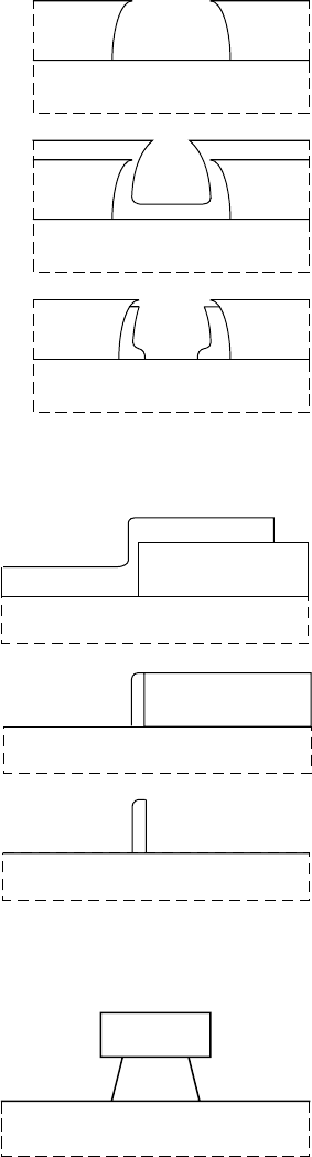
PR
dielectric
PR
PR
(a)
(b)
(c)
FIGURE 7.13 Illustration of
Y-gate process.
A bilayer gate process is commonly used in self-aligned pro-
cesses. The lower metal is chosen for its Schottky contact
properties, while the upper metal is chosen to provide a lower
gate resistance. A common choice is W/WSi, as illustrated in
FIGURE 7.15. Both metals can be defined by F-based reactive
ion etching. The W resistivity is about ten-fold lower than that of
WSi
0.45
. The WSi is sometimes undercut to provide a controlled
spacing from a drain implant relative to the gate edge. Although
liftoff is used to define an Au/Ti gate for recessed-gate structures,
the Ti may also be undercut by means of an F-based reactive ion
etch of the Ti, as for the W/WSi process. Other combinations of
metals are also possible. This procedure is sometimes used as a
method for tailoring the breakdown voltage.
WSi
(c)
(b)
(a)
SiN
x
SiN
x
FIGURE 7.14 Illustration of
sidewall gate process.
Another type of bilayer gate process is illustrated in
FIGURE 7.16. After a refractory gate (or angled evaporated gate)
is formed first as the lower gate, a dielectric is deposited over the
gate. This step is followed by a photoresist planarisation, which
is used in a subsequent etchback process. Often a CH
4
/O
2
gas
mixture is used with the gas ratio and other plasma conditions
adjusted for equirate etching of the photoresist and the dielectric.
The etchback proceeds until the lower gate is exposed. Then after
another photolithography step, the upper gate, usually Au-based,
is deposited by evaporation in a lift off process.
A variation of the last two bilayer gate processes is illustrated
in FIGURE 7.17. A bilayer structure using SiO
2
/WSi is formed
first by photolithography and RIE (FIGURE 7.17(a)). Then a
second photolithography step is used to form an opening about
the SiO
2
/WSi structure with the thickness of the resist chosen
appropriately for the next step (FIGURE 7.17(b)). The resist is
then reflowed to close the gap between the resist and the bilayer
structure (FIGURE 7.17(c)). The resist thickness is chosen so that
the dielectric protrudes above the reflowed resist. The dielectric is
then removed with an HF-based wet etch (FIGURE 7.17(d)), leav-
ing a re-entrant profile. In the last steps of the bilayer gate process,
an Au-based metal is deposited by evaporation for the final liftoff
step (FIGURES 7.17(e)–(f)).
As can be seen by these examples, many creative processes can
be used to achieve a given result.
FIGURE 7.15 Illustration of
bilayer gate process.
222
Schottky contacts
7.4 ELECTRICAL CHARACTERISTICS OF GaAs
SCHOTTKY CONTACTS
Interface states play a major role in the electrical properties of
Schottky contacts, as seen in Section 7.2.1. In turn, the treatment
of the GaAs surface prior to Schottky metal deposition will play
a part in determining these interface states. Even with clean sur-
faces, interface reactions of metal contacts with GaAs are the rule
rather than the exception. Although the interface reactions can vary
widely with the metal contact, they tend, in most cases, to produce
interface states and densities that fill to approximately midgap. For
these reasons, electrical properties of Schottky contacts with GaAs
vary little in comparison with certain electrical parameters (such
as metal work function, deemed important for contacts to other
semiconductors (e.g. Si)).
WSi
Au
SiN
FIGURE 7.16 Illustration of
bilayer gate process that utilises
dielectric etchback.
More than 40 elemental metals have been reported as Schottky
contacts to GaAs. Even more metal alloy combinations have been
studied. In one heroic study, 43 elemental metal Schottky con-
tacts were studied under the same experimental procedure for
consistency of the GaAs, the GaAs cleans and the metal deposition
procedure [10]. As has been discussed, consistency of the GaAs
surface history prior to metal deposition is a necessary requirement
for any hope of obtaining interface consistency. The GaAs was
grown by MOCVD and doped to 1×10
16
cm
−3
. All depositions
were carried out in an ultra-high vacuum system by electron-
beam deposition or resistive heating. The results are summarised
in TABLE 7.1. The Schottky barrier height, measured by the I-V
WSi
SiO
2
WSi
SiO
2
reflowed
PR
WSi
SiO
2
PR
(a)
(b)
(c)
PR
reflowed
PR
reflowed
PR
WSi
PR
WSi
(f)
(e)
(d)
WSi
TiAu
PR
FIGURE 7.17 Another bilayer gate process utilising a photoresist reflow
technique.
223

Schottky contacts
TABLE 7.1 Schottky contacts reported by
Myburg et al. [10].
Contact φ
B
(I-V) Contact φ
B
(I-V)
Mg 0.62 In 0.67
Al 0.77 Sn 0.71
Sc 0.71 Sb 0.97
Ti 0.83 Hf 0.81
V 0.80 Ta 0.78
Cr 0.80 W 0.79
Mn 0.82 Re 0.87
Fe 0.83 Ir 0.90
Co 0.83 Pt 0.99
Ni 0.83 Au 0.92
Cu 0.99 Pb 0.86
Zn 0.81 Bi 0.88
Ga 0.59 Pr 0.76
Y 0.71 Nd 0.76
Zr 0.77 Sm 0.75
Nb 0.77 Gd 0.75
Mo 0.87 Tb 0.75
Ru 0.86 Ho 0.74
Rh 0.89 Er 0.74
Pd 0.93 Tm 0.72
Ag 0.99 Yb 0.67
Cd 0.82
method, varied only from 0.6 to 1.0 eV for all metals studied. For
39 of the metals, the variation was only from 0.7 to 1.0 eV. For the
14 metals most commonly used as single layer contacts to GaAs
devices, φ
B
ranges from 0.77 to 0.99 eV. The ideality factor varied
from 1.01 to 1.03, a sign of high-quality contacts. Only a small cor-
relation was found to exist between the Schottky barrier height and
the metal work function, and only for a selected group of higher
melting point metals. Compilations of Schottky barrier properties
by other researchers generally arrive at similar conclusions.
The implications for FETs are as follows. Other things being
equal, the higher Schottky barrier height is usually preferred, as
it will generally produce lower leakage currents. In addition, it
allows higher forward bias and higher currents for enhancement-
mode transistors (those that are normally off at zero gate bias,
Section 8.2.1) that are widely used in digital circuits.
It should be noted that the barrier heights in MESFETs will
often be somewhat lower and ideality factors somewhathigher than
reported in TABLE 7.1 because the channel doping of MESFETs
is higher than 1 × 10
16
cm
−3
. In addition, surface conditions
are never as ideal for FET processing as for Schottky barrier
experiments and measurements in other laboratories can vary
224
Schottky contacts
somewhat from those reported in TABLE 7.1. HEMTs and HFETs
use higher bandgap materials (AlGaAs and InGaP) layers for the
Schottky interface. Nevertheless, the values in TABLE 7.1 offer
useful guidelines.
7.5 RELIABILITY OF GaAs SCHOTTKY CONTACTS
Issues that affect the reliability of GaAs-based Schottky contacts
can be categorised in three ways: interfacial reactions, degradation
of the interface and the underlying GaAs, and hydrogen poisoning
of GaAs FETs. Other FET reliability issues (Section 8.8) may also
involve Schottky contacts in more complex ways.
Interfacial reactions of the Schottky contact with GaAs are usu-
ally termed “gate sinking”, to denote the consumption of GaAs and
the associated movement of the Schottky interface. M-As or M-Ga
intermetallics can form a new interface with GaAs. The consump-
tion of GaAs results in electrical degradation of the FET, through
threshold voltage shifts and current reduction. Some common
interfacial reactions that occur in a short time period, generally
several hours or less, were described in Section 7.2.2. Many of
these same mechanisms will occur more slowly at lower temper-
atures according to the rate equation R = R
o
exp(E
a
/kT), but these
need to be verifiedforspecificcases. FET degradation(Section8.8)
is usually accelerated by either temperature or high electric fields,
but it is generally accepted that gate sinking is purely thermally
accelerated.
Most gate-sinking reliability studies have been carried out for
TiPtAu gates, and we will summarise some of these here. Stress
tests are usually thermally accelerated at temperatures above
225
◦
C and often approaching 400
◦
C. Gate sinking is positively
identified by a physical test such as TEM or X-ray diffraction
(Section 2.5) that reveals a degraded interface or new intermetallic
reaction phases. Once a mechanism is known for a given metal
system, electrical tests on Schottky diodes or FETs can be used
to detect failure. As previously noted, gate sinking will result in a
reduction in drain current for an FET, and it will result in a change
in either the Schottky barrier height (φ
b
), the ideality factor (n)
or the doping level for a Schottky diode. TiPtAu gates have been
observed to fail with an activation energy of 1.3–1.7 eV. Higher
stress-test temperatures naturally produce shorter average times
until device failure. The lower temperatures require longer stress
times but give greater confidence that another mechanism with
lower activation energy will not be the limiting one. It is pos-
sible that the range of activation energies represents differences
in gate metal processes. However, some studies indicate that the
225
Schottky contacts
higher activation energies represent gate sinking and the activa-
tion energy near 1.3 eV represents electrical degradation by carrier
reduction [8]. The likely explanation for the carrier reduction is
Ga outdiffusion during the initial interfacial degradation. Recall
from Section 7.2.2 that Ga diffusion into metals is a commonly
observed early step in M-GaAs interfacial reactions.
An extrapolated lifetime depends on the assumed operating
junction (gate) temperature for the FET, which will usually be
considerably higher than the ambient for a power FET and
closer to ambient for a low-noise FET. A junction temperature
of 125–150
◦
C is often assumed. Gate sinking mechanisms often
result in extrapolated median lifetimes greater than a million hours,
which means that they will not be a limiting factor in FET reli-
ability. Based on this mechanism, TiPtAu gates are considered
reliable by these criteria even though more stable alternatives exist
(Section 7.2.2).
One critical process condition is the thickness of the layers. Ti
and Pt thicknesses of 50–100 nm have been commonly used, but
Ti as thin as 30 nm is considered reliable [11] and will subject the
FET channel to lower stress.
In light of their excellent reliability against gate sinking, prop-
erly processed TiPtAu gates would not be considered a serious
reliability concern were it not for hydrogen poisoning. Due to
the use of hermetically sealed packages for high reliability space
applications, hydrogen can become trapped in the package. Kovar
material in the package is one source of the hydrogen. This
hydrogen causes degradation, as described below, but many other
sources of hydrogen exist, mainly from processing, and are dif-
ficult to control [12]. These include plasma processes such as
PECVD (Section 3.3.6) and hydrogen ion implantation.
Hydrogen can take part in several processes that change
Schottky barriers and FETs. It can passivate donors by bonding
with unpaired electrons that would otherwise be conduction band
carriers. A similar process works to passivate acceptors. Passiva-
tion of donors in FETs will reduce free carriers and cause threshold
voltage shifts and a reduction in other electrical parameters such
as the drain current. Pt or Pd are well-known catalysts for dissoci-
ating molecular hydrogen. When used as gate metal constituents
they can dissociate molecular hydrogen that builds up in hermetic
packages. The atomic hydrogen can then passivate donors in the
channel, causing positive threshold voltage shifts and a reduction
in channel current.
Another type of hydrogen poisoning has been observed in
FETs without involving the Pt in the gate. TiH was observed by
Auger spectroscopy (Section 2.5.2) in these FETs with hydrogen
poisoning and was believed to be the cause of the degradation. TiH
226
Schottky contacts
volume expansion and associated piezoelectric threshold voltage
shifts were believed to be the cause of the hydrogen poisoning
[13]. Since GaAs is a piezoelectric material, stress in the gate
causes a change in the electric field in the GaAs, causing shifts
in the threshold voltage of the FET. Hydrogen poisoning in TiAu
gates generally causes a lower degree of degradation than Pt- or
Pd-containing gates. In order to eliminate hydrogen poisoning,
it is necessary to place a hydrogen getter in the hermetic pack-
age or to eliminate the Ti and the Pt from the gate-metal stack.
At this time, it is not clear if hydrogen poisoning is a serious con-
cern in non-hermetic packages. Nevertheless, many manufacturers
are switching (or considering it) to WSi-based contacts, even for
low-temperature processes.
7.6 CONCLUSION
Schottky contacts are one of the most widely studied aspects
of GaAs technology. In part, this is due to the fact that no
single Schottky contact satisfies all of the requirements for an
ideal Schottky contact to GaAs. Another factor driving more
research has been the desire for higher Schottky barrier heights.
Yet another factor has been the poorly understood nature and
reproducibility of the metal/GaAs interface. In spite of the exist-
ence of contacts with greater interface stability, TiPtAu exhibits
more than sufficient reliability against gate sinking in GaAs-based
FETs. However, TiPtAu should be used with hydrogen getters
for hermetic packages or be replaced with non-Ti and non-Pt
materials. Many choices of refractory contacts can be used for
high-temperature self-aligned FETs. Some of the best are WSi
0.45
and WSiN because these remain amorphous to sufficiently high
temperatures. A wide variety of processing choices are available
to tailor the gate structure to the desired application using available
equipment.
REFERENCES
[1] S.M. Sze [Physics of Semiconductor Devices (John Wiley and Sons,
New York, 1981)]
[2] R. Williams [Modern GaAs Processing Methods (Artech House, Boston,
1990)]
[3] C.Y. Chang, F. Kai [GaAs High-Speed Devices: Physics, Technology, and
Circuit Applications (John Wiley and Sons, New York, 1994)]
[4] D.J. Coleman Jr., W.R. Wisseman, D.W. Shaw [Appl. Phys. Lett. (USA)
vol.24 (1974) p.355]
[5] C. Fontaine, T. Okumura, K.N. Tu [J. Appl. Phys. (USA) vol.54 (1983)
p.1404]
227
Schottky contacts
[6] K.B. Kim, M. Kniffin, R. Sinclair, C.R. Helms [J. Vac. Sci. Technol. A
(USA) vol.6 (1988) p.1473]
[7] Y. Kitaura, T. Hashimoto, T. Inoue, K. Ishida, N. Uchitomi [J. Vac. Sci.
Technol. B (USA) vol.12 (1994) p.2985]
[8] J.-L. Lee, J.K. Mun, B.-T. Lee [J. Appl. Phys. (USA) vol.82 (1997) p.5011]
[9] E. Nebauer, U. Merkel, J. Wurfl [Semicond. Sci. Technol. (UK) vol.12
(1997) p.1072]
[10] G. Myburg, F.D. Auret, W.E. Meyer, C.W. Louw, M.J. van Staden [Thin
Solid Films (Switzerland) vol.325 (1998) p.181]
[11] B.K. Seghal, B. Bhattacharyam, S. Vinayak, R. Gulati [Thin Solid Films
(Switzerland) vol.330 (1998) p.146]
[12] S.J. Pearton [Int. J. Mod. Phys. B (Singapore) vol.30 (1994) p.1247]
[13] R.R.Blanchard, A. Cornet, J.A. del Alamo [IEEE Electron Device Lett.
(USA) vol.21 (2000) p.424]
228
Chapter 8
Field effect transistors
Chapter scope p.229
Field effect transistor basics p.229
Field effect transistor tutorial p.230
Field effect transistor performance
and reliability issues p.236
Field effect transistor structures and
materials p.240
Overview of field effect transistor
fabrication p.244
Doping FETs p.247
Isolation of FETs p.251
Source and drain ohmic
contacts p.253
Gate metal contacts p.254
Passivation p.254
Degradation of FETs p.256
Definition and characterisation of
hot electrons p.257
Hot electron degradation p.260
Other types of degradation p.264
Conclusion p.265
References p.265
8.1 CHAPTER SCOPE
This chapter will cover most of the basic GaAs-related processing
steps for GaAs field effect transistors, including most of the front-
end steps. Active steps are those that relate to the fabrication of the
GaAs field effect transistor and do not include the interconnections
or the integration of passive elements. FET fabrication and opera-
tion require an understanding of the GaAs semiconductor surface
and its interface to metal junctions for etching, doping, contact
formation and some particular aspects of performance optimisa-
tion. This chapter will draw heavily on material presented in the
preceding chapters.
The basics of field effect transistors and their different types
are given in Section 8.2 [1–3]. That section starts with a tutorial
and continues to relate FET operation to the processing methods,
device geometries and materials. It also highlights the main reli-
ability issues and relates them to FET structures, processing and
materials. Sections 8.3, 8.4 and 8.5 present the details of the main
active processing methods: ion implantation, ohmic and Schottky
metal formation, recessed gate etching and passivation.
8.2 FIELD EFFECT TRANSISTOR BASICS
The field effect transistor was proposed long before it was demon-
strated in 1952. In the 1920s, semiconductors were poorly under-
stood because of poorly developed materials technology. Two of
the greatest materials problems of that time were a lack of pur-
ity and a lack of understanding of the semiconductor surface and
its oxides. Both of these areas saw great progress in the 1950s
with the development of zone refining methods of purification,
among other important developments. These developments were
followed by great progress in the development and understanding
of transistors, which ushered in the modern age of microelectronics
that has so radically changed our society in the latter half of the
twentieth century.
229
Field effect transistors
8.2.1 Field effect transistor tutorial
Our discussion of FETs begins with a simplified tutorial on
the operation and characterisation of field effect transistors.
Some knowledge of semiconductor physics is necessary, but
the transistor action is described without any prior knowledge
assumed. A more complete treatment of FET operation is given in
references [1–3].
The field effect transistor can be thought of as a voltage con-
trolled resistor. The transistor consists of three contact electrodes
and a semiconductor channel. The FET is known as a majority
carrier device, which means that transport is carried out by the
type of carriers, electrons or holes, which comprise the majority
of the carriers in the semiconductor. Either electrons or holes
can traverse the semiconductor channel, although electrons do so
with greater speeds. The three contacts are represented by the
nomenclature of source, gate and drain, which are schematically
illustrated in FIGURE 8.1. An electric potential is applied between
the source and the drain, which provides an impetus for carrier
transport, or current, to the drain along the semiconducting chan-
nel of the device. The source and drain contacts are ohmic contacts
and provide low-resistance paths across the metal/semiconductor
interface. Carriers for transport in the channel are provided by the
electrical dopants that are located in the channel region and are
generally absent outside the channel. The gate potential can mod-
ulate the carriers in the channel and, therefore, the magnitude of
the current from negligible levels to the maximum level. In this
way, the input voltage to the gate can cause the transistor to oper-
ate as a switch in digital circuits, or a signal amplifier in analogue
circuits. Ideally, no current flows into the gate, because this results
in a parasitic current which does not promote switching or signal
amplification.
source gate drain
channel
substrate
FIGURE 8.1 Schematic
cross-section of a field effect
transistor.
There are two main types of gate, the metal-oxide-
semiconductor (MOS) gate, which forms the basis of the dominant
CMOS Si technology, and the metal-semiconductor, or Schottky
gate, which is used for GaAs technology. Transistor action in GaAs
will be described in terms of the effect of a voltage applied to a
Schottky contact. The detailed physical description of a MOS gate
or other types of heterostructures with Schottky gates is somewhat
different, but the end effect of depleting or adding carriers with
the applied gate voltage is similar.
The basics of the Schottky contact are addressed in Chapter 7.
The key concept for understanding transistor operation is that the
potential of the Schottky contact (built-in potential plus applied
voltage) creates a depletion region, so named because free carriers
are depleted from this region and do not participate in the transport.
230
Field effect transistors
The depletion region can be made shallower by a positive forward
bias for an n-type FET up to the value where the Schottky barrier
is forward biased to turn on its diode. The depletion region can
be increased in depth by negatively biasing an n-type FET. When
the applied bias is sufficient to extend the depletion region com-
pletely across the doped channel region of the FET, the device
is “pinched off” and current flow from the source to the drain is
effectively stopped by being reduced to levels many orders of mag-
nitude below the on-state currents. This voltage is known as the
threshold voltage of the FET. Its value is an important parameter in
the design of devices for specific applications and is given by the
following expression for a MESFET with a uniform doping profile:
V
th
= (−qN
D
a
2
/2ε) + V
bi
(8.1)
where q is the electron charge, N
D
is the donor density in the
channel, a is the thickness of the doped channel, ε is the dielec-
tric constant of the semiconductor and V
bi
is the built-in voltage.
EQN (8.1) is derived from the expression for the depletion region of
a Schottky contact (Chapter 7). HFETs, HEMTs and MESFETs
with non-uniform channels will have other expressions for the
threshold voltage, which need not concern us here.
The transistor operation of an FET can be better understood
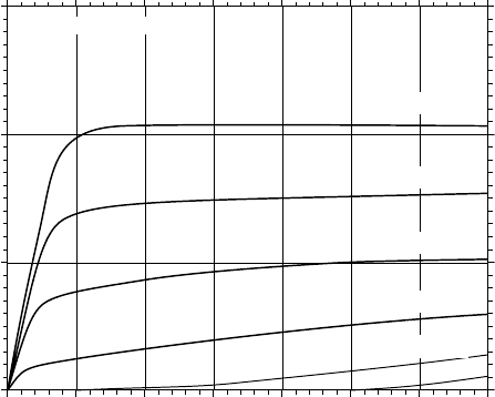
by examining some of the basic DC measurements. The most
common DC measurements are the drain I-V characteristics, illus-
trated in FIGURE 8.2. The drain current is plotted against the
drain voltage for a family of gate voltages which start with the
01234567
0
5
10
15
drain current (mA)
drain source bias (V)
0.4 × 40 μm
gate bias: 0.0 to 1.25 V
V
G
= 1.25 V
1.0 V
1.75 V
–0.5 V
–0.25 V
FIGURE 8.2 Drain I-V characteristics of an FET.
231