Cao Z. (Ed.) Thin Film Growth: Physics, materials science and applications
Подождите немного. Документ загружается.

398 Thin film growth
© Woodhead Publishing Limited, 2011
As can be seen in Fig. 16.8(a) and (b), the re-emission process which is
the dominant process in normal angle growth promotes an exponential degree
distribution; while shadowing which is the governing effect during oblique
angle deposition leads to a power-law distribution. On the other hand, CVD
shows an exponential degree distribution at initial times of growth, while it
becomes closer to power-law type for higher sticking coefcients, s > 0.5.
This is believed to be competing forces of re-emission and shadowing effects,
where the re-emission is more dominant for smaller sticking coefcients
and at initial times of the growth when the lm is smoother, leading to an
exponential degree distribution. However, the shadowing effect originating
from the obliquely incident particles within the angular distribution of CVD
ux can lead to a power-law behavior at higher sticking coefcients especially
when the lm gets rougher at later stages of growth. A power-law degree
distribution corresponds to a more correlated network that is consistent with
the long-range, column-to-column trafc observed in surface-degree plots
of high sticking coefcient CVD above (Fig. 16.6(b)). It is also realized
that especially for high sticking coefcients, there exist high degree nodes
represented with data points at the tails of the degree distributions. These
relatively small percentage but highly connected nodes are mainly located at
the column edges as seen in the surface degree plot of Fig. 16.6(b) and are
likely to be the ‘hubs’ of the network. Therefore, briey, degree distribution
during cVD growth can be similar to the universal line of normal incidence
growth for smaller sticking coefcients (s < 0.5) showing an exponential
behavior with a short range network trafc; or it can converge to the universal
power-law degree distribution of oblique angle deposition for higher sticking
coefcients (s > 0.5) leading to a highly correlated network driven mostly
at column edges.
In addition, it is revealed from average distance versus degree plots of
Fig. 16.8(c) and (d) that nodes with high degree are mainly linked with long-
distance surface points. Independent of the deposition method, the average
distance changes with degree k according to a power-law behavior, where
the value of the exponent increases as the ux becomes more oblique (i.e.,
A0 Æ A85 Æ CVD in Fig. 16.8(c) and (d)), sticking coefcient increases,
and the lm gets thicker (i.e., Fig. 16.8(c) Æ (d)). In other words, when
the shadowing effect becomes more dominant and lm morphology gets
more columnar, high degree nodes can exchange atoms with longer distance
surface points. This also implies that high degree nodes placed on column
edges (Fig. 16.6(b)) of high sticking coefcient growth are more likely to
transfer particles with other more distant column edges as well. This process
is further supported by the distance distribution plots of Fig. 16.8(e) and
(f) where as the sticking coefcient is increased (i.e. less re-emission) and
more obliquely deposited particles are introduced (more shadowing effect),
a higher percentage of particles start to travel longer distances. On the other
ThinFilm-Zexian-16.indd 398 7/1/11 9:46:41 AM
399Network behavior in thin films & nanostructure growth dynamics
© Woodhead Publishing Limited, 2011
hand, for smaller sticking coefcients and normal angle deposition, where
the re-emission effect is more dominant, average distances particles travel
from high degree nodes become signicantly less compared to high sticking
coefcient and oblique angle depositions. This suggests networking during
re-emission dominated growth occurs mainly among smaller size hills and
valleys, consistent with the surface-degree plot of Fig. 16.6(a).
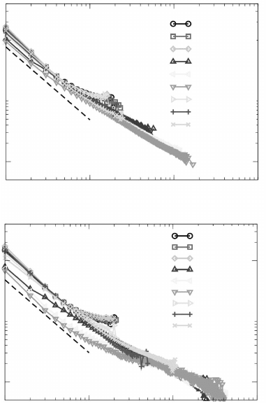
A more interesting universal behavior is observed in a ‘weighted and
scaled average distance’ versus degree plots of Fig. 16.9(a) and (b). Here
we re-scale average distance for nodes with degree k, <l
k
>, rst with degree
k, then with the average distance value of all nodes <l> (average distance
of all links), and plot <l
k
>/(k<l>) versus k. After re-scaling, independent of
the deposition technique used, sticking coefcients, and the growth time,
all curves fall on a similar line obeying a power-law behavior with <l
k
>/
(k<l>) ~ k
–1.2
. The origin of the –1.2 value of the exponent is not clear and
is under investigation.
Another universal behavior is observed in distance distribution plots.
Independent of sticking coefcients, normal incidence growth shows a
power-law behavior with P(l) ~ l
–3
. A similar power-law behavior with an
exponent of –2.75 has been observed in the distance distribution plots during
a normal incidence growth simulation with re-emission (p. 83 of Ref. [14]).
The authors of that work did not use a snapshot state approach, surface
morphology changed continuously, and therefore they measured a kind of
average distance distribution of the whole growth simulation. However, their
exponent value is still close to our results and agrees with our ndings that
dynamic network behavior during normal incidence deposition does not
change signicantly due to the relatively smooth morphology throughout
the growth. On the other hand, the behavior in distance distribution plots is
exponential for oblique angle deposition (conrmed in the semi-log plots,
not shown here). CVD has a power-law behavior similar to that of normal
incidence growth with P(l) ~ l
–3
at smaller coefcients and at initial times
of growth, and becomes exponential similar to oblique angle deposition at
higher sticking coefcients apparent especially in later stages of growth.
16.5 Conclusions
In conclusion, we presented a new network modeling approach for various
thin lm growth techniques that incorporates re-emitted particles due to the
non-unity sticking coefcients. We dene a network link when a particle is
re-emitted from one surface site to another. Monte Carlo simulations are used
to grow lms and dynamically track the trajectories of re-emitted particles.
We performed simulations for normal incidence, oblique angle, and CVD
techniques. Each deposition method leads to a different dynamic evolution
of surface morphology due to different sticking coefcients involved and
ThinFilm-Zexian-16.indd 399 7/1/11 9:46:41 AM
400 Thin film growth
© Woodhead Publishing Limited, 2011
different strength of shadowing effect originating from the obliquely incident
particles. Traditional dynamic scaling analysis on surface morphology cannot
point to any universal behavior. On the other hand, our detailed network
analysis reveals that there exist universal behaviors in degree distributions,
weighted average degree versus degree, and distance distributions independent
of the sticking coefcient used and sometimes even independent of the
growth technique. We also observe that network trafc during high sticking
coefcient CVD and oblique angle deposition occurs mainly among edges
of the columnar structures formed, while it is more uniform and short-range
among hills and valleys of small sticking coefcient CVD and normal angle
depositions that produce smoother surfaces.
A0, s = 0.1
A0, s = 0.5
A0, s = 0.9
A85, s = 0.1
A85, s = 0.5
A85, s = 0.9
CVD, s = 0.1
CVD, s = 0.5
CVD, s = 0.9
A0, s = 0.1
A0, s = 0.5
A0, s = 0.9
A85, s = 0.1
A85, s = 0.5
A85, s = 0.9
CVD, s = 0.1
CVD, s = 0.5
CVD, s = 0.9
10
0
10
0
10
–2
10
–2
<l
k
>/(k <l >)<l
k
>/(k <l >)
10
0
10
1
10
2
10
3
k
(a)
10
0
10
1
10
2
10
3
k
(b)
k
–1.2
k
–1.2
16.9 Weighted average distance <l
k
>/(k<l>) versus degree k for
network models of a Monte Carlo simulated normal incidence
evaporation (A0), oblique angle deposition (A85), and CVD thin
film growth for various sticking coefficients s and for two different
deposition times t (a: t = 1.25 ¥ 10
7
particles, and b: t = 23.75 ¥ 10
7
particles).
ThinFilm-Zexian-16.indd 400 7/1/11 9:46:41 AM
401Network behavior in thin films & nanostructure growth dynamics
© Woodhead Publishing Limited, 2011
16.6 References
[1] Smith D l (1995), Thin-Film Deposition: Principles and Practice, New York,
McGraw-Hill.
[2] Meakin P (1998), Fractals, Scaling, and Growth far from Equilibrium, cambridge,
cambridge university Press.
[3] barabasi A l and Stanley H e (1995), Fractal Concepts in Surface Growth,
cambridge, cambridge university Press.
[4] Young N O and Kowal J (1959), ‘Optically active uorite lms’, Nature, 183,
104–105.
[5] Motohiro T and Taga Y (1989), ‘The lm retardation plate by oblique deposition’,
Appl. Opt., 28, 2466–2482.
[6] Azzam R M (1992), ‘Chiral thin solid lms: method of deposition and applications’,
Appl. Phys. Lett., 61, 3118–3120.
[7] Robbie K, Brett M J and Lakhtakia A (1996), ‘Chiral sculptured thin lms’, Nature,
384, 616.
[8] robbie K, beydaghyan G, brown T, Dean c, Adams J and buzea c (2004),
‘Ultrahigh vacuum glancing angle deposition system for thin lms with controlled
three-dimensional nanoscale structure’, Rev. Sci. Instrum. 75, 1089–1097.
[9] Karabacak T and lu T M (2005), ‘Shadowing growth and physical self-assembly of
3D columnar structures’, in Rieth M and Schommers W, Handbook of Theoretical
and Computational Nanotechnology, Stevenson Ranch, CA, American Scientic
Publishers, 729.
[10] Karabacak T, Wang G C and Lu T M (2004), ‘Physical self-assembly and the
nucleation of three-dimensional nanostructures by oblique angle deposition’, J.
Vac. Sci. Technol. A, 22, 1778–1784.
[11] lakhtakia A and Messier r (2005), Sculptured Thin Films: Nanoengineered
Morphology and Optics, Bellingham, WA, SPIE Press.
[12] Family F and Vicsek T (1985), ‘Scaling of the active zone in the eden process
on percolation networks and the ballistic deposition model’, J. Phys. A, 18,
l75–l81.
[13] Family F (1986), ‘Scaling of rough surfaces: effects of surface diffusion’, J. Phys.
A, 19, L441–L446.
[14] Pelliccione M and lu T M (2007), Evolution of Thin Film Morphology: Modeling
and Simulations, New York, Springer.
[15] lu T M, Zhao Y P, Drotar J T, Karabacak T and Wang G c (2003), ‘Novel
mechanisms on the growth morphology of lms’, Mat. Res. Soc. Symp. Proc.,
749, 3.
[16] Pelliccione M, Karabacak T, and Lu T M (2006), ‘Breakdown of dynamic scaling
in surface growth under shadowing’, Phys. Rev. Lett., 96, 146105.
[17] Pelliccione M, Karabacak T, Gaire C, Wang G C and Lu T M (2006), ‘Mound
formation in surface growth under shadowing’, Phys. Rev. B, 74, 125420.
[18] Zhao Y P, Wang G c and lu T M (2001), Characterization of Amorphous and
Crystalline Rough Surfaces: Principles and Applications, San Diego, cA, Academic
Press.
[19] Family F and Viscek T (1991), Dynamics of Fractal Surfaces, Singapore, World
Scientic.
[20] Karunasiri R P U, Bruinsma R, and Rudnick J (1989), ‘Thin-lm growth and the
shadow instability’, Phys. Rev. Lett., 62, 788–791.
ThinFilm-Zexian-16.indd 401 7/1/11 9:46:41 AM
402 Thin film growth
© Woodhead Publishing Limited, 2011
[21] Karabacak T, Zhao Y P, Wang G C and Lu T M (2001), ‘Growth-front roughening
in amorphous silicon lms by sputtering’, Phys. Rev. B, 64, 085323.
[22] Karabacak T, Zhao Y P, Wang G c and lu T M (2002), ‘Growth front roughening
in silicon nitride lms by plasma-enhanced chemical vapor deposition’, Phys. Rev.
B, 66, 075329.
[23] Xu X and Goodman D W (1992), ‘Metal deposition onto oxides: an unusual low initial
sticking probability for copper on SiO
2
’, Appl. Phys. Lett., 61, 1799–1801.
[24] van Veldhuizen E M and de Hoog F J (1984), ‘Analysis of a Cu-Ne hollow cathode
glow discharge at intermediate currents’, J. Phys. D: Appl. Phys., 17, 953–968.
[25] Bogaerts A, Naylor J, Hatcher M, Jones W J and Mason R (1998), ‘Inuence
of sticking coefcients on the behavior of sputtered atoms in an argon glow
discharge: modeling and comparison with experiment’, J. Vac. Sci. Technol. A,
16, 2400–2410.
[26] Obara K, Fu Z, Arima M, Yamada T, Fujikawa T, Imamura N and Terada N
(2002), ‘collision processes between sputtered particles on high speed rotating
substrate and atomic mass dependence of sticking coefcient’, J. Crystal Growth,
237–239, 2041–2045.
[27] Migita S, Sakai K, Ota H, Mori Z and Aoki R (1996), ‘The inuence of Bi-sticking
coefcient in the growth of Bi(2212) thin lm by ion beam sputtering’, Thin Solid
Films, 281–282, 510–512.
[28] bogaerts A, Wagner e, Smith b W, Winefordner J D, Pollmann D, Harrison W
W and Gijbels R (1997), ‘Three-dimensional density proles of sputtered atoms
and ions in a direct current glow discharge: experimental study and comparison
with calculations’, Spectrochimica Acta Part B, 52, 205–218.
[29] Toprac A J, Jones b P, Schlueter J and cale T S (1995), ‘Modeling of collimated
titanium nitride physical vapor deposition using a combined specular-diffuse
formulation’, Mat. Res. Soc. Symp. Proc., 355, 575.
[30] Yamazaki O, Iyanagi K, Takagi S and Nanbu K (2002), ‘Modeling of Cu transport in
sputtering using a Monte Carlo simulation’, Jpn. J. Appl. Phys., 41, 1230–1234.
[31] liu D, Dew S K, brett M J, Smy T and Tsai W (1994), ‘compositional variations
in Ti-W lms sputtered over topographical features’, J. Appl. Phys., 75, 8114–
8120.
[32] buss r J, Ho P, breiland W G and coltrin M e (1988), in rubloff G W, Deposition
and Growth: Limits for Microelectronics, AIP Conf. Proc. 167, 34.
[33] buss r J, Ho P, breiland W G and coltrin M e (1988), ‘reactive sticking
coefcients for silane and disilane on polycrystalline silicon’, J. Appl. Phys., 63,
2808–2819.
[34] Tsai c c, Shaw J G, Wacker b and Knights J c (1987), ‘Film growth mechanisms
of amorphous silicon in diode and triode glow discharge systems’, Mat. Res. Soc.
Symp. Proc., 95, 219.
[35] Perrin J and broekhuizen T (1987), ‘Modeling of Hg(
3
P
1
) photosensitization of
SiH
4
and surface reactions of the SiH
3
radical’, Mat. Res. Soc. Symp. Proc., 75,
201–208.
[36] Perrin J and Broekhuizen T (1987), ‘Surface reaction and recombination of the SiH
3
radical on hydrogenated amorphous silicon’, Appl. Phys. Lett., 50, 433–435.
[37] Robertson R and Gallagher A (1986), ‘Mono- and disilicon radicals in silane and
silane-argon dc discharges’, J. Appl. Phys., 59, 3402–3411.
[38] Robertson J (2000), ‘Growth mechanism of hydrogenated amorphous silicon’, J.
Non-Cryst. Solids, 266–269, 79–83.
ThinFilm-Zexian-16.indd 402 7/1/11 9:46:41 AM
403Network behavior in thin films & nanostructure growth dynamics
© Woodhead Publishing Limited, 2011
[39] Drotar J T, Zhao Y P, lu T M and Wang G c (2000), ‘Mechanisms for plasma
and reactive ion etch-front roughening’, Phys. Rev. B, 61, 3012–3021.
[40] Karabacak T, Singh J P, Zhao Y P, Wang G c and lu T M (2003), ‘Scaling during
shadowing growth of isolated nanocolumns’, Phys. Rev. B, 68, 125408.
[41] Karabacak T, Wang G C and Lu T M (2003), ‘Quasi-periodic nanostructures grown
by oblique angle deposition’, J. Appl. Phys., 94, 7723–7728.
[42] Smy T, Vick D, brett M J, Dew S K, Wu A T, Sit J c, and Harris K D (2005),
‘Three-dimensional simulation of lm microstructure produced by glancing angle
deposition’, J. Vac. Sci. Technol. A, 18, 2507–2512.
[43] Boccaletti S, Latora V, Moreno Y, Chavez M and Hwang D U (2006), ‘Complex
networks: structure and dynamics’, Physics Reports, 424, 175–308.
[44] Watts D J and Strogatz S H (1998), ‘Collective dynamics of small-world networks’,
Nature, 393, 440–442.
[45] Barabasi A L and Albert R (1999), ‘Emergence of scaling in random networks’,
Science, 286, 509–512.
ThinFilm-Zexian-16.indd 403 7/1/11 9:46:41 AM

© Woodhead Publishing Limited, 2011
404
Index
adatoms, 11–15, 391
schematic illustration, 11
Ag lm, 26–7
all-order re-emission, 391
AlN, 297–300
angle-resolved photoemission
spectroscopy, 25–8
Ag on Fe(100) normal emission
photoemission spectra, 27
silver energy band structure, 26
anisotropic diffusion, 64
anisotropy, 55
anti-Bragg oscillations, 102–6
antiferroelectric thin lms, 370–1
Apollonius packing, 156
ARPES see angle-resolved photoemission
spectroscopy
atomic force microscope, 212
atomic force microscopy, 90, 233
atomic layer deposition, 70
atomic steps
morphological instability, 15–16
evolution of atomic step instability,
16
motion on growing and evaporating Si
(111) surface, 11–15
adatoms schematic illustration, 11
atomic steps temperature
dependence, 13
circular terraces radii, 15
SEM images circular atomic steps,
13
step-ow evaporation, 12
step-ow growth and evaporation
illustration, 14
observation method, 6–8
SEM image in quenching method, 8
SEM image on phase transition
temperature, 7
atomically uniform lms, 28–9
Ag lms normal emission
photoemission spectra, 29, 30
principles and nanostructure
development, 35–46
normal emission photoemision
intensity, 36
relative surface energy, 43
schematic growth of Pb on Si (111),
42
stability temperature and density-
functional calculation, 38
temperature stability, 45
thickness of Pb on Si (111), 44
quantum electronic stability, 22–48
angle-resolved photoemission
spectroscopy, 25–8
electronic growth, 23–5
future trends, 47–8
particle-in-a-box, 46–7
thermal stability, 29–35
auger electron spectroscopy (AES), 101
BCF model, 53
bending energy, 343, 345, 349, 355
Bohr-Sommerfeld, 27–8
Boltzmann distribution, 275
Brillouin zone, 25, 37
Brownian forces, 157
buckling, 317–37
diamond-like thin carbon lm
deposited on a glass substrate,
318
ThinFilm-Zexian-Index.indd 404 7/1/11 9:47:00 AM
405Index
© Woodhead Publishing Limited, 2011
experimental observations, 320–2, 323
buckling induced by substrate
plasticity, 321–2
buckling structures, 320–1
nickel thin lm 150 nm thick
deposited on LiF single crystal,
323
nickel thin lms deposited on LiF
single crystals, 322
primary slip systems orientation,
321
localisation of buckling structures,
329–30
above the steps formed during
dislocations in the substrate,
329
effects of uniaxial strain on a thin
lm, 330
mechanical properties measurement,
333–6
effect of adhesion on evolution of
buckle height vs applied stress
on its edges, 335
modelling, 322–9
buckling on crystalline substrates,
325–9
comparison between two
benchmarks, 328
evolution of delaminated strip of the
lm, 326
Föppl–von Kármán theory of
buckling, 322–5
theoretical prole associated with
fundamental solution of a lm
undergoing displacements, 327
theoretical prole of a straight-sided
buckle, 325, 328
slip systems, 330–1
straight-sided buckle formed during
the activation of two symmetric
slip systems, 331
straight-sided buckles on 100 nm thick
lm, 319
telephone cord buckling patterns on a
Y
2
O
3
thin lm, 319
tensile tests, 331–3, 334
evolution of thin lm deposited on
crystalline substrate, 332
thin lm strain in tension on step
formed during emergence of
dislocations, 334
unstressed thin lm on a step
formed during emergence of
dislocations, 332
vertical displacement of thin lm in
equilibrium state on crystalline
substrate, 337
buckling amplitude, 345, 346, 350
buckling prole, 355
buckling wavelength, 345
buffered oxide etchant (BOE), 212
CAICISS see coaxial impact collision in
ion scattering spectroscopy
carbon-nanotube lms, 225
carbon supersaturation, 245
catalyst-enhanced chemical vapour
deposition, 75
CBED see convergent beam electron
diffraction
chemical etching, 289–90
chemical vapour deposition, 60–1, 127,
211
circular photogalvanic effect (CPGE),
291–2
coalescence, 67–8
see also dynamic coalescence; static
coalescence
coaxial impact collision in ion scattering
spectroscopy, 291
coincidence site lattice see moiré lattice
collimator, 124
colloidal crystal thin lms
buckling and rhombic phases, 161–2,
163
lling fraction calculus vs
normalised thickness, 163
commensurability in two dimensions
hard disk orderings 2D connement
and transitions, 160
experimental tools, 157–60
face centred cubic and hexagonal
closed packed models, 160
triangular and square facet
reectance spectra, 159
future trends, 181
hexagonal closed packed-like and pre-h
phases, 173–8
ThinFilm-Zexian-Index.indd 405 7/1/11 9:47:00 AM
406 Index
© Woodhead Publishing Limited, 2011
different particle arrangements
images, 174
lling fraction, 175
microcrystallite rotations, 177
pre-3h, pre-4h and pre-5h images,
178
reectance optical spectra for
transition, 175
transition model, 176
historical survey, 160–78
macled vicinal and hexagonal closed
packed phases, 166–73
4 hexagonal closed packed (100)
SEM image, 170
different face centred cubic (111)
orderings, 167, 168
face centred cubic (100) orderings,
168
FCC (100), (111) and HCP (011)
transition models, 172
9HCP(100) experimental spectrum
and theoretical calculation, 171
hexagonal closed packed SEM
images, 173
vicinal arrangements construction
models, 167
phase transitions, 155–81
prismatic phases, 162–6
charged conned system, 166
cleft edges and 7P images, 164
continuous increasing distance
value, 165
facet models, 163
sequence, 178–81
beyond eight monolayers, 181
lling fraction calculation, 180
from four to eight monolayers, 179,
181
from one to four monolayers, 179
triangular and square phases, 161, 162
3D models, 162
triangular terraces with triangular
connections
optical spectra, 171
SEM images, 169
transition, 170
wedge cell, 158
composition, 75–6
computational uid dynamics, 74
concentration gradient, 72–3
convergent beam electron diffraction, 290
copper nitride
cubic unit cell, 187
Cu
3
NPd
x
temperature dependence of
electrical resistivity, 206–8
X-ray diffraction patterns, 204
doping by co-sputtering, 203–8
TEM of Cu
3
NPd
0.175
, 205
electrical resistivity at room
temperature, 192
nitrogen re-emission, 198–203
vefoldness microstructure, 202
rosette magnication micrographs,
201
SEM image, 199
reactive magnetron sputtering, 185–7
stoichometric deposition, 190–8
Cu content with nitrogen proportion
in working gas, 190
electrical resistivity temperature
dependence, 195
surface morphology, 197
TEM image, 196
thin lm growth for thermally unstable
noble metal nitrides, 185–209
thin lms X-ray diffraction patterns,
191
XRD patterns after annealing, 198
XRD patterns at different RF powers,
193
critical buckling strain, 341, 350, 351, 353
crystal growth
and nucleation measurement of thin
lms, 3–17
atomic steps morphological
instability, 15–16
atomic steps motion on growing and
evaporating Si (111) surface,
11–15
atomic steps observation method,
6–8
epitaxial growth theory, 4–6
future trends, 17
two-dimensional-island nucleation
and ow growth modes, 9–11
crystal momentum, 25
crystalline substrate plasticity, 317–37
ThinFilm-Zexian-Index.indd 406 7/1/11 9:47:00 AM
407Index
© Woodhead Publishing Limited, 2011
crystallography, 74–5
Cu
3
N see copper nitride
CVD see chemical vapour deposition
2D Brownian diffusion, 64
defects, 68–9
density functional theory, 85, 260
deposition-diffusion-aggregation (DDA)
model, 63–4
deposition time, 391
differential reectance spectroscopy
(DRS), 88–9, 111
diffusion equation, 4
diffusion-limited-aggregation (DLA), 64
diffusive growth model, 104
diindenoperylene, 109–10
direct impingement, 65–6
DLVO theory, 155
droplet growth model, 68
dynamic coalescence, 67–8
dynamic scaling analysis, 385
e-beam lithography see electron beam
direct writing
edge diffusion/deformation, 65
edge-type threading dislocations (ETD),
303–4
EELS see electron energy loss
spectroscopy
effective barrier height, 268
Ehrlich-Schwoebel barrier, 15–16, 54–6,
61, 62, 65, 85–6, 106
Einstein’s formula, 13
electrocaloric effect (ECE)
ferroelectric polymer lms, 364–81
future trends, 379–80
large ECE in ferroelectric polymer
lms, 371–9
adiabatic temperature changes as a
function of ambient temperature,
375
direct measurements, 376–9
ECE temperature changes
vs temperature for 55/45
copolymer, 377
electric displacement as a function
of temperature, 374
electric displacement–electric eld
hysteresis loops, 373
entropy change as a function of
temperature, 379
entropy changes vs temperature,
378
isothermal entropy changes as a
function of ambient temperature,
374
Maxwell relations, 371–5
phenomenological calculations,
375–6
polarisation vs temperature
relationships, 377
remanent polarisation as a function
of temperature, 373
temperature change as a function of
temperature, 379
permittivity as a function of
temperature
DC bias elds for 55/45 copolymer,
376
P(VDf-TrFE) 55/45 mol%
copolymers, 372
polar materials, 369–71
ferroelectric and antiferroelectric
thin lms, 370–1
ferroelectric ceramics and single
crystals, 369–70
thermodynamic considerations, 365–8
ferroelectric materials, 368
Maxwell relations, 365–7
phenomenological theory, 367
electrolyte-based capacitance voltage, 307
electron beam direct writing, 126–7
electron energy loss spectroscopy, 101
electron microscopy, 91
electron scattering, 99–101
electronic growth, 23–5
electrostatic energy, 257–8
ellipsometry measurements, 88
emission photoemission intensity, 36
empirical model, 76
energy distribution curve, 26–7
epitaxial growth, 4–6
crystal surfaces models, 4
graphene thin lms on single crystal
metal surfaces, 228–50
evaporation, 64–5
experimental case studies, 101–13
growth mode determination, 102–6
ThinFilm-Zexian-Index.indd 407 7/1/11 9:47:00 AM