Lallart M. Ferroelectrics: Applications
Подождите немного. Документ загружается.

Future Memory Technology and Ferroelectric Memory as an Ultimate Memory Solution
129
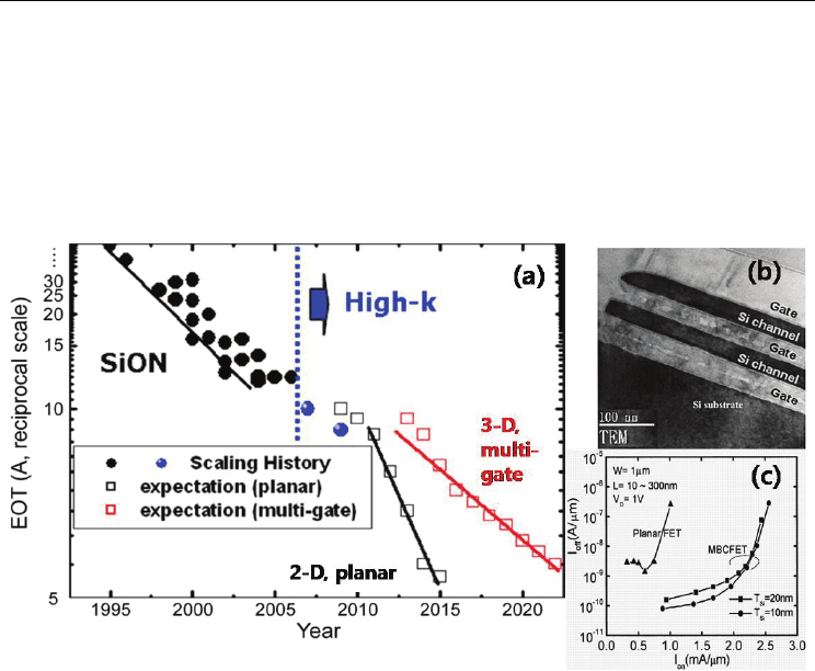
are expected to have the same trend of EOT as those with conventional SiON dielectrics.
This suggests that 3-D structures seem to become essential even with high-
κ
materials. It is
thus believed that developing a 3-D transistor with either a multi-gate or an gate-all-around
structure (Colinge et al, 1990) is quite feasible if one can extend 2-D planar technology to 3-
D. This is because the channel length is no longer restricted by lateral dimension. Figure 5
also shows (b) a cross-sectional TEM (transmission-electron-micrograph) image of one of the
3-D, multi-gate transistors and (c) its Ion-Ioff characteristics are compared with those of 2-D
planar structures.
Fig. 5. (a) Equivalent-oxide-thickness (EOT) scaling trends (Kim, 2010) are shown in
reciprocal scale. Due to the difficulty in controlling the SCE, a sharp decrease in EOT trend
is inevitable for the coming nodes. However, the historical trend can be reverted back in the
case of 3-D, multi-gate transistors. (b) A cross-sectional TEM image of a 3-D, multi-gate and
(c) its Ion-Ioff characteristics are compared with those of the planar (Lee et al., 2003b).
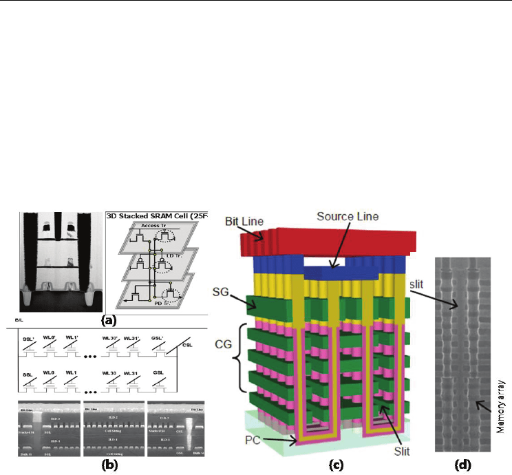
2.2.2 3-D stacking of memory cells
New silicon technology based on 3-D integration has drawn much attention because it
seems to be regarded as one of the practical solutions. Though the concept of 3-D integration
was first proposed in the early 1980’s (Kawamura et al., 1983; Akasaka & Nishimura, 1986),
it has never been thoroughly investigated or verified until now, as neither silicon devices
approached their limits at those times nor high-quality silicon crystal was ready for
fabrication. Recent advances both in selective epitaxial silicon growth at low temperature
(Neudeck et al., 2000) and in high quality layer-transferring technology with high-precision
processing (Kim et al., 2004b), can bring major new momentum to the silicon industry via 3-
D integration technology. The simplicity of memory architecture consisting of memory
array, control logic and periphery logic, makes it relatively easy to stack one-memory cell
array over another. This will ultimately lead to multiple stack designs of many different
memories. Recently, one of the memory manufacturers has started to implement 3-D
integration technology with SRAM to reduce large cell-size (Jung et al., 2004). Figure 6
Ferroelectrics - Applications
130
shows (a) a cross-sectional TEM image of 3-D stacking SRAM (Left) and its schematic
diagram (Right) (Jung et al., 2004): Since transistors stacked onto a given area do not need to
isolate p-well to n-well, SRAM-cell size of 84 F
2
is being reduced to the extremely small cell
size of 25 F
2
. Encouraged by this successful approach, stacked flash memory has also been
pursued. Figure 6 also represents (b) 3-D stacking NAND flash memory (Jung et al., 2006):
This suggests great potential of 3-D memory stacking for large-scale use with 3-D flash-cell
technology, which will spur further growth in high-density applications. Beyond 20 nm
node, we believe that the most plausible way to increase density is to stack the cells
vertically. Figure 6 displays (c) a 3-D schematic view of vertical NAND flash memory
(Katamura et al., 2009), where SG is selecting gate, CG is control gate and PC is pipe
connection. The stacking of memory cells via 3-D technology looms on the horizon, in
particular, for NAND flash memory.
Fig. 6. (a) A cross-sectional TEM image of 3-D stacking SRAM (Left) and its schematic
diagram (Right) (Jung et al., 2004). (b) 3-D stacking NAND flash memory (Jung et al., 2006).
(c) A 3-D schematic view of vertical NAND flash memory (Katsumata et al., 2009), where SG
is selecting gate; CG is control gate; and PC is pipe connection. (d) A cross-sectional SEM
image of memory array after the removal of the sacrificial film (See Katsumata et al., 2009)
It is also believed that logic technology will shift to 3-D integration after a successful
jumpstart in silicon business. The nature of a logic device, where transistors and
interconnections are integrated as key elements, is not much different from those of stacked
memory cells. It may be very advantageous to introduce 3-D integration technology to a
logic area. Note that implementation of interconnection processes seems to be more efficient
in vertical scale. For example, a dual or quad-core CPU can be realized with only a half or
quarter of the chip size, which will result in significantly greater cost-effectiveness. Another
promising use would be to improve logic performance by cutting down on the length of
metallization. Decrease in interconnection length means a huge amount of reduction in
parasitic RC components, i.e., a high speed and power saving. In addition, 3-D technology
will make it easy to combine a memory device and a logic device onto one single chip

Future Memory Technology and Ferroelectric Memory as an Ultimate Memory Solution
131
through hierarchical stacking. Since most parts of SoCs (system-on-chips) in the future will
be allocated to memory, this combining trend will be accelerated. The next step will be to
stack multi-functional electronics such as RF (radio frequency) modules, CISs (CMOS image
sensors) and bio-sensors over the logic and memory layers.
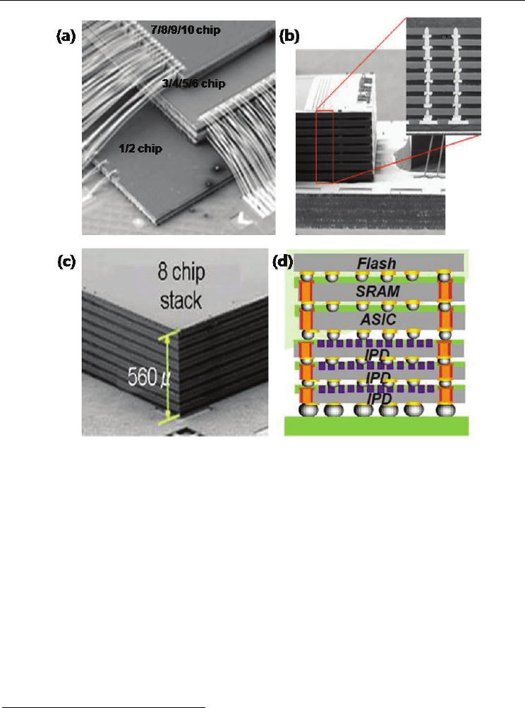
2.2.3 Chip level of 3-D integration
The early version of 3-D integration in chip level has been commercialized already in a
multi-chip package (MCP), where each functional chip (not device) is stacked over one
another and each chip is connected by wire bonding or through the ‘through-via hole’
bonding method within a single package. Figure 7 exhibits (a) a bird’s eyes view of multi-
chip-package (MCP) by wire bonding; (b) wafer-level stack package with through-via-hole;
(c) a photograph of 3-D integrated circuit; and (d) a schematic drawing of a 3-D device for
use in medical applications. The advantages of the MCP are a small footprint and better
performance compared to a discrete chip solution. It is expected that the MCP approach will
continue to evolve. However, the fundamental limitation of MCP will be lack of cost-
effectiveness due to a number of redundancy/repair requirements. In this respect, ‘through-
silicon-via’ (TSV) technology is able to overcome MCP limitations through an easy
implementation of redundancies and repairs. Many groups have reported TSV-based
integrated circuit (TSV IC), where a single integrated circuit is built by stacking silicon
wafers or dies and interconnecting them vertically so that they can function as one single
device (Topol et al., 2006; Arkalgud, 2009; Chen et al., 2009). In doing so, key technologies
include TSV formation, wafer-thinning capability, thin wafer handling, wafers’ backside
processes, and 3D-stacking processes (e.g., die-to-die, die-to-wafer and wafer-to-wafer). In
detail, there are many challenging processes such as etching profiles of TSV sidewall, poor
isolation liners and barrier-deposition profiles. All of these are likely to provoke TSV’s
reliability concerns due to lack of protection from metal (e.g., Cu) contamination. A report of
silicon-based TSV interposers (Rao et al., 2009) may have advantages over traditional PCB or
ceramic substrate in that it has a shorter signal routing. This results from vertical
interconnect and improved reliability due to similarity to silicon-based devices in thermal
expansion and extreme miniaturization in volume. TSV-IC technologies together with the 3-
D interposers will accelerate an adoption of 3-D system-in-package (SiP) with heterogeneous
integration (See Fig. 7d). And this might be a next momentum for genuine 3D IC devices in
the future because of tremendous benefits in footprint, performance, functionality, data
bandwidth, and power. Besides, as the use of 3-D silicon technology has great potential to
migrate today’s IT devices into a wide diversification of multi-functional gadgetry, it can
also stimulate a trend that merges one technology with another, ranging from new materials
through new devices to new concepts. In this regard, new materials may cover the followings:
carbon nano-tube (CNT) (Iijima, 1991), nano-wire (NW) (Yanson et al., 1998), conducting
polymer (Sirringhaus et al. 1998), and molecules (Collier et al., 1999). New devices could
also be comprised of many active elements, such as tunneling transistors (Auer et al., 2001),
spin transistors (Supriyo Datta & Biswajit Das, 1990), molecular transistors (Collier et al.,
1999), single electron transistors (SETs) (Fulton & Dolan, 1987) and others. We may be able
to extend this to new concepts, varying from nano-scale computing (DeHon, 2003) and FET
decoding (Zhong et al., 2003) to lithography-free addressing (DeHon et al., 2003). To a
certain extent, some of these will be readily integrated with 3-D silicon technologies. This
integration will further enrich 3-D silicon technologies to create a variety of new multi-
functional electronics, which will provide further substantive boosts to silicon industry,
allowing us to make a projection of a nano-silicon era into practical realities tomorrow.
Ferroelectrics - Applications
132
Fig. 7. (a) A bird’s eyes view of (a) multi-chip-package (MCP) by wire bonding. (b) Wafer-
level stack package with through-via-hole. (c) A Photograph of 3-D integrated circuit. (d) A
schematic drawing of a 3-D device for medical applications enabled by TSVs and silicon
interposers.
These realities will be manifested in highly desirable applications of combining of information
technology (IT), bio-technology (BT), and nano-technology (NT), to become so called fusion
technology (FT). Given that key obstacles to realize this are tackled by bridging the gap
between previously incompatible platforms in silicon-based CMOS technology and new
technological concepts, a vast number of new applications will unfold. One example may be
many applications related to health sensor technology, in particular, the early recognition of
cancer diseases and the screening of harmful and poisonous elements pervasive in the
environment. Further, when a nano-scale bio-transistor is available, lab-on-a-chip (LoC) will
become a single solution integrating all of its essential components, such as micro-array,
fluidics, sensors, scanners and displayers. Then, by its very nature
8
, one will have tons of
benefits from a mass of disposable LoCs, which will stimulate the future silicon industry.
8
As a successful booster for the silicon industry, whatever will be, it should be a high volume product at
a reasonable price. PCs are high volume products, and hand-held phones are too. In that sense, LoC is
very promising because its potential market is the entire population.

Future Memory Technology and Ferroelectric Memory as an Ultimate Memory Solution
133
2.3 Remarks
Not only do many challenges await silicon industries as technology enters the deep nano-
dimension era but promising opportunities are also there. Equipped with new technologies
such as 3-D scaling and a wealth of new materials, alongside fusing of related technologies,
we will overcome many hurdles ahead and respond technological challenges we will
stumble along the way. All plausible solutions described earlier tell us that planar-based
technology will reach an impassable limit. 3-D technology begins to provide clear signs of
serving as a foundation for a refuel of the silicon industry. The advantages of 3-D
integration are numerous. They include: elimination of uncertainty in the electrical
characteristics of deep nano-scale transistors; extendable use of silicon infrastructures,
especially optical lithography tools; and formation of a baseline for multi-functional
electronics and thus facilitation of implementing a hierarchical architecture, where each
layer is dedicated to a specific functional purpose. Over the next decade, we will see great
endeavors in numerous areas that will greatly stimulate the semiconductor business.
Successful evolutions of device structures will continue and even accelerate at a greater pace
in the not-too-distant future. In addition, device designs will converge onto a single mobile
platform, covering many different capacities and services from telecommunication through
broadcasting and a much higher degree of data processing. In line with this, silicon
technology will still play a critical role in realizing functionally merged solutions. All of
these will permit us to have invaluable clues not just on how to prepare future silicon
technology but also on how to positively influence the entire silicon industry. This will
allow us to attain an even more sophisticated fusing of technologies. As seen in the past,
silicon technology will continue to provide our society with versatile solutions and as-yet
unforeseen benefits in much more cost-effective ways.
3. Ferroelectric memory as an ultimate memory solution
3.1 Introduction
There has been great interest to understand ferroelectric properties from the point of view of
both fundamental physics and the need of nano-scale engineering for memory devices. On
the one hand, since electric hysteresis in Rochelle salt was in 1920 discovered by Valasek
(Valasek, 1921), there have been tremendous efforts to look through ferroelectricity in a
comprehensive way over the past many decades. As a consequence, the phenomenological
theory of ferroelectricity has been presented by many researchers: Devonshire (Devonshire,
1949; Devonshire, 1951); Jona and Shirane (Jona and Shirane, 1962); Fatuzzo and Merz
(Fatuzzo and Merz, 1959); Line and Glass (Line and Glass, 1979); and Haun (Haun, 1988).
The series of their works have been successful to express the internal energy of a
ferroelectric crystal system. This theory has also been examined experimentally in detail,
and extended by Merz (Merz, 1953); by Drougard et. al. (Drougard et al., 1955); and by
Triebwasser (Triebwasser, 1956). Especially, Devonshire’s phenomenological theory
(Devonshire, 1949; Devonshire, 1951) gives the free energy of BaTiO
3
as a function of
polarization and temperature. From this free energy we know what the possible state and
meta-stable states of polarization are in the absence of an applied field. We also know how
polarization changes as a function of field applied to the crystal. In short, according to the
theory, a ferroelectric possesses two minima (e.g., a second-order phase transition) in the
internal energy. These two minima are separated by an energy barrier
Δ
E. Essential feature
of a ferroelectric is that these two minima corresponds to two different spontaneous
Ferroelectrics - Applications
134
polarizations that can be changeable reversibly by an applied field. Under an assumption
that applied electric field is able to surmount the energy barrier, the advent of smart thin-
film technology in evolution of CMOS technology, has enabled to consider a ferroelectric
crystal a useful application. Thinning a ferroelectric film with high purity means that there
could be an opportunity to use ferroelectrics as a memory element.
On the other, integrated ferroelectrics are a subject of considerable research efforts because
of their potential applications as an ultimate memory device due to 3 reasons: First, the
capability of ferroelectric materials to sustain an electrical polarization in the absence of an
applied field, means that integrated ferroelectric capacitors are non-volatile. They can retain
information over a long period of time without a power supply. Second, the similar
architectural configuration of memory cell-array to conventional ones, means that they are
highly capable of processing massive amounts of data. Finally, nano-second speed of domain
switching implies that they are applicable to a high-speed memory device. Since ferroelectric
capacitors was explored for use in memory applications by Kinney et al. (Kinney et al.,
1987); Evans and Womack (Evans & Womack, 1988); and Eaton et al. (Eaton et al., 1988), it
has been attempted to epitomize ferroelectrics to applicable memory solutions in many
aspects. In the beginning of 1990’s, silicon institutes have begun to exploit ferroelectrics as
an application for high-density DRAMs (Moazzami et al., 1992; Ohno et al., 1994). This is
because permittivity of ferroelectrics is so high as to achieve DRAM’s capacitance extremely
high and thus appropriate for high density DRAMs. An early version of non-volatile
ferroelectric RAM (random-access-memory) used to be several kilo bits in packing density.
This lower density (NB. at that moment, DRAM had several ten mega bits in density) is
because of two: One is that its memory unit was relatively large in size, being comprised of
two transistors and two capacitors (2T2C) to maximize sensing signal. The other is that a
ferroelectric capacitor stack has required not only novel metal electrodes such as platinum,
iridium and rhodium, all of which are hard to be fine-patterned due to processing hardness,
but also reluctant metal-oxide materials to conventional CMOS integration due to possible
cross contaminants such as lead zircornate titanate (PbZrTiO
3
) and strontium bismuth
titanate (Sr
1-x
Bi
x
TiO
3
). Next steps for high density non-volatile memory have been
forwarded (Tanabe et al., 1995; Sumi et al., 1995; Song et al., 1999). In similar to DRAM, an
attempt to build smaller unit cell in size was in the late 1990’s that one transistor and one
capacitor (1T1C) per unit memory was developed (Jung et al., 1998). Since then, many
efforts to build high density FRAM have been pursued, leading to several ten mega bits in
density during the 2000s (Lee et al., 1999; Kim et al., 2002; Kang et al., 2006; Hong et al., 2007;
Jung et. al, 2008).
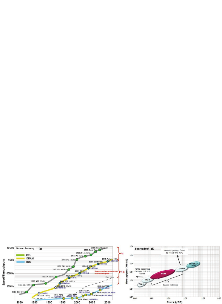
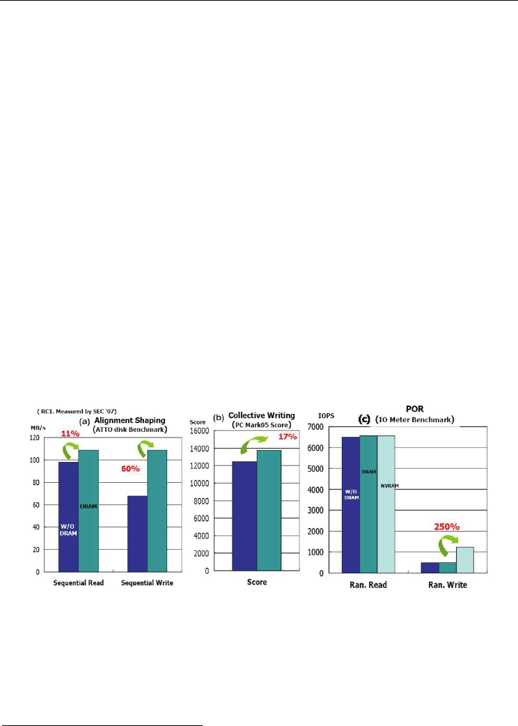
Fig. 8. (a) Evolution of electronic components in data throughput performance. (b) NVM
(non-volatile memory) filling price/performance gap.

Future Memory Technology and Ferroelectric Memory as an Ultimate Memory Solution
135
Among integrated ferroelectrics, one of the most important parameters in FRAM is sensing
signal margin. The sensing signal of FRAM is proportional to remanent polarization (P
r
) of a
ferroelectric capacitor as follows:
∆
2
2
, 10
where A is capacitor’s area; d is capacitor’s thickness. As seen in equation (10), in principle,
we have to compensate the area reduction when technology scales down. However, in
practice, when the thickness of PZT ferroelectric thin film decreases, degradation of
polarization tends to appear in the ferroelectric capacitor due to a dead layer between the
ferroelectric and electrodes (See section 3.3.3). Unlike the requirement of DRAM’s CAT, the
array transistor of FRAM is not necessarily constrained from the off-leakage current due to
no need of the refresh cycles, but from on-current, which is at least greater than several μA
in order for a reasonable read and write speed. Thus, this will greatly relieve technology
scaling quandaries and enable fast technology migration to the high end. This is because
designing of a less leaky cell transistor becomes very difficult in incumbent memories such
as DRAM and NAND/NOR flash due to need of lower doping concentration.
As witnessed in the Moore’s law, there has been enormous improvement in VLSI (very
large-scale integration) technology to implement system performance of computing
platforms in many ways over the past decades. For instance, data throughput of central
processing unit (CPU) has been increased by thousand times faster than that of Intel 286
TM
emerged in the beginning of 1980’s. Alongside, a latest version of DRAM reaches a clock
speed of more than 1 GHz. By contrast, state-of-the-art HDD (hard disk drive) transfers data
at 600 MB/sec around (See Fig. 8a). Note that data rate of the latest HDD is still orders of
magnitude slower than the processor/system-memory clock speed (see Fig. 8b). To achieve
the throughput performance in more effective way, it is therefore needed to bridge
performance gap in between each component. To compensate the gap between CPU and
system memory, a CPU cache
9
has been required and adopted. In line with this, ferroelectric
memory is non-volatile, high-speed. But it has a destructive read-out scheme in core circuitry,
whose memory cells need to return the original state after being read. This is because the
original information is destroyed after read. As a result, it is essential to return the
information back to its original state, which is so-called restore, necessarily following the
read. This operation is so inevitable in the destructive read-out memory such as DRAM and
FRAM. In particular, when the ferroelectric memory are used as one of the storage devices
in computing system, such as a byte-addressable non-volatile (NV)-cache device, the
memory has to ensure lifetime endurance, which is regarded as the number of read/write
(or erase if such operation is required) cycles that memory can withstand before loss of any
of entire bit information. Thus, authors are here trying to attempt not only how FRAM
provides NV-cache solutions in a multimedia storage system such as solid state disk (SSD)
with performance benefits but also what should be satisfied in terms of lifetime data-
retention and endurance in such applications. Here, we also put forward size effect of
ferroelectric film in terms of temperature-dependent dielectric anomaly because a dead
layer plays an adverse role in thickness scaling. In addition, it is very important to ensure
that integration technology of FRAM in nano-dimension is extendable to one of the
9
File system cache is an area of physical memory that stores recently used data as long as possible to
permit access to the data without having read from the disk.
Ferroelectrics - Applications
136
conventional memories. Accordingly, we will present key integration technologies for
ferroelectric memory to become highly mass-productive, highly reliable and highly scalable.
This covers etching technology to provide a fine-patterned cell with less damage from
plasma treatments; stack technology to build a robust ferroelectric cell capacitor;
encapsulation technology to protect the ferroelectric cell capacitors from process integration
afterwards; and vertical conjunction technology onto ferroelectric cell capacitors for multi-
level metallization processes.
3.2 Non-volatile RAM as an ultimate memory solution
SSD, one of the multimedia storage systems, in general, consists of 4 important devices. First
is a micro-controller having a few hundreds of clock speed in MHz, with real-time operating
system (firmware). Second is solid-state storage device such as HDD or NAND flash
memory, which has several hundreds of memory size in gigabyte. Third is host interface
that has the primary function of transferring data between the motherboard and the mass
storage device. In particular, SATA (serial advanced technology attachment) 6G (6
th
generation) offers sustainable 100 MB/s of data disk rate in HDD. In addition, bandwidth
required in DRAM is dominated by the serial I/O (input/output) ports whose maximum
speed can reach 600 MB/s. SATA adapters can communicate over a high-speed serial cable.
Last is a buffer memory playing a considerable role in system performance. As such, DRAM
utilization in SSD brings us many advantages as a buffer memory. For example, in DRAM-
employed SSD, not only does I/O shaping in DRAM allow us to align write-data unit fitted
into NAND flash page/block size but collective write could also be possible. As a result of
sequential write, the former brings a performance benefit improved by 60% at maximum,
and also the latter gives us another performance benefit improved by 17% due to increase in
cache function, as shown in Fig. 9a and b, respectively.
Fig. 9. Impact of DRAM utilization in SSD on system performance. (a) Increase in sequential
read/write by I/O shaping. (b) Performance improvement by collective WRITE. (c)
Additional performance benefit for DRAM plus FRAM in SSD.
As an attempt to implement system performance further, not only does DRAM have been
considered but FRAM has also been taken into account because of its non-volatility and
random accessibility. Before that, it is noteworthy that, in SSD with no NV-cache, system-log
manager is needed to record and maintain log of each transaction
10
in order to ensure that
10
Each set of operations for performing a specific task.
Future Memory Technology and Ferroelectric Memory as an Ultimate Memory Solution
137
file system maintains consistency even during a power-failure. A log file that contains all the
changes in metadata, generally serves as a history list of transactions performed by the file
system over a certain period of time. Once the changes are recorded to this log, the actual
operation is now executed. This is so-called power-off recovery (POR). By contrast, POR is
redundant in FRAM-employed-SSD as a NV-cache because metadata can be protected by
FRAM. Elimination of POR overhead is the single most critical implementation by
utilization of FRAM. This is because FRAM provides such system with byte-addressable
and non-volatile RAM function. Thus, in spite of sudden power failure, system can safely be
protected by adopting FRAM even without POR overhead, ensuring integrity of metadata
stored in the ferroelectric memory. Through many benchmark tools, we have confirmed that
by eliminating this overhead, system performance has been increased by 250% in random
write (See Fig. 9c). This also brings the system to no need of flush operation in file system.
As a consequence, additional 9.4% increase in performance, maximizing cache-hitting ratio.
Since metadata frequently updated do not necessarily go to NAND flash medium,
endurance of the flash memories can be increased by 8% at maximum as well. Besides,
failure rate of operations can be reduced by 20% due to firmware robustness increased
mostly by elimination of the POR overhead.
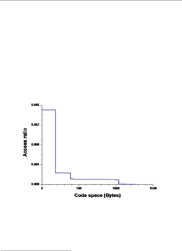
Fig. 10. Data locality of FRAM as a code memory.
Meanwhile, how many endurance cycles are necessary for use in applications of NV-cache
solutions such as data memory and code memory? To answer this question, we need to
understand access patterns of NV-cache devices in multimedia system. Now, we take into
account the followings: First is the ratio of read/write per cycle in data memory (likewise,
number of data fetching per cycle in code memory). Generally, the ratio for data memory
and code memory is 1.00 and 0.75, respectively. Second is data locality
11
. Figure 10 is a
simulation result showing strong locality of 1.5% when FRAM has been considered a code
11
The locality of reference is the phenomenon that the collection of data locations often consists of
relatively well predictable clusters of code space in bytes.
Ferroelectrics - Applications
138
memory. As shown in Fig. 10, less than 200 bytes of code space is more frequently accessed.
Provided wear-leveling in read/write against the strong locality and taking an example of
20 MHz clock frequency of main memory (CPU clock ~ 200 MHz), what has been found is
that the endurance cycles for 10-year lifetime becomes less than 9.5 × 10
13
. This number of
cycles is far less than the cycles we presumably assumed, which is more than 10
15
cycles.
Thus, authors believe that more than 1.0 × 10
14
of the endurance cycles is big enough to
ensure that the ferroelectric memory as a NV-cache is so endurance-free as to be adopted to
a multimedia storage system.
3.3 Reliabilities
3.3.1 Retention
Since Merz’s exploration of domain switching kinetics in the mid 1950’s (Merz, 1954), it is now
believed that polarization reversal occurs in a way of domain nucleation and growth
(Landauer, 1957; Pulavari & Kluebler, 1958; Key & Dunn, 1962; Du & Chen, 1997; Jung et al.,
2002; Kim et al., 2005; Jo et al., 2006). The retention time of FRAM is closely related to a decay
rate of the polarization reversal of a ferroelectric capacitor as expressed in formula (11).
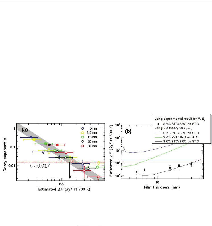
Fig. 11. (a) A decay exponent n plot against estimated thermal energy
Δ
F
*
/k
B
T in various
thickness of of BaTiO
3
films and (b) thermal energy barrier
Δ
F
*
/k
B
T as a function of thickness
in different ferroelectric stacks.
11
∆
2
12
where P
0
is initial remanent polarization; P(t) is remanent polarization at time t; t
0
is a time
constant; n is an exponent; ∆
is domain free energy; E is homogeneous electric field
applied externally; V is the volume of domain nucleus;
σ
w
is domain wall energy; A is
domain wall area. While the first term of Eq. (12) represents the electrostatic energy gained
by formation of a domain nucleus, the second is the surface energy, and the last term is the
field energy of the depolarizing field (Merz, 1954). Provided that length of domain nuclei is
much smaller than thickness of a ferroelectric, half-prolate spheroidal nuclei tends to be
formed and finally reaches a cylindrical shape (Key & Dunn, 1962; Jung et al., 2002). Under
such an assumption, if one can measure depolarization energy of Eq. (12), we can now