Lallart M. Ferroelectrics: Applications
Подождите немного. Документ загружается.


Future Memory Technology and Ferroelectric Memory as an Ultimate Memory Solution
139
estimate ∆
/
, where k
B
is Boltzmann constant. Based on experimental values of
depolarization field E
d
that ranges from 300 to 800 kV/cm (Kim et al., 2005), the
corresponding ∆
/
is estimated to 4 to 20 at ambient temperature (Jo et al., 2006).
Figure 11 represents (a) a decay exponent n plot against estimated thermal energy
Δ
F
*
/k
B
T in
various thickness of BaTiO
3
films and (b) thermal energy barrier
Δ
F
*
/k
B
T as a function of
thickness in different ferroelectric stacks. As seen in Fig. 11a, in most of interesting nano-
ferroelectrics with thickness ranging from 5 to 30 nm, the energy barrier is evaluated to
Δ
F
*
/k
B
T ~ 150 k
B
T for n ~ 0.017, which is the exponent corresponding to 50% of polarization
decay during 10 years in Eq. (11). Thus, as shown in Fig. 11b, if one takes into account a
stack of SrRuO
3
-PbTiO
3
-SrRuO
3
(SRO-PTO-SRO), the energy barrier of polarization reversal
via the formation of domain nuclei during 10 years is more than 150 k
B
T, which means that
there is virtually no retention conumdrum in FRAM as long as a ferroelectric stack is
properly chosen.
3.3.2 Endurance
In FRAM, it is not readily achieved to assure whether or not a memory device can endure
virtually infinite read/write cycles. This is because of memory size that is several tens or
hundreds megabits typically. For instance, a HTOL (high temperature operational life) test
during 2 weeks at 125
o
C, is merely a few millions of endurance cycles for each memory cell
in 64-Mb memory size, for example. Even taking into account minimum number of cells (in
this case 128 bits because of 16 I/Os), time to take evaluation of 10
13
cycles is at least more
than 20 days. Therefore, it is essential to find acceleration factors to estimate device
endurance through measurable quantities such as voltage and temperature. However, direct
extraction of acceleration factors from memory chips is not as easy in practice as it seems to
be in theory. This is because VLSI circuit consists of many discrete CMOS components that
have a temperature and voltage range to work. Generally, more than 125
o
C is supposed to
be a limit to operate properly. A voltage range of a memory device is also specified in given
technology node (±10% of V
DD
=1.8 V in this case). Despite those difficulties, it has been
attempted to figure out acceleration factors in terms of temperature and voltage, together
with information obtained from capacitor-level tests.
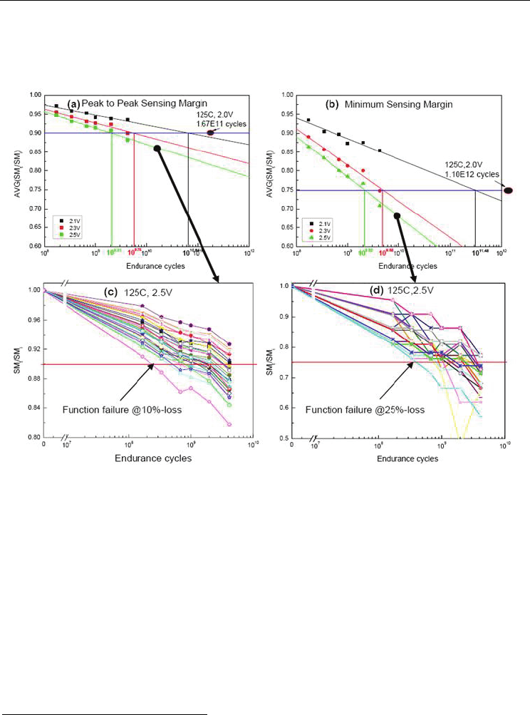
In regard to package-level endurance, figure 12 represents changes in (a) peak-to-peak
sensing margin (SMpp) and (b) tail-to-tail sensing margin (SMtt) as read/write cycles
continues to stress devices cumulatively at 125
o
C. Both SMpp and SMtt have been obtained
by averaging out 30 package samples for each stress voltage. Function-failed packages have
been observed when SMpp and SMtt reach 10% and 25% loss of each initial value,
respectively. As seen in Fig. 12a and b, voltage acceleration factors (AF
V
) between 2.0 V and
2.5 V has been calculated by these criteria (AF
V
= 81 at SMpp and AF
V
= 665 at SMtt). In
other words, the test FRAMs can endure 1 × 10
12
of read/write cycles at the condition of 125
o
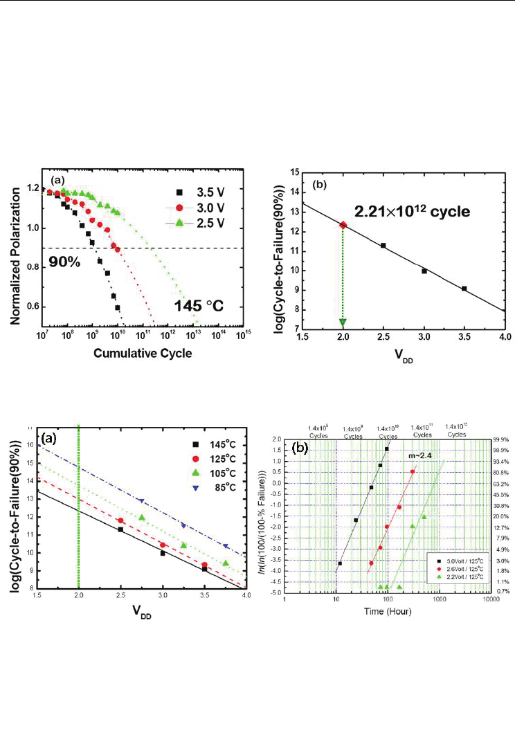
C and 2.0 V. Second, in capacitor-level endurance, figure 13 is (a) a normalized polarization
plot against cumulative fatigue cycles at 145
o
C in a variable voltage range and (b) a
logarithm plot of cycle-to-failure (CTF) as a function of stress voltage in a various range of
temperature. Here, we introduce a term of CTF which is referred to as an endurance cycle at
which remanent polarization (or sensing margin) has a reasonable value for cell capacitors
(or memory) to operate. Polarization drops gradually as fatigue cycles increase and the
collapsing rate is accelerated as stress voltage goes higher. Likewise, provided 10% loss of
polarization is criteria of CTF, the CTF at 145
o
C and 2.0 V approximates 2.2 × 10
12
. (NB. This
Ferroelectrics - Applications
140
is reasonable because samples of 10% loss in SMpp turned out to be defective functionally.)
Considering temperature- and voltage-acceleration factors from Fig. 13a, acceleration
condition of 145
o
C, 3.5V is more stressful in 5 orders of magnitude than that of 85
o
C, 2.0 V.
In other words, 1.0 × 10
9
of CTF at 145
o
C, 3.5 V is equivalent to 6.0 × 10
14
at 85
o
C, 2.0 V.
Fig. 12. Changes in (a) peak-to-peak sensing margin (SMpp) and (b) tail-to-tail sensing
margin (SMtt) as a function of endurance cycles at 125
o
C. (c) SMpp vs. endurance cycles at
125
o
C, 2.5 V. (d) SMtt vs. endurance cycles at 125
o
C, 2.5 V. SMt and SMi of the ordinate in
Fig. 12a and b is sensing margin at time t and initial time, respectively.
Results of the acceleration factors obtained from device-level tests differ from those in
capacitor-level. For example, while AF
V
(2.5 V/2.0 V) of 81
in device-level tests
12
, that of 16 in
capacitor-level. We have yet to find a reasonable clue of what makes this difference. But it
could be thought that the difference might arise from the fact that a memory device contains
many different functional circuitries such as voltage-latch sense amplifiers, word-line/plate-
line drivers, all of which make tiny amount of voltage difference magnify each effect on cell
capacitors. This tendency can also be observed in the big gap of AF
V
obtained from two
different definitions between SMtt (AF
V
= 665) and SMpp (AF
V
= 81). Tail-bit behaviors of
memory cells could include a certain amount of extrinsic imperfection, in general. Thus, we
believe that results tested in capacitor-level seem to be close to a fundamental nature of CTF
12
It is thought that AFV in capacitor-level tests follows AFV of SMpp in device-level rather than that of
SMtt because of nature of capacitor-level tests that average out all the cell capacitor connected in
parallel.
Future Memory Technology and Ferroelectric Memory as an Ultimate Memory Solution
141
than those in device-level tests due to lack of extrinsic components. Figure 14 is (a) a
logarithm plot of CTF as stress voltage increases in a various range of temperature and (b)
Weibull distribution of endurance life in package samples tested at 125
o
C in a various
voltage range. The distributions in a 2.2-3.0 V range of voltage have a similar shape
parameter, m~2.4. This suggests that evaluation of endurance tests in device-level makes
sense in physical term. As seen in Fig. 14a, voltage-endurance stress at less than 2.0 V does
not allow us to obtain any sign of degradation in sensing margins within a measurable time
span. Nor does temperature-endurance stress above 125
o
C due to off-limits of operational
specifications of the device.
Fig. 13. (a) A normalized polarization plot against cumulative fatigue cycles at 145
o
C in a
variable voltage range. (b) Logarithm of CTF vs. stress voltage, V
DD
at 145
o
C.
Fig. 14. (a) A logarithm plot of CTF as stress voltage increases in a various range of
temperature and (b) distributions of endurance life in device-level tests at 125
o
C.
3.3.3 Temperature-dependent dielectric anomaly
Since ferroelectricity involves the cooperative alignment of electric dipoles responding
external field applied, there should be a critical volume below which the total energy
associated with domain nucleation and growth, is outweighed by the entropic desire to
Ferroelectrics - Applications
142
disorder. There has been a trend in recent literature to use the term “size effect” relating to
the stability of spontaneous polarization to specifically describe the manner in which
reduced size leads to progressive collapse of ferroelectricity (Saad et al., 2006). Finding the
point at which this size-driven phase transition occurs is obviously interesting and
fundamentally important, and thus various groups have done excellent works to elucidate,
via both theory (Li et al., 2996; Junquera & Ghosez, 2003) and experiment (Streiffer et al.,
2002; Tybell et al., 1999; Nagarajan et al., 2004), the dimensions at which ferroelectricity is
lost. In that sense, one of the most critical quantities in ferroelectrics is remanent polarization
P
r
, which can be expressed as below:
, 13
and
1
1
χ
2
2
, 14
where P
S
is spontaneous polarization;
α
and
β
are standard bulk LGD (Landau-Ginzburg-
Devonshire) coefficients, provided that ferroelectric materials have a second-order phase
transition while neglecting the P
6
terms due to lack of contribution in the free energy
expansion of the LGD theory (then, a hysteresis loop would be a cubic equation);
χ
is the
dielectric susceptibility; T
C
is the transition temperature; and C is the Curie constant. As
denoted in Eq. (10) and (13), the sensing signal depends strongly on spontaneous
polarization P
S
, which is also varying material constants such as and . Eq. (14) is
temperature-dependent dielectric anomaly, so-called, the Curie-Weiss law. Thus, in this
section, we will examine whether or not size effect of ferroelectrics is intrinsic.
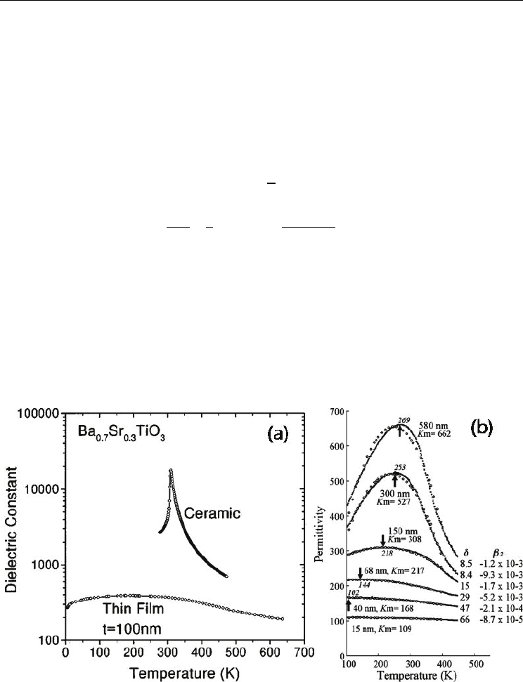
Fig. 15. Changes in dielectric constants as a function of temperature in BST materials: (a)
Comparison of temperature-dependent dielectric constants between a ceramic bulk and a
film 100-nm thick (Shaw et al., 1999). (b) Variation of relative permittivity as a function of
temperature with a variety of thickness ranging from 15 to 580 nm (Parker et al., 2002)
Future Memory Technology and Ferroelectric Memory as an Ultimate Memory Solution
143
In many ferroelectrics, ferroelectric phenomena could be ascribed to a dielectric origin, so-
called, temperature dependent dielectric anomaly (Wieder, 1958; Pulavari & Kluebler, 1958).
Since most integrated ferroelectrics are embedded as a thin film, it is desirable to pay much
attention to the temperature-dependent dielectric properties in thin-film ferroelectrics. In
this regard, there have recently been good approaches to evaluate size effects of
ferroelectrics on their dielectric behaviors, in particular, in terms of temperature
dependence. Figure 15 shows changes in the dielectric constant as a function of temperature
in Ba
0.7
Sr
0.3
TiO
3
(BST) materials. As seen in Fig. 15a, Shaw et al. (Shaw et al., 1999) observed
that temperature-dependent dielectric constant in a Ba
0.7
Sr
0.3
TiO
3
bulk ceramic undergoes
sudden change in value i.e., a first-order transition near ambient temperature at which a
peak of dielectric constant in thin-film Ba
0.7
Sr
0.3
TiO
3
100 nm thick, suffers a collapse of
dielectric constant by orders of magnitude with severe broadening of Curie anomaly. This
suggests a second-order transition. Along with the observation of Shaw et al., Parker et al.
(Parker et al., 2002) measured variations of dielectric constant as a function of temperature
over a variety of thickness ranging from 15 to 580 nm for Ba
0.7
Sr
0.3
TiO
3
. They found that the
temperature dependence of the dielectric constant exhibits diffusive shapes, also suggesting
second-order transitions shown in Fig. 15b. They also found that the temperature maxima in
the relative permittivity plots tend to decrease as the film thickness decreases, implying
reduction of the transition temperature, T
C
.
Fig. 16. (a) A relative permittivity plot as a function of temperature in BaTiO
3
of single crystal
with a variety of thickness that ranges from 447 to 77 nm. (b) The inverse of relative
permittivity plot as a function of temperature in BaTiO
3
crystal 77-nm thick (Saad et al., 2006).
There are many possible origins to explain these temperature-dependent dielectric
properties: First, these effects could arise from an intrinsic size effect that results in a drop in
permittivity with decreasing sample dimension. Second is a model suggesting that a dead
layer of grain boundary in BST films could have a low permittivity value compared to that
of their grain interior; although the microstructure in the films has a columnar shape,
resulting in a parallel rather than series capacitance contribution. Third, this is because of
structural imperfection at film-electrode interfaces, consisting of interfacial dead layers and
the biaxial strain caused by the thermal expansion mismatch with the substrate (Shaw et al.,
1999; Parker et al., 2002). It is necessary to know whether the first case weights less severely

Ferroelectrics - Applications
144
than the others, because the first is instrinsic. In this respect, Saad et al. (Saad et al., 2004a,
2004b) devised a method to thin bulk single-crystal BaTiO
3
using a focused ion beam (FIB)
in order to evaluate the size effects of single crystal ferroelectrics thus excluding grain
boundaries. The dielectric behaviors as a function of temperature in BaTiO
3
single crystals
has been evaluated with a range of thickness from 447 nm to 77 nm (Morrison et al., 2005),
fabricated from a bulk single crystal BaTiO
3
. Figure 16 shows (a) a relative permittivity plot
as a function of temperature in these single crystals of BaTiO
3
and (b) the reciprocal relative
permittivity plot of the 77 nm BaTiO
3
as a function of temperature. Startlingly, dielectric
constants have similar behavior to that of bulk BaTiO
3
single crystal even down to 77 nm
thick. The dielectric constant in BaTiO
3
77 nm thick gradually decrease over a range from
2,738 to 2,478 at temperature corresponding to 300 to 365 K, considerably increases and
abruptly soars up to 26,663 at 410 K. The dielectric constant reaches a peak of 26,910 at 413 K
and hyperbolically dcreases as temperature increases further.
In general, the dielectric constant in bulk BaTiO
3
single crystal are regarded as 160 for
c
(parallel to the polar axis) and 4100 for
a
(normal to the polar axis) at ambient temperature
(Landauer et al., 1956; Benedict & Duran, 1958). In addition, the sudden change in dielectric
constants due to the phase transition from FT (ferroelectric, tetragonal) to PC (paraelectric,
cubic), occurs either 122
o
C upon heating or at 120
o
C on cooling (Merz, 1953; Drougard &
Young, 1954). In Fig. 16a, the transition temperature T
C
is a little bit different from one of
bulk BaTiO
3
.
13
Morrison et al. (Morrison et al., 2005), however, think that this difference may
be caused by the fact that the temperature of thermocouple placed on a heater block is a
little bit higher than that on the sample. Thus, considering the temperature artefact, the
abrupt change in dielectric constant occurs at a temperature close to that observed in bulk
BaTiO
3
. Alongside the dielectric constant as a function of temperature, the inverse of the
dielectric constant as a function of temperature is shown in Fig. 16b for the 77-nm BaTiO
3
single crystal. According to the Curie-Weiss law, the Curie-Weiss temperature T
0
can also be
estimated at 382 K from the extrapolation as shown in Fig. 16b. As a result, for the 77-nm
BaTiO
3
single crystal, they can obtain that the difference
Δ
Temp between T
C
and T
0
is
approximately 13
o
C, which is quite good aggreeement wth experimental results obtained
from bulk BaTiO
3
single crystal, in which
Δ
Temp = 14
o
C (Merz, 1953; Drougard & Young,
1954). These results provide a very intersesting and promising clue, because ferroelectric
properties even in 77-nm thickness are expected to show a similar dielectric behavior with
that of bulk BaTiO
3
. In addition, the first-order transition from FT to PC in ferroelectrics can
appropriately be decribed by the dielectric behaviors near the transition temepertures. They
conclude therefore that, down to 77 nm dimension, the intrinsic size effect has negligible
influence on the temperature-dependent dielectric properties. Moreover, it is not difficult to
estimate the Curie constant C from the Curie-Weiss plot because the 77-nm sample of BaTiO
3
exactly follows the typical Curie-Weiss law as shown in Fig. 16b. From the slope of 1/
r
vs.
T, the Curie constant is approximately 4.53 × 10
5
o
C, which is compared to experimental
values of 1.56 × 10
5
and 1.73 × 10
5
o
C, obtained by Merz (Merz, 1953) and Drougard and
Young (Drougard & Young, 1954), respectively. The Curie constant is in the same order of
magnitude but is roughly 3 times larger than those compared. This may be because of two
13
It was widely accepted that the Curie point of undoped crystal and ceramic BaTiO
3
was near 120 ºC.
Measurements on highly purified ceramics and on crystals grown by Remica’s process (Remica &
Morrison Jackson, 1954) but without the addition of Fe
3+
have shown that their Curies temperature is
near 130 ºC (Jaffe et al., 1971).
Future Memory Technology and Ferroelectric Memory as an Ultimate Memory Solution
145
factors: Errors in electrode area and thickness can affect the Curie constant dramatically; and
the temperature difference between sample and thermocouple may not be constant.
3.4 Key technologies
Etching damage: It is widely accepted that as a device shrinks, node separation of cell
capacitors is not readily achievable due to necessity of novel metals that served as electrodes
of the MIM (Metal-Insulaor-Metal) cell capacitor, such as iridium, iridium oxide, strontium
ruthenium oxide (SrRuO
3
). In typical, remanent polarization depends heavily on processing
temperature at which ferroelectric PZT (PbZr
0.4
Ti
0.6
O
3
) is etched. The remanent polarization
(P
r
) value drops drastically as temperature of the processing chuck in an etching chamber
increases. According to a report of etching impact on ferroelectrics (Jung et al., 2007), there is
no direct evidence how higher-temperature etching makes a P
r
value smaller. But it is
believed that a certain amount of halides or halide ions might accelerate chemical reduction
during the etching process at higher temperature, in particular, at the interfaces of the cell
capacitors. Thus, Jung et al. (Jung et al., 2007) reported that ferroelectric cell-capacitors
suffering a severe etching damage, are likely to follow bulk-limited conduction such as
space-charge-limited current (SCLC), rather than those of electrode-limited.
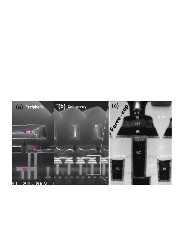
Fig. 17. Cross-sectional micrographs both (a) in a peripheral circuitry region and (b) in a cell
region, (c) in which one of the cell capacitors is pictured (Jung et al., 2008).
Stack technology: Building a stack for a robust ferroelectric cell capacitor is a more important
part of the entire integration than any other process due to the fact that the preparation of a
ferroelectric thin-film plays a crucial role in whether the cell capacitors have the ferroelectric
properties in a certain level of integration. For example, Qos-retention charge of a sol-gel
derived PZT film is severely degraded if one evaluates non-volatile polarization by using
the two-capacitor measurement technique
14
. This tells us how a ferroelectric film is
14
Qos-retention means opposite-state charge retention that is change in non-volatile polarization values
elapsed after a certain amount of time and temperature stress, before which the two capacitors are written
to data 1 (D1) and data 0 (D0). In general, the Qos-retention has a faster decay rate than
Qss-retention
(same-state charge retention) does under the same acceleration condition because imprint change has a
much more severe impact on degradation of non-volatile polarization than depolarization increases.
Ferroelectrics - Applications
146
vulnerable to loss of ferroelectricity when film preparation is poor. The memory device
integrated with CVD (chemical vapor deposition)-derived PZT film has twice bigger sensing
margin than that the sol-gel-based device has even after severe suffering of a thermal
acceleration test during 1000 hours at 150
o
C. In addition, it is also important to regulate
deposition temperature in CVD preparation of PZT films. SMpp of FRAM with the PZT film
prepared at adequate temperature is more than 650 mV, otherwise FRAM with a less
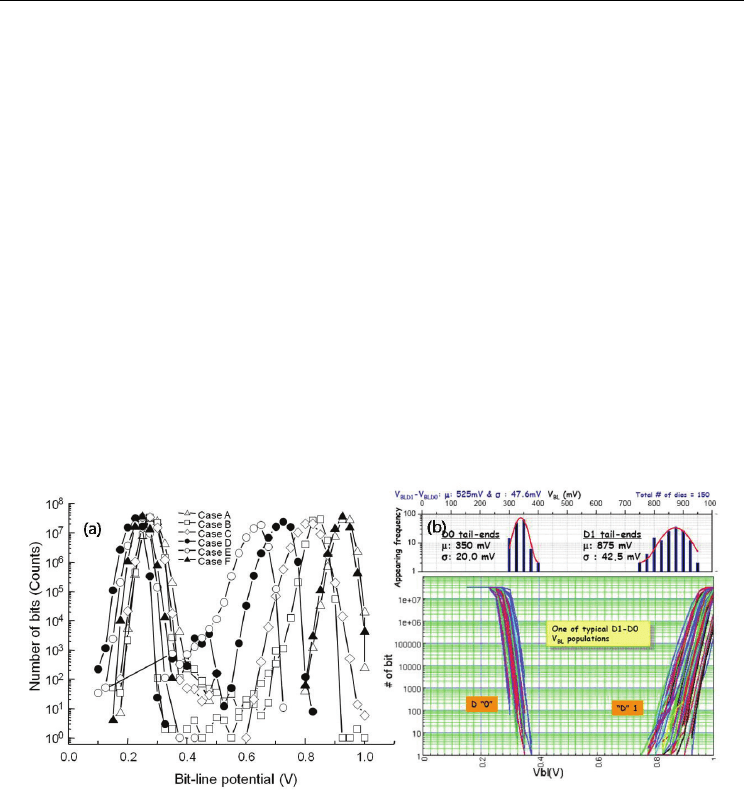
optimized PZT film has SMpp less than 550 mV (See Fig. 18).
Integration technologies
Case A Case B Case C Case D Case E Case F
Etching temperature
Low High Low High High Low
PZT deposition
Regulated Regulated Not Regulated Regulated Regulated
Capping thickness
Thick Thick Thick Thick Thin Thick
Recovery Anneal
No anneal No anneal No anneal No anneal No anneal Anneal
Table 2. A list of combination of different integration conditions.
Encapsulation Technology: In general, ferroelectric capacitors comprise a perovskite-oxide-
based ferroelectric film and novel metals that have a catalytic effect on oxide layers. The
metallic electrodes of the ferroelectric capacitors consist of top-electrode (TE) SRO
underneath iridium and bottom-electrode (BE) iridium. Due to these novel metals, oxide of
the perovskite ferroelectric is very prone to chemical reduction during many hydrogen-
based processes such as interlayer dielectrics (ILD) and inter-metallic dielectrics (IMD).
Thus, it is essential for protecting the capacitors from these integration processes in order to
build a robust capacitor. Thus, a ferroelectric cell capacitor seems to be capped with Al
2
O
3
that needs to be deposited conformally on its sidewall. The Al
2
O
3
layer is, typically,
prepared by an atomic-layer-deposition (ALD) method. By opting a thicker Al
2
O
3
layer, one
can have not only a sharper distribution of bit-line potential but 33% increase in SMpp as
well, compared with the case of an Al
2
O
3
layer thinner.
Vertical conjunction: FRAM has similar architecture with one of the DRAMs, featured by
folded bit-line and voltage-latch sense amplifiers. But a prominent difference between
FRAM and DRAM is, in architecture, how to form the plate node of a cell capacitor−the
other end is connected to the storage node of a cell transistor in both DRAM and FRAM.
While a bunch of plate nodes in DRAM is connected together, a few plate nodes in FRAM
should be separated. The reason of the separation is to give a plate pulse independently to
each plate line. Due to this essential contact between cell capacitors and the plate lines,
metallization in FRAM needs a special care in integration. This is because contact forming
onto the top electrode of a cell capacitor may provoke another root-cause of capacitor
degradation during the process integration. Since it is suitable for protecting ferroelectric
capacitors from any involvement of aluminum when forming the plate line and strapping
line, an addition-top-electrode (ATE) scheme has been adopted for this contact formation
(Kim et al., 2002). The ATE landing pad consists of iridium oxide and iridium. Through a
proper anneal process, what has been achieved is to decrease data 0 population of bit-line
potential as low as possible, so that 8% improvement in SMpp is attainted.
Figure 18 summarizes (a) populations of bit-line potential as integration differently applied
and (b) tail-bit populations of V
BLD1
and V
BLD0
for the integration scheme of the case F in
table 2. The number of dies is 150 in total. Table 2 also summaries how each integration
technology to combine. The overall population of bit-line potential has a strong impact on
changes in data 1 distribution when each technology varies as shown in table 2. First,
Future Memory Technology and Ferroelectric Memory as an Ultimate Memory Solution
147
imperfect encapsulation of the cell capacitor causes bit distribution to become wider and
bigger loss of the peak value in data 1 that corresponds to switching charge quantity in
ferroelectric cell capacitors. This charge lessening effect may be accelerated under the severe
etching condition, for example, etching at high temperature. That is why the case E shows
the smallest bit-line distribution in Fig. 18a in spite of the fact that the PZT thin film is
properly deposited at a regulated condition. Second, when one applies a poorly regulated
deposition condition to a ferroelectric thin-film preparation, broadness of cell-charge
distribution appears dominantly as seen in the case C of Fig. 18a. Third, etching of
ferroelectric capacitors in highly reduced ambient could result in tailing of data 1
distribution, giving rise to a certain loss of sensing margin as seen in the case B of Fig. 18a.
Last, the contact formation onto the top electrode of cell capacitors should be emphasized
because it might have an advantageous effect in the distribution of data 0 not only on
lessening of the peak value but on being sharp without any loss of the data 1 distribution, as
shown in the case F of Fig. 8a. Through the combination of key integration technologies, 525
mV of SMtt in sensing margin has been achieved (Jung et al., 2007). To recapitulate it,
preparation of ferroelectric capacitors is very important to realize highly reliable and
scalable FRAM. But all the integration technologies followed by the capacitor stacking is
equally important, in particular, in a smaller dimension. This is because nano-scaled
ferroelectric capacitors are so vulnerable as to lose the ferroelectric properties during ever-
growing integration processes as reported here.
Fig. 18. (a) Data 1/Data 0 distributions of bit-line potential as integration technology varies
from case A to F (See Table. 2). (b) Tail-bit populations of V
BLD1
and V
BLD0
for an integration
scheme in table 2. The number of dies is 150 in total.
3.5 Conclusions
Utilization of FRAM as a NV-cache solution in a multimedia storage system such as SSD,
gives users critical advantages. By elimination of POR overhead due to its non-volatility,
random-write throughput can be enhanced by more than twice. In spite of strong data
locality of FRAM, 10-year lifetime endurance has been estimated to be less than 1.0 × 10
14
cycles in such system. This endurance is much less than that we presume (e.g., ~10
15
due to
every-time access for 10 years). From the investigation of acceleration factors both in device-
level and in capacitor-level, CTF of the FRAM evaluated has been estimated to

Ferroelectrics - Applications
148
approximately 6.0 × 10
14
at a system operating condition. To be in a nutshell, ferroelectric
memory as a NV-cache seems to be a very plausible scenario for increase in data throughput
performance of SSD. In assertion of endurance, lifetime endurance is no longer problematic
even in the FRAM based on a destructive read-out scheme. On top of that, the introduction
of ferroelectric materials to conventional CMOS technologies has brought us to realize non-
volatile, byte-addressable and high-speed memory. This is thanks not only to bi-stable states
of a ferroelectric but also to tremendous efforts done by many institutes around the world,
trying to epitomize it in two folds. One is, mostly done by silicon institutes, development of
thin-film technology with high precision and high purity for a ferroelectric cell capacitor.
The other is, mainly pursued by academia, to scrutinize thin-film ferroelectrics for whether
or not their intrinsic properties (e.g., order parameters) are restricted by scaling of
capacitor’s thickness, so-called size effect. What both found is that ferroelectric properties is
not restricted by scaling of thin ferroelectrics, at least within a concerned integration range
of thickness, e.g., less than 10 unit perovskite-cells in polar axis are enough to have stable
minima in dipole energy. Note that lattice constant of ferroelectrics is several Angstroms.
Also, what they found is that a dead layer is not fundamental one in extremely thin
ferroelectric capacitors. This suggests that gigabit density NV-RAMs by using ferroelectrics
will be in the market place in the future, under an assumption that FRAM follows DRAM’s
approach to build ferroelectric cell capacitors in a 3-D way. Such assumption is not an
illusion because physical thickness of storage dielectrics in state-of-the-art DRAM, is several
ten Angstroms.
4. References
Akasaka, Y & Nishimura, T. (1986). Concept and Basic Technologies for 3D IC Structure,
Electron Devices Meeting, IEDM Technical Digest. IEEE International, (December
1986), pp.488-492
Arkalgud, S. (2009). Leading edge 3D technology for high volume manufacturing, Dig. Tech.
Papers, VLSI Technology Symposium, (June 2009), pp. 68-69, 978-1-4244-3308-7
Auer, U.; Prost, W.; Agethen, M.; Tegude, F.-J.; Duschl, R. & Eberl, K. (2001). Low-voltage
mobile logic module based on Si/SiGe interband tunneling devices,” IEEE Electron
Dev. Lett., Vol. 22, (May 2001), pp.215-217, ISSN 0741-3106
Benedict, T. & Duran, J. (1958). Polarization Reversal in the Barium Titanate Hysteresis
Loop, Phys. Rev. Vol. 109, (February 1958), pp. 1091-1093
Byeon, D.; Lee, S.; Lim, Y.; Park, J.; Han, W.; Kwak, P.; Kim, D.; Chae, D.; Moon, S.; Lee, S.;
Cho, H.; Lee, J.; Kim, M.; Yang, J.; Park, Y.; Bae, D.; Choi, J.; Hur, S. & Suh, K.
(2005). An 8 Gb multi-level NAND flash memory with 63 nm STI CMOS process
technology, Solid-State Circuits Conference, 2005. Digest of Technical Papers. ISSCC.
2005 IEEE International, (February 2005), Vol. 1, pp. 46-47, ISBN 0-7803-8904-2
Chau, R.; Doyle, B.; Kavalieros, J.; Barlage, D.; Murthy, A.; Doczy, M.; Arghavani, R. &
Datta, S. (2002). Advanced Depleted-Substrate Transistors: Single-gate, Double-
gate and Tri-gate, Technical Digest, International Conference on Solid State Devices and
Materials (SSDM), (August 2002), pp. 68-69
Chen, D.; Chiou, W.; Chen, M.; Wang, T.; Ching, K.; Tu, H.; Wu, W.; Yu, C.; Yang, K.; Chang,
H.; Tseng, M.; Hsiao, C.; Lu, Y.; Hu, H.; Lin, Y.; Hsu, C.; Shue, W. & Yu, C. (2009).