Leroy C., Rancoita P.-G. Principles Of Radiation Interaction In Matter And Detection
Подождите немного. Документ загружается.

January 9, 2009 10:21 World Scientific Book - 9.75in x 6.5in ws-bo ok975x65˙n˙2nd˙Ed
280 Principles of Radiation Interaction in Matter and Detection
3.3.3 Longitudinal and Lateral Hadronic Development
The hadronic cascade, similarly to the electromagnetic cascade, develops along the
incoming particle direction (longitudinal direction) as long as the produced secon-
daries have enough energy to continue the multiplication process. Hadronic cascades
were experimentally studied in different materials and for a wide range of incoming-
particle energies [Friend et al. (1976); Cheshire et al. (1977); Holder et al. (1978);
Sessom et al. (1979); Amaldi (1981); Bock et al. (1981); Della Negra (1981); Mu-
raki et al. (1984); Fabjan (1986); Catanesi et al. (1987); Leroy, Sirois and Wigmans
(1986); SICAPO Collab. (1991b, 1993a)].
In the following, we will express the longitudinal shower depth t in units of
interaction lengths λ
A
[Eq. (3.76)].
To a first approximation, the 95% longitudinal containment of hadronic-shower
cascades, L
95%
, which corresponds to the absorber depth within which 95% of the
hadronic-cascade energy will be deposited (on average), is given by [Fabjan (1986)]:
L
95%
≈ t
max
+ 2.5λ
a
, (3.78)
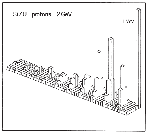
Fig. 3.27 Measured visible-energy for 12 GeV protons as a function of the U calorimeter depth and
the strip location (reprinted with permission from Borchi, E. et al., Evidence for compensation
and study of lateral shower development in Si/U hadron calorimeters, IEEE Transactions on
Nuclear Science, Volume 38, Issue 2, Apr. 1991, pages 403–407, doi: 10.1109/23.289333,
c
° 1991,
IEEE, e.g., for the list of the authors see [SICAPO Collab. (1991b)]; see also [Leroy and Rancoita
(2000)]). The depleted width of the silicon detectors is ≈ 200 µm. Each strip is, on average, 36 cm
long and 4 cm wide. The total U depth is 50 cm and the lateral coverage is 28 cm.
January 9, 2009 10:21 World Scientific Book - 9.75in x 6.5in ws-bo ok975x65˙n˙2nd˙Ed
Nuclear Interactions in Matter 281
where
t
max
≈ 0.2 ln[E(GeV)] + 0.7
is the cascade maximum-depth; λ
a
(in units of λ
A
) describ es the exponential decay
of the cascade beyond t
max
and varies with the energy as [Fabjan (1986)]
λ
a
= [E(GeV)]
0.13
.
Equation (3.78) (for L
95%
) describes the data available in the energy range of a
few GeV to a few hundred GeV to within ≈ 10% [Fabjan (1986)]. An alternative
expression, which agrees within ≈ 10% with Eq. (3.78), is reported by Amaldi
(1981) [see also references therein]:
L
95%
≈ 1 + 1.35 ln[E(GeV)].
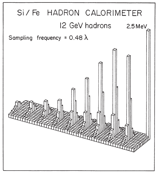
Fig. 3.28 Measured visible-energy for 12 GeV hadrons as a function of the Fe calorimeter depth
and the strip location (reprinted with permission from Borchi, E. et al., Evidence for compensation
in a Si hadron calorimeter, IEEE Transactions on Nuclear Science, Volume 40 Issue 4, Part 1-2,
Aug. 1993, pages 508–515, doi: 10.1109/23.256610,
c
° 1993 IEEE, e.g., for the list of the authors
see [SICAPO Collab. (1993a)]; see also [Leroy and Rancoita (2000)]). The depleted width of the
combined silicon detectors is ≈ 800 µm. Each strip is, on average, 40 cm long and 4 cm wide. The
total Fe depth is Fe 72 cm and the lateral coverage is 48 cm.
January 9, 2009 10:21 World Scientific Book - 9.75in x 6.5in ws-bo ok975x65˙n˙2nd˙Ed
282 Principles of Radiation Interaction in Matter and Detection
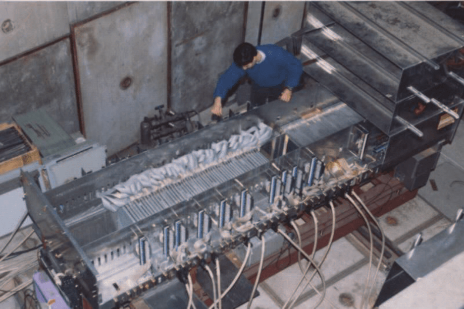
Fig. 3.29 The SICAPO calorimeter using silicon detectors (see Fig. 3.30) as active readout sampler at the PS experimental Hall at CERN.
January 9, 2009 10:21 World Scientific Book - 9.75in x 6.5in ws-bo ok975x65˙n˙2nd˙Ed
Nuclear Interactions in Matter 283
Data for a larger (≈ 99%) longitudinal containment of hadronic shower cascades are
shown in [Bitinger (1990); PDB (1996 and 1998)] and are based on experimental
data and shower parametrizations ([Bitinger (1990); PDB (1996 and 1998)] and
references therein; see also, e.g., [Bo ck et al. (1981); Hughes (1986)]).
Normally, after the primary interaction, decays of hadronic resonances created
during the energy degradation of the incident hadrons and charge-exchange re-
actions produce π
0
’s (mainly) and η’s, which will propagate electromagnetically
without any further nuclear interactions and, consequently, deposit their energy
in the form of electromagnetic cascades [Catanesi et al. (1987)]. As a result,
any hadronic cascade has purely hadronic and purely electromagnetic components
(Sect. 3.3.1). The size of this electromagnetic comp onent is largely determined by
the production of π
0
’s (and η’s) in the first interaction. After the removal of the
fluctuations due to the initial location (s
0
) of the cascade, the longitudinal profile
of a hadronic cascade can be parametrized by two terms describing the electromag-
netic and hadronic components of the cascade [Holder et al. (1978); Bock et al.
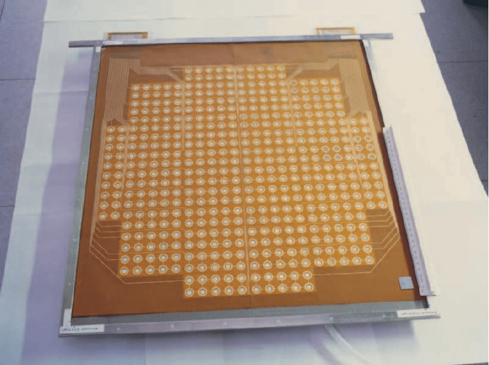
Fig. 3.30 Kapton-cover for SICAPO silicon active-sampler. The active sampler is an assembled
mosaic and consists of 2 × 2 cm
2
silicon detectors, like the one shown at the bottom right-part of
the picture.
January 9, 2009 10:21 World Scientific Book - 9.75in x 6.5in ws-bo ok975x65˙n˙2nd˙Ed
284 Principles of Radiation Interaction in Matter and Detection
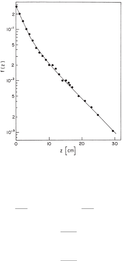
Fig. 3.31 Mean differential lateral profile f(z) as a function of the lateral distance z in cm for
incoming antiprotons of 25 GeV (adapted from Nucl. Instr. and Meth. 174, Davidov, V.A. et
al., A hodoscope calorimeter for high energy hadrons: IHEP-IISN-LAPP collaboration, 369–377,
Copyright (1980), with permission from Elsevier, e.g., for the list of the authors see [Davidov et
al. (1980)]; see also [Leroy and Rancoita (2000)]).
(1981); Della Negra (1981)]:
dE = E
½
f
em
·
x
α
e
−1
Γ(α
e
)
¸
exp(−x) dx +(1−f
em
)
·
y
α
h
−1
Γ(α
h
)
¸
exp(−y) dy
¾
, (3.79)
where E is the incident energy,
x ≡ β
e
(s − s
0
)
X
0
is the number of radiation lengths accumulated since the start at s
0
of the cascade
multiplied by a dimensionless coefficient β
e
, and
y ≡ β
h
(s − s
0
)
λ
A

January 9, 2009 10:21 World Scientific Book - 9.75in x 6.5in ws-bo ok975x65˙n˙2nd˙Ed
Nuclear Interactions in Matter 285
is the number of interaction lengths accumulated since the start at s
0
of the ca-
scade. α
e
, β
e
, α
h
, β
h
are dimensionless coefficients containing a ln(E) dependence
and are given in [Della Negra (1981)] for hadronic showers, generated in Pb and Fe
passive absorbers. Γ(α
e
) and Γ(α
h
) are the gamma functions ensuring the normal-
ization, i.e.,
Γ(α
e
) =
Z
∞
0
x
α
e
−1
exp(−x) dx (3.80)
and
Γ(α
h
) =
Z
∞
0
y
α
h
−1
exp(−y) dy, (3.81)
in such a way that a fully contained cascade should deposit all its incident energy
E. f
em
represents the fraction of electromagnetic component of the hadronic ca-
scade. The average fraction converted into electromagnetic cascade increases with
energy (as discussed at page 276).
Results of measurements (by activation methods) of the longitudinal develop-
ment of 300 GeV π
−
cascades in uranium show a profile that is very similar to
electromagnetic cascades, however, the scale is quite different since 300 GeV π
−
ca-
scades are contained at the 95% level in 80 cm of uranium, while it only takes 10 cm
to achieve the same result for electromagnetic cascades at the same energy [Leroy,
Sirois and Wigmans (1986)]. Figure 3.27 (Fig 3.28) shows the average energy de-
posited longitudinally and laterally [SICAPO Collab. (1991b, 1993a)], i.e., the so-
called visible energy, in a sampling U (Fe) SICAPO calorimeter (shown in Fig. 3.29)
employing silicon active-samplers (Fig. 3.30), as a function of the depth for 12 GeV
incoming protons. These experimental data show that the cascade maximum is lo-
cated at a calorimeter depth of ≈ 1 λ
A
and, beyond the cascade maximum, the visi-
ble energy falls following an approximate exponential dependence on the calorimeter
depth [SICAPO Collab. (1991b, 1993a)].
The 95% radial containment (R
95%
) for hadronic cascades occurs at [Amaldi
(1981); Fabjan (1986)]:
R
95%
≈ 1λ
A
. (3.82)
The hadronic cascade has a lateral spread due to the production of secondaries
at large angles [Friend et al. (1976); Davidov et al. (1980); Muraki et al. (1984)]. Its
overall transverse dependence can be approximately described by two components:
a main component along the cascade axis which decays fast, and a large and long pe-
ripheral component composed mostly of low-energy particles (including neutrons),
which carries a relevant fraction of energy away from the cascade axis. It is conve-
nient to describe the transverse profile by the sum of two exponential terms, which
represent the central core of the cascade and its halo [Davidov et al. (1980)]:
f(z) = A
1
exp
µ
−
|z − z
o
|
b
1
+ A
2
exp
µ
−
|z − z
o
|
b
2
, (3.83)

January 9, 2009 10:21 World Scientific Book - 9.75in x 6.5in ws-bo ok975x65˙n˙2nd˙Ed
286 Principles of Radiation Interaction in Matter and Detection
where z is the transverse coordinate (in cm) and z
o
is the impact point of the
cascade. For instance, A
1
/A
2
≈ 2 (i.e., A
1
≈
2
3
and A
2
≈
1
3
), b
1
= 2.2 cm and b
2
=
7.0 cm in the case of 25 GeV antiprotons showering in a Scintillator/Fe calorimeter
(Fig. 3.31) [Davidov et al. (1980)].
The ansatz [Grindhammer et al. (1989, 1990)], used to describe the lateral energy
profile of the electromagnetic cascade [cf. Eq. (2.249)], can be applied to the case
of hadronic cascades with r and the free parameter R expressed in units of λ
A
and
when the lateral resolution of the calorimeter is of the order or larger than 0.1 λ
A
. A
goo d agreement between the model and the data is obtained in the description of
the core and halo of the cascades [Grindhammer et al. (1989, 1990)]. The model also
reproduces the dependence of the lateral profile on the cascade depth and energy.
January 9, 2009 10:21 World Scientific Book - 9.75in x 6.5in ws-bo ok975x65˙n˙2nd˙Ed
Chapter 4
Radiation Environments and Damage in
Silicon Semiconductors
Silicon is the active material of radiation detectors and the basic material of elec-
tronic devices used in the fabrication and development of electronic circuits. The
present technology evolves toward the creation of faster and less power consuming
devices of increasingly small sensitive volume and higher density circuits, achiev-
ing, now, sub-micron technology with an increase of the number of memory el-
ements. These devices are then used for applications of large to very large scale
integration (VLSI) in several fields including particle physics experiments, reactor
physics, nuclear medicine and space. Many fields of application present adverse ra-
diation environments that may affect the operation of the devices. These radiation
environments are described in Sect. 4.1. These environments are generated by i)
the operation of the high-luminosity machines for particles physics experiments, an
example is the Large Hadron Collider (LHC), ii) the cosmic rays and trapped par-
ticles of various origins in interplanetary space and/or Earth magnetosphere and
iii) the operation of nuclear reactors. Their potential threats to the devices ope-
ration, in terms of damage by displacement (radiation-induced damage), are also
described in that section. A review of the characteristics of space, high-energy and
nuclear radiation environments and of physical processes inducing damages in sili-
con semiconductor operated in radiation environments was provided by Leroy and
Rancoita (2007).
The generation and type of damage are linked to processes of energy depo-
sition. The interaction of incoming particles with matter results into two major
effects: the collision energy-loss and atomic displacement, which are treated in
the chapter on Electromagnetic Interaction of Radiation in Matter. Interactions
of incoming particles, which result in the excitation or emission of atomic elec-
trons, are referred to as energy-loss by ionization or energy-loss by collisions. The
non-ionization energy-loss (NIEL) processes are interactions in which the energy
imparted by the incoming particle results in atomic displacements or in collisions,
where the knock-on atom does not move from its lattice location and the energy is
dissipated in lattice vibrations. The energy deposition by non-ionization processes
is much lower (except for neutrons) than that by ionization. However, bulk-damage
phenomena result mostly from atomic displacement deposition-mechanisms, the so-
287
January 9, 2009 10:21 World Scientific Book - 9.75in x 6.5in ws-bo ok975x65˙n˙2nd˙Ed
288 Principles of Radiation Interaction in Matter and Detection
called displacement damage. Defects, induced by the interaction of radiation with
semiconductors, are primary point-defects, i.e., vacancies and interstitials. Clusters
of defects are generated when the incident particle, such as fast neutrons, transfers
enough energy to the recoil atoms for allowing large cascades of displacements. The
change observed in semiconductor conductivity is associated with the formation of
defect clusters. Section 4.2 gives a review of the processes of energy deposition and
related damage generation including radiation-induced defects. The effect of the
processes of energy deposition and induced damage on device parameters evolution
is reviewed, in that section, considering the dependence on the type of irradia-
tion particles, their energy and fluence of irradiation. The non-ionizing energy-loss
(NIEL) scaling hypothesis is formulated in that section.
The radiation-induced defects have a large impact on bulk properties of silicon
and can be investigated by the electrical behavior of semiconductor devices (for
instance, radiation detector, diodes and transistors) after irradiation. The degra-
dation rate of minority-carrier lifetimes can be expressed in terms of a damage
coefficient. The dependence of this coefficient on the type of substrate, dopant con-
centration, level of compensation, type, energy and fluence of the irradiating parti-
cles are discussed in Sect. 4.3. After irradiation with large fast-neutron fluences at
room temperature, centers with energy-levels near the mid-gap (near the intrinsic
Fermi level ) make a significant contribution to carrier generation and determine
i) the increase of the leakage current inside the depleted region of silicon devices
and ii) modifications to the diode structure and rectification properties. Low resis-
tivity p − n diodes may gradually change their internal structure with increasing
fast-neutron fluence. In fact, non-irradiated diodes with an ohmic (n
+
) contact can
acquire an almost p − i − n structure after irradiation. Section 4.3 reviews the ef-
fects of large radiation damages and the formation of p − i − n structure at room
temperature, as well as the dependence down to cryogenic temperatures of I − V
characteristics on the type and fluence of irradiating particles. The behavior of the
junction complex-impedance is additionally discussed down to cryogenic tempera-
tures. The Hall coefficient shows whether the charges are transported by positive
or negative carriers in extrinsic semiconductors and, except for the Hall factor or
scattering factor, is the reciprocal of the carrier density and electronic charge. The
Hall coefficient provides an indication of the type and concentration of dopants in a
sample and, when combined with the resistivity, it determines the carrier mobility
(Hall mobility). The Hall coefficient is not easily interpreted to determine the type
of majority carriers, in the case of materials partly compensated by impurities of
the opposite type. Hall coefficient and Hall mobility for various types of materials
are reviewed in Sect. 4.3 as functions of the particle fluence and the Frenkel-pairs for
irradiations with several types of particles. The case of large displacement damage
is also discussed. Finally, Section 4.3 concludes with a brief review of atomic force
microscopy (AFM) investigation in irradiated devices.
The basic knowledge, discussed in this chapter, finds applications in understand-
January 9, 2009 10:21 World Scientific Book - 9.75in x 6.5in ws-bo ok975x65˙n˙2nd˙Ed
Radiation Environments and Damage in Silicon Semiconductors 289
ing the main modifications of silicon radiation-detectors and devices after irradia-
tions. These latter are discussed in Sect. 6.8 and Chapter 7, respectively.
4.1 Radiation Environments
Nowadays, silicon devices are the main components of any electronic system based
on very large scale integrated semiconductor technologies. Similarly, since decades,
silicon detectors have become the most common semiconductor radiation detec-
tor for position and energy measurements. Devices and detectors are often em-
ployed in environments degrading their performance (e.g., see [Vavilov and Ukhin
(1977); van Lint, Flanahan, Leadon, Naber and Rogers (1980); Messenger and Ash
(1992)]). These environments for space payloads and particle experiments differ
by the complexity, combination and energy distribution of the radiation and are
treated in this section. Other radiation environments, for instance nuclear weapons
(e.g., see Chapter 4 in [Messenger and Ash (1992)] and references therein) and
nuclear reactors, are beyond the scope of the present book.
4.1.1 High-Luminosity Machines Environments for Particle
Physics Experiments
Many components of the detection systems of high-energy experiments are exp osed
to the adverse radiation environment that results from the interactions, with sur-
rounding materials, of particles produced by high rate collisions of incoming beam
with target or head-on collisions of particle beams at high luminosity. The origin of
this radiation field is well understood. It is known from the time of the CERN inter-
secting storage rings (ISR) [Johnsen (1973)], the first hadron-collider, that radiation
at collider has several sources, namely, particle production at the interaction points,
possible local beam losses and beam-gas interactions, although high vacuum condi-
tion (up to 10
−11
Torr) was achieved in the accelerator vacuum chambers. Beams
could be accelerated in the ISR up to maximum energy of 31 GeV with an initial
luminosity of about 10
28
cm
−2
s
−1
. These radiation features were also encountered
at various levels at the CERN Sp¯pS-collider and hadron accelerators operated at
Fermilab, BNL and elsewhere, until extreme conditions will be reached with the
advent of the Large Hadron Collider (LHC) at CERN. Very soon, the LHC will
allow head-on collisions of 7 TeV protons with a rate of about 10
9
s
−1
p–p inelastic
events per collision, at a (designed) peak luminosity of 1×10
34
cm
−2
s
−1
, assuming a
standard inelastic p–p cross section of 80 mb. With total beam losses not exceeding
10
7
p s
−1
and beam-gas interactions limited to about 10
2
m
−1
s
−1
, the main source
of radiation at LHC will be from particles produced in p–p collisions at the inte-
raction points [ATLAS Collab. (1994b)]. High-energy particles from an interaction
point begin to cascade when entering the material of surrounding detectors. If the
material is thick, the cascade development will continue until most of the charged