Leroy C., Rancoita P.-G. Principles Of Radiation Interaction In Matter And Detection
Подождите немного. Документ загружается.

January 9, 2009 10:21 World Scientific Book - 9.75in x 6.5in ws-bo ok975x65˙n˙2nd˙Ed
290 Principles of Radiation Interaction in Matter and Detection
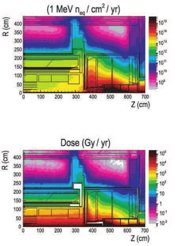
Fig. 4.1 1 MeV neutron equivalent fluence (1 MeV n
eq
/cm
2
/yr) in the ATLAS calorimetry system
and vicinity, integrated over a standard high luminosity year; Z (in cm) is the direction along the
beam axis and R (in cm) the radius around the Z-direction (from [Leroy and Rancoita (2007)]; see
also [ATLAS Collab. (1996)]).
Fig. 4.2 Yearly integrated dose (Gy/yr) for photons above 30 keV in the ATLAS calorimetry
system and vicinity for a standard high luminosity year; Z (in cm) is the direction along the
beam axis and R (in cm) the radius around the Z-direction (from [Leroy and Rancoita (2007)]; see
also [ATLAS Collab. (1996)]).
particles are absorbed. Then, one expects that charged hadrons (mainly protons,
pions) will dominate the radiation environment in regions close to the collision
point at least for small depth of traversed material (like for the LHC-ATLAS inner
detector partly equipped with silicon detectors). Particles backscattered from the
calorimeters and cascades leaking out the calorimeters produce neutrons, photons
and electrons through their interactions with surrounding material and equipment
located in the experimental hall. These particles also affect the region around the

January 9, 2009 10:21 World Scientific Book - 9.75in x 6.5in ws-bo ok975x65˙n˙2nd˙Ed
Radiation Environments and Damage in Silicon Semiconductors 291
collision point, although, neutrons in that region can be moderated by the pres-
ence of low-Z material [walls or low-Z planes of inner detectors with Z the atomic
numb er of the material (Sect. 3.1)]. While electromagnetic cascades are rapidly ab-
sorbed, neutrons will travel long distance losing their energy gradually. Therefore,
the neutron fluence dominates the radiation environment at larger radii. Nuclear
capture of thermal neutrons frequently results into production of photons. Large
amounts of photons also result from excited-state decay of spallation products and
from fast neutron interactions with atomic nuclei. Photons, produced deep inside
the material, are rapidly absorbed. Only photons, produced close to the surface of
material, have a chance to produce electrons and p ositrons and are responsible for
a low-energy electron component in the environment.
As the showering process takes a relatively long time, this mixed field of neu-
trons, photons and electrons constitutes a background with no time structure [AT-
LAS Collab. (1994b)]. The numerous scatterings of neutrons and photons before
their capture yield a uniform and isotropic field of low-energy background particles.
The radiation level induced on detector material and equipment will depend
on the position of the detector with respect to the collision point. This location is
expressed in terms of the pseudorapidity, η, defined in Eq. (3.61) and expressed as a
function of θ, which is the polar production angle with respect to the beam axis. For
experiments to be performed at LHC, the highest radiation levels are expected to oc-
cur at high pseudorapidity. As stressed above, the level of radiation also depends on
the amount of surrounding materials. In ATLAS example [ATLAS Collab. (1994b,
1996)], the forward calorimeter (FCAL) is covering the range 3.2 ≤ η ≤ 5. Due
to its location, the FCAL is subjected to radiation dose-rates up 10
6
Gy yr
−1
and
a neutron flux (neutron kinetic energy > 100 keV) up to 1 × 10
9
cm
−2
s
−1
. Repre-
senting a depth of 9.5 interaction lengths of material, the FCAL contributes to the
increase of the radiation level in the hadronic end-cap (HEC) calorimeter due to its
location (1.5 ≤ η ≤ 3.2) very close to FCAL. The HEC will be subjected to radia-
tion dose up to 0.3 kGy and a neutron fluence of 0.3 × 10
14
cm
−2
over 10 years of
operation at the highest luminosity (1 ×10
34
cm
−2
s
−1
). It is standard to use 1 MeV
equivalent neutron fluence to express neutral particle contribution to radiation. The
1 MeV equivalent neutron fluence is the fluence of 1 MeV neutrons producing the
same damage
∗
in a detector material as induced by an arbitrary fluence with a
specific energy distribution [see Eqs. (4.79, 4.85), Sects. 4.1.3 and 4.2.1]. The di-
splacement damages induced by neutrons in semiconductors can be normalized by
displacement damages induced by 1 MeV neutrons through the hardness parame-
ter [see Eqs. (4.79, 4.84), Sects. 4.1.3 and 4.2.1]. The 1 MeV neutron fluence and
yearly integrated dose (photons above 30 keV) in the ATLAS calorimetry system
∗
The amount of the induced displacement damage (i.e., the deposited damage energy, see
Sect. 4.2.1) can be defined for any kind of incident particle. However, it cannot be assumed to
relate a damage equivalence until the correlation between measured device degradation and the
calculate NIEL deposition is determined (see discussion in Sects. 4.2.1–4.2.1.5 and, also, [Griffin,
Vehar, Cooper and King (2007)]).

January 9, 2009 10:21 World Scientific Book - 9.75in x 6.5in ws-bo ok975x65˙n˙2nd˙Ed
292 Principles of Radiation Interaction in Matter and Detection
and vicinity are shown in Figs. 4.1–4.2, respectively, for a standard high luminosity
year [ATLAS Collab. (1996)]. As will be discussed later, one has also to consider
damages created by ionization processes, which are mainly inflicted to electronics
and may alter the good operation of semiconductor devices.
This part of the book addresses the study of semiconductor b ehavior in radiation
environment. However, it is interesting to look briefly at other types of detectors and
look at the impact of accelerator generated radiation field on their operation. Again,
the example of LHC will be used. Liquid argon is the active medium of FCAL,
electromagnetic and HEC calorimeters of the ATLAS experiment. The choice of
liquid argon, as active medium of these calorimeters, was largely motivated by the
radiation hardness of the technique, compared to scintillator, for instance. The
concern about activation of argon through production of
41
Ar (half-life of 1.82
hours) via the reaction
n +
40
Ar →
41
Ar + γ
↓
41
K + β
−
+ ¯ν
e
has been discarded by simulation and measurements performed at SARA [Belymam
et al. (1998)]. The short half-life of
41
Ar makes dose source negligible during access
to the detector for maintenance. Absorbers and structural materials, used in ATLAS
liquid argon calorimeters, are radiation hard and stable under irradiation. Under
irradiation, oxygen or oxygen-like impurities are released from the surface of mate-
rials and equipments immersed in liquid argon. This outgassing leads to pollution
of liquid argon and to p ossible reduction of collected ionization charge and, finally,
in turn to the reduction of the calorimeter signal. Then, the operation of the AT-
LAS liquid argon calorimeters requires limited pollution of liquid argon, below a
threshold of (1–2) ppm. This goal can be achieved if the components of the liquid
argon calorimeters are certified against release of polluting impurities under irradi-
ation. Therefore, the possible outgassing of components immersed in liquid argon
and exposed to high fluences was investigated within the ATLAS Collaboration
for several years, in conditions similar to those encountered in the running experi-
ment during LHC operation. The tested materials and equipments were subjected
to accelerated irradiation, in order to receive the equivalent of a LHC ten-year dose
within a short period of time. Cold test facilities were built at SARA [Belymam
et al. (1998)], CERI
§
and Dubna [Leroy et al. (2000a)] for that purpose. In parti-
cular, in Dubna, the large beam geometrical acceptance of 800 cm
2
at that facility
allows the exposure of relatively large area inside a one liter cryostat filled with
liquid argon. The Dubna IBR-2 pulsed neutron reactor made possible the irradia-
tion of materials and equipments immersed in liquid argon at high neutron fluences
(≈ 10
15
n cm
−2
d
−1
up to a total fluence of 10
16
n cm
−2
for a standard measurement
perio d of 11 days) and γ-doses (≈ 10 kGy per day), simultaneously, as γ’s always
§
CERI, Neutron Irradiation Facility, CNRS, Orlans, France.

January 9, 2009 10:21 World Scientific Book - 9.75in x 6.5in ws-bo ok975x65˙n˙2nd˙Ed
Radiation Environments and Damage in Silicon Semiconductors 293
accompany neutrons in the reactor. Sintered tungsten “slugs” used as absorber in
FCAL have been shown to suffer no outgassing [Leroy et al. (2000b)]. The Dubna
cold facility also allowed the test of the characteristics integrity of electronic compo-
nents under the high irradiation level expected at LHC [Leroy et al. (2002c)]. Glues
used in calorimeter electronics were selected according to their radiation hardness
and mechanical hardness under irradiation [Leroy et al. (2000c)].
The use of scintillator at LHC is mainly constrained by two factors: i) the inter-
bunch crossing time of 25 ns which requires a fast scintillator decay time and ii)
the high radiation level which requires a radiation hard scintillator. A high density
(8.28 g/cm
3
) scintillating crystal, PbWO
4
, which fulfils these constraints is used in
CMS [CMS (1997)] for electromagnetic calorimetry. Its short (long) decay time is 5
(15) ns and it is radiation hard at the expense of relatively poor light yield
†
.
Semiconductor trackers, consisting of silicon pad or pixel detectors and silicon
microstrips detectors, are used in collider experiments [ATLAS Collab. (1994b)]. Si-
licon pad detectors are also used as active medium of preshower calorimeters [AT-
LAS Collab. (1994b); CMS (1998)]. The exposure of silicon detectors or devices
to the high level of radiation encountered in high luminosity accelerators lead to
degradation of their performances. After intensive investigations, solutions have
been found to improve the condition and operation of silicon detectors in such envi-
ronment. A brief review of these solutions is presented now, more will be discussed
in subsequent chapters of this book.
Various types of damage, surface or lattice defects like vacancies (point-like
defects) or damaged regions (clusters), are produced when incoming particles de-
posit their energy in silicon. The importance of the damage created by a specific
process depends on its relative cross section compared to those of other possible
processes. One can distinguish the ionization process, resulting from the interaction
of the incident particle with the atomic electrons (e.g., see Sect. 4.2.3), and non-
ionization processes, resulting from the interaction between incoming particles and
lattice nuclei (e.g., see Sect. 4.2.1).
4.1.1.1 Ionization Processes and Collider Environments
The effect of damage to silicon devices due to ionization process originates from
ionizing energy-loss in surface layers. Even at large radii, radiations affect the elec-
tronics components located inside and around the LHC detectors through ionization
in silicon oxide by photons, protons, pions, ions (total ionizing dose - TID). The
various aspects of electronics radiation hardness have been extensively discussed
in many reports (see for instance [Dentan (1999)] in the framework of the ATLAS
experiment). The relevant TID effects for silicon devices employed in LHC environ-
ments are summarized in Sect. 4.2.3.2.
†
The light yield compared to NaI(Tl) is 0.01.
January 9, 2009 10:21 World Scientific Book - 9.75in x 6.5in ws-bo ok975x65˙n˙2nd˙Ed
294 Principles of Radiation Interaction in Matter and Detection
4.1.1.2 Non-Ionization Processes, NIEL Scaling Hypothesis and Collider
Environments
The non-ionization processes produce bulk defects or displacement damage (e.g., see
Sect. 4.2.1). The recoil nuclei are removed from their initial lattice position and
displaced into interstitial positions (interstitials). However, if the recoil energy of
the primary knock-on nucleus is higher than the threshold for atomic displace-
ment, this nucleus can produce displacement of another nucleus. Finally, as long as
the recoil energy is above displacement threshold, the cascading-process will con-
tinue and a chain of vacancies (V ) and interstitials (I) will be produced (e.g., see
Sects. 4.2.1 and 4.2.2). The bulk damage effects pro duced by energetic particles have
been shown to be proportional to the displacement damage cross-section equivalent
to the non-ionizing energy-loss [NIEL, e.g., see Sect. 4.2.1 and Eqs. (4.86, 4.88)]. The
proportionality between NIEL-value and resulting damage effects is referred to as
the NIEL scaling hypothesis. The NIEL value depends on the particle type and
energy (e.g., see Sect. 4.2.1.5). However, violations of the NIEL scaling hyp othesis
were observed. This scaling does not work for calculating N
eff
in oxygenated sili-
con [Rose Collab. (2000)] and for low proton energies for standard silicon [Bechevet,
Glaser, Houdayer, Lebel, Leroy, Moll and Roy (2002)].
Subjected to increasing fluence, the main effects on the operation of silicon de-
tectors, from a practical point of view, are i) an increase with fluence of the leakage
current, ii) an increase of the full-depletion bias voltage to be applied to the de-
tector and iii) a decrease of the charge collection efficiency (CCE). The damaged
regions created by radiation dose in the silicon bulk are acting as electrically active
defects with deep levels in the forbidden-band gap in silicon. The generation of these
additional traps decreases the carrier lifetime and increase the reverse current. For
fluences of the order of 10
14
particles cm
−2
, i.e., in practice fluences corresponding
to one year of operation, in many regions of the LHC, the reverse current can reach
values in the range of several tens of microamperes per cm
2
and even more. However,
the strong temperature dependence of the reverse current allows it to be minimized
by operating the detectors at moderate low temperature (in a range from -5
◦
C to
-10
◦
C, typically). Re-arrangement between these vacancies and interstitials or their
interactions with other defects, impurities and nuclei in the bulk (like oxygen) are
responsible of long term effects, e.g., the evolution in time of electrical characteristic
of silicon detectors such as annealing and reverse annealing of leakage current and
full depletion bias voltage after irradiation. It is observed that the leakage current
anneals following irradiation by about 50 % over a period of about two weeks at
room temperature. From the measurement of the leakage currents of silicon detec-
tors made of different starting materials irradiated with neutrons, up to fluences
of 10
15
n cm
−2
, the leakage current damage parameter is independent of the initial
resistivity and impurity concentrations, once normalized to the sensitive volume
and to the 1 MeV-neutron equivalent hadron fluence. This parameter is linked to
defect clusters which are not affected by the material. The concentration of defects,

January 9, 2009 10:21 World Scientific Book - 9.75in x 6.5in ws-bo ok975x65˙n˙2nd˙Ed
Radiation Environments and Damage in Silicon Semiconductors 295
that are responsible for the leakage current, are in the order of the impurity concen-
trations and, consequently, migrating interstitials and vacancies produced by the
irradiation are responsible for the increase of the leakage current. Annealing of the
leakage current is also material independent. The period of annealing is followed
by a fast increase of the leakage current. This reverse annealing effect is largely
moderated, even suppressed, if the irradiated diode is kept at low temperature,
around -5
◦
C. Therefore, cooling of the detector to moderately low temperatures
is a necessity for the reduction of the leakage current so keeping a signal-to-noise
ratio required for physics exploitation during colliding beam periods. This cooling is
also necessary during machine and detector maintenance periods to avoid reverse-
annealing leading to the increase of the reverse leakage current and full depletion
bias voltage.
The full depletion bias voltage is the minimal bias voltage to be applied in
order to fully deplete the detector
§
. In non-irradiated diodes, the space-charge re-
sults from shallow dopants in the silicon. Irradiation brings changes in the doping
concentration (donors and/or acceptors) with a build-up of negative space-charge
in the depletion region due to creation of deep energy levels. The effective doping
concentration being proportional to the full depletion voltage, the value of the full
depletion bias voltage is affected and can reach very high and unpractical values
after several years of the detector operation in high radiation environment. This has
the possible consequence that a fraction of the detectors will have to be operated
without being fully depleted. Similarly to the reverse leakage current, an annealing
effect is observed for the effective doping concentration (N
eff
) over a period of about
two weeks after irradiation and followed by a reverse annealing, i.e., a fast increase,
particularly after several months for diodes kept at ro om temperature. The amount
and rate of reverse annealing depends on the irradiation fluence. For a typical silicon
detector 300 µm thick and 5 kΩcm resistivity irradiated up to 10
14
p cm
−2
, the full
depletion bias voltage saturates at nearly 350 V. It should be reminded that the
operating bias voltage should always be larger than the full depletion bias voltage
due to trapping effects. This necessary over-bias depends on the exposure fluence
and state of annealing.
The charge collection efficiency (CCE) is degraded down to (10–15) % of the
value measured for non-irradiated silicon detector, depending on the irradiation
fluence. However, for temperatures below 100 K, temperature range unpractical for
LHC, 50 % of the charge is recovered in detectors irradiated up to 2 × 10
15
n cm
−2
(due to the so-called Lazarus effect
‡‡
[Palmieri et al. (1998); Bell et al. (1999)]).
In the case of liquid argon, radiation hardness is improved by selection of materi-
als certified against outgassing. For scintillator, one uses a new type of crystal with
§
The silicon detectors are typically p
+
− n junctions (e.g., see Sects. 4.3.2 and 6.8).
‡‡
It was found out that, at temperatures below 130 K, largely damaged detectors, apparently,
exhibited a significant recovery of operating conditions [Palmieri et al. (1998)]. The explanation of
this phenomenon, known as the Lazarus Effect, is related to the dynamics of the induced defects
in the semiconductor bulk.

January 9, 2009 10:21 World Scientific Book - 9.75in x 6.5in ws-bo ok975x65˙n˙2nd˙Ed
296 Principles of Radiation Interaction in Matter and Detection
increased radiation hardness. The technique, called defect engineering, is applied
to improve the radiation hardness of silicon. It involves the deliberate addition
of impurities, oxygen in practice, to the silicon bulk material during the growth
process [Rose Collab. (2000)] in order to affect the formation of electrically active
defect centers which, in turn, allow control of the macroscopic parameters of silicon
devices. The oxygen concentration achieved is [O]∼(3–5) ×10
17
cm
−3
. It should be
noted that high oxygen concentration {[O]∼(4–20) ×10
17
cm
−3
} can be found in
silicon crystals grown by the Czochralski (Cz) method. Cz growth technology was
generally characterized by low resistivity (≤ 900 Ωcm) not really suited for radia-
tion detector applications. Recently, higher resistivity Cz silicon (1.2 kΩcm) suitable
for radiation detector application became available, after developments in crystal
growth technology [Savolainen et al. (2002)]. An explanation of the behavior of
oxygen enriched silicon is found by interpreting the role played by interstitial oxy-
gen, which is believed to act as a sink of vacancies. Then, divacancy-oxygen
∗
(V
2
O)
center defects are identified as main resp onsible for the radiation-induced negative
space-charge. V
2
O is produced through the reaction:
V + O
i
→ V O, (4.1)
followed by
V O + V → V
2
O. (4.2)
The addition of oxygen in the bulk material suppresses V
2
O formation. This
happens through the interaction between interstitial oxygen with vacancies. An
increase of interstitial oxygen concentration enhances the ratio of the reactions
expressed by Eq. (4.1) and Eq. (4.2), reducing formation of V
2
O.
Oxygenation makes no difference to leakage current. Introduction of high concen-
trations [at the level of ∼ (3–5)×10
17
cm
−3
] of oxygen in silicon detectors has led to
improved radiation hardness, when the detectors were exposed to charged hadrons
(protons, pions). However, almost no improvement is observed for irradiations of
oxygenated silicon materials with neutrons of a few MeV. It should be observed that
the proton measurements have been initially done with 24 GeV/c protons at CERN-
PS, while neutron measurements at high fluences have been performed at reactors
and CERN-PS for low energy neutrons [(1–2) MeV]. The absence of measurement of
high energy neutrons (≥ 20 MeV) is due to the extreme difficulty of achieving high
fluences for neutrons of these energies during short periods of time. For instance,
neutrons of 14 MeV can be produced
†
by 38 MeV proton on a Be-target with fluences
of 10
14
n cm
−2
d
−1
, comparable to those expected at LHC. However, no measure-
ment has been done with oxygenated silicon detectors at this neutron energy. Low
energy proton (≤ 10 MeV) irradiation of silicon, doped with high concentration of
oxygen, shows improved radiation hardness of these detectors already observed for
∗
A general presentation of the radiation-induced defects can be found in Sect. 4.2.2.
†
For instance at the facility at the Nuclear Physics Institute (Academy of Sciences of the Czech
Republic), CZ-25068
ˇ
Reˇz near Prague.

January 9, 2009 10:21 World Scientific Book - 9.75in x 6.5in ws-bo ok975x65˙n˙2nd˙Ed
Radiation Environments and Damage in Silicon Semiconductors 297
24 GeV/c protons [Houdayer et al. (2003)]. The question remains if observed im-
provement is energy related, i.e., depends on the value of the proton and neutron
cross sections. Based on model, simulation [Huhtinen (2002)] and data [Bechevet,
Glaser, Houdayer, Lebel, Leroy, Moll and Roy (2002)], radiation hardness improve-
ment of oxygenated silicon is expected when it is exposed to neutrons of at least
20 MeV energy.
The different behavior between protons and neutrons, at least at low particle
energy, is of no practical consequences at LHC, since the radiation field in LHC
collision areas is largely dominated by charged hadrons, where silicon detectors are
operated, neutron acting at larger radii. Therefore the use of diffusion oxygenated
standard planar or float zone (DOFZ) silicon will be beneficial. In addition, for
proton irradiation, N
eff
achieved at high fluences is independent of the oxygenated
material initial resistivity, but for neutron irradiation, the N
eff
increase at high
fluence is reduced by the use of oxygenated material of low resistivity. Therefore,
using oxygenated silicon of low resistivity [(1–2) kΩcm] would improve their radia-
tion hardness when operated in the mixed field of charged hadrons and neutrons at
LHC.
4.1.2 Space Radiation Environment
The continuous evolution of mission requirements and their electronic technologies
for payloads and spacecrafts (for example, the International Space Station
∗∗
shown
in Fig. 4.3), combined with the need to meet the space environment constraints, par-
ticularly radiation, constitute challenges for component engineers and designers. For
instance, the increased activities in space for communications, military services and
scientific research have required to take into account that the electronics, employed
for these purposes, contain advanced devices and electronic systems in VLSI (very
large scale integration) and ULSI (ultra large scale integration) technologies, which
might have radiation sensitivity.
The space radiation is not homogenously distributed in the Earth magnetosphere
and solar cavity (the so-called heliosphere) and varies with time. As a consequence,
Low- (LEOs), Mid- (MEOs), Geosynchronous/Geostationary-Earth Orbits (GEOs),
Geostationary Transfer Orbits (GTOs) and orbits for an Earth Observatory Satellite
(EOS) have different requirements for radiation hardness (see, for instance, [Barth
(1997)] and references therein). These orbits are distinguished by their degrees of
inclination and distances of p erigee and ap ogee. The interplanetary missions are
affected by the energetic particles of solar and galactic sources traveling through
the interplanetary space (Sect. 4.1.2.4), but are less exposed to radiation effects of
the trapped particles in the Earth magnetosphere (Sect. 4.1.2.5). The fluxes of these
∗∗
Thanks to NASA’s courtesy, we show an image (Fig. 4.3) at the final stage of comple-
tion. The Reference Guide to the International Space Station is available at the web site:
http://www.nasa.gov/mission pages/station/news/ISS Reference Guide.html.

January 9, 2009 10:21 World Scientific Book - 9.75in x 6.5in ws-bo ok975x65˙n˙2nd˙Ed
298 Principles of Radiation Interaction in Matter and Detection
Fig. 4.3 Computer-generated artist’s rendering (Courtesy NASA) of the International Space Station (ISS) when completed. The ISS orbits Earth
at an altitude that ranges from 370 to 460 km.

January 9, 2009 10:21 World Scientific Book - 9.75in x 6.5in ws-bo ok975x65˙n˙2nd˙Ed
Radiation Environments and Damage in Silicon Semiconductors 299
particles are modulated by the solar wind
‡‡
, whose intensity and speed depends on
the solar activity.
The presence of this complex environment has drawn attention to the important
influence of space radiation on both the computation tools for modeling the space
radiation (e.g., see [Barth (1997)], Chapter 1 in [Claeys and Simoen (2002)], [Heyn-
derickx (2002)], Chapter 2 in [Holmes-Siedle and Adams (2002)], [Miroshnichenko
(2003)]) and the response to radiation of MOS and bipolar transistors made in
VLSI BiCMOS (Bipolar Complementary Metal-Oxide Semiconductor) technolo-
gies. These devices are, indeed, the essential part of any circuit used in that en-
vironment, thus, the knowledge of irradiation effects on them is critical (e.g., see
[Baschirotto et al. (1995b, 1996); Fleetwood et al. (1994); Johnston, Swift and
Rax (1994); Baschirotto et al. (1997); Colder et al. (2001, 2002); Codegoni et al.
(2004b); Consolandi, D’Angelo, Fallica, Mangoni, Modica, Pensotti and Rancoita
(2006)] and references therein; see, also, Sects. 4.2.3.2 and Chapter on Displacement
Damage and Particle Interactions in Silicon Devices). For instance, bipolar junction
transistors (BJT) have important applications in analog or mixed-signal IC’s and
BiCMOS circuits because of their linearity and excellent matching characteristics,
for example. Many of the bipolar integrated circuits in space systems, including op-
erational amplifiers, comparators, voltage regulators, are used to accomplish analog
functions. Furthermore, MOS transistors [particularly those of the complementary
form (CMOS)] are of wide usage in high-performance and low-power electronics.
Once defined the duration and the orbit of a satellite or a pay-load inside
the heliosphere or the Earth magnetosphere, the knowledge of fast charged par-
ticle fluences and their time dependence makes possible to determine the expected
Frenkel-pairs concentration (FP ) due to the non-ionizing energy-loss processes (see
Sect. 4.2.1) and the absorbed dose mostly determined by collision energy-loss pro-
cesses (e.g., see the chapters on Electromagnetic Interaction of Radiation in Matter
and Nuclear Interactions in Matter, and [Ziegler, Biersack and Littmark (1985a);
Ziegler, J.F. and M.D. and Biersack (2008a)])
∗
. Both types of processes result from
the interactions of charged particles impinging on semiconductor devices (i.e., on
microelectronics).
This knowledge has to be complemented by investigations of possible latch up
and single event upset (e.g., see [Messenger and Ash (1997)]) for an effective imple-
mentation of any VLSI circuit, whose design can, in turn, depend on the radiation
response (e.g., see Sects. 4.2.3.2 and 7.2). Obviously, a non-radiation hard technol-
ogy cannot be employed in a radiation environment: the space qualification of VLSI
technologies with respect to TID is certainly needed for any design consideration
and may require the qualification of their basic bipolar devices with regard to space-
radiation. As an example, when bipolar integrated circuits are exposed to radiation
‡‡
For instance, the reader can see [White (1970); Encrenaz, Bibring and Blanc (1991); Alurkar
(1997); Boella, Gervasi, Potenza, Rancoita and Usoskin (1998); Boella, Gervasi, Mariani, Rancoita
and Usoskin (2001); Grieder (2001); Lang (2001); Gosling (2006); Potgieter (2008)].
∗
The reader may also see [Leroy and Rancoita (2004)].