Leroy C., Rancoita P.-G. Principles Of Radiation Interaction In Matter And Detection
Подождите немного. Документ загружается.

January 9, 2009 10:21 World Scientific Book - 9.75in x 6.5in ws-bo ok975x65˙n˙2nd˙Ed
380 Principles of Radiation Interaction in Matter and Detection
In summary (see Table 4.5), for particle energies of typical space and high-energy
physics environments, the energy deposited by ionization is about 3–4 orders of
magnitude larger than that deposited by damage-energy for charged particles and
isotopes, while they differ marginally for fast neutrons.
4.2.3.2 Ionization Damage
Total ionizing dose (TID) causes the threshold voltage to change due to charge trap-
ping in the SiO
2
gate insulator. Ionization creates electron-hole pairs in MOS gate
oxide. In semiconductor oxide layers, such as SiO
2
, electrons produced by ionization
rapidly move from the oxide layer, under the influence of the electric field created by
the bias voltage. The holes, having lower mobility, diffuse slowly near the Si–SiO
2
interface, where they will accumulate as a charged layer, modifying the operating
features of the device. The presence of these trapped holes is responsible for an elec-
trical field which induces a negative shift of the threshold voltage, modifying the
operating features of the device (NMOS and PMOS transistors). This effect is re-
duced by the recombination of some of the electrons with holes so reducing, in turn,
the amount of holes trapped in the oxide and, consequently, reducing the negative
shift of the threshold voltage. This shift is dose-rate dependent as a high dose-rate
induces a high instantaneous density of electron-hole pairs, i.e., part of the electrons
cannot leave far the oxide and recombine very fast, causing enhancement of the re-
combination rate and reduction of the shift. In case of low dose-rate, the induced
low instantaneous density of electron-hole pairs allows electrons to quickly leave the
oxide reducing the recombination effect and the shift. After some time, a fraction
of the holes will leave the oxide at the Si–SiO
2
interface and generate defects in Si
near the interface reducing the carriers mobility. These defects are traps for electrical
charges depending on the bias applied on the gate. In PMOS transistors, the nega-
tive bias applied on the gate and the positive charges trapped in the interface states
- trapped holes in gate oxide - produce an electrical field which induces a negative
shift of the threshold voltage which enhances the threshold voltage shift initially
produced by the gate oxide trapped holes. In NMOS transistors, the positive bias
applied on the gate and the negative charges trapped at the interface produce an
electrical field which induces a positive shift of the threshold voltage which depletes
the threshold voltage shift initially produced by the gate oxide trapped holes. This
effect in NMOS transistors is also rate dependent since it depends on the density of
interface states which depends, in turn, on the holes density accumulated in the gate
oxide near the Si–SiO
2
interface. In PMOS transistors, the global threshold-voltage
shift is always negative and increases with decreasing dose-rate, while in NMOS
transistors the global threshold-voltage shift depends on the ratio between oxide
charge density and interface charge density which both increase with decreasing
dose-rate. In MOS transistors, TID effects also result in varying the sub-threshold
slope (e.g., see Chapter 1 in [Ma and Dressendorfer (1989)], also [Codegoni et al.
(2004a)] and references therein). In irradiated bipolar transistors the density of

January 9, 2009 10:21 World Scientific Book - 9.75in x 6.5in ws-bo ok975x65˙n˙2nd˙Ed
Radiation Environments and Damage in Silicon Semiconductors 381
energy states, at the interface between silicon and oxide surrounding the emitter,
is high and induces a parasitic base-current from the recombination of minority
carriers (injected from the emitter into the base) with majority carriers (from the
base). The parasitic current, added to the regular base current decreases the gain of
the bipolar transistor. However, at high collector current, saturation of the interface
states by carriers from the emitter and recombination with majority carriers from
the base brings the parasitic base current to a saturation value, which becomes
negligible and therefore the gain is almost unchanged from its value before irradia-
tion. At low collector current, the absence of interface states saturation maintains
the parasitic recombination current and degrades the gain compared with its value
before irradiation. Again, TID (see page 293) induces higher interface state density
at low dose-rate compared with high dose-rate and gain degradation induced by
TID is higher at low dose-rate than at high dose-rate. The degradation of bipolar
transistor performance by TID that increases when dose-rate decreases is called
low dose-rate effect (LDRE) and becomes significant with dose-rate ∼ 50 rad s
−1
and increases continuously with dose-rate decreasing down to 1 × 10
−3
rad s
−1
or
even less. LDRE also occurs for low TID (a few krads). From the above discussion,
LDRE depends on the device architecture, the structure and thickness of the oxide
layer surrounding the emitter and on bias conditions. LDRE degrades performance
of the bipolar circuits, in particular by degrading the gain of amplifiers, of input
offset voltages and input bias currents.
The ionizing dose affects other devices, for instance the field effect transistors. A
treatment of TID effects is beyond the purpose of the present book. However
a detailed discussion of these effects can be found in literature (e.g., see [Ma
and Dressendorfer (1989)], Chapter 6 of [Messenger and Ash (1992)], Chapter 6
of [Claeys and Simoen (2002)], [Holmes-Siedle and Adams (2002)] and, also, the
chapter on Displacement Damage and Particle Interactions in Silicon Devices and
references therein). A survey of radiation damage in semiconductor devices is given
in [ECSS (2005)].
4.3 Radiation Induced Defects and Modification of Silicon Bulk
and p − n Junction Properties
Defects and clusters of defects do not behave as donors or acceptors which are
intentionally introduced into lattice sites to modify in a controlled-way the intrinsic
properties of a semiconductor
∗
.
Radiation-induced defect centers have a major impact on the electrical behavior
of semiconductor devices and can deeply affect their properties (e.g., see [Srour,
Long, Millward, Fitzwilson and Chadsey (1984); Srour and McGarrity (1988)] and
∗
Studies have been carried out to investigate the improvement of the radiation hardness by the
so-called defect-engineering (see for instance [Kozlovski and Abrosimova (2005); Msimanga and
McPherson (2006)] and references therein).
January 9, 2009 10:21 World Scientific Book - 9.75in x 6.5in ws-bo ok975x65˙n˙2nd˙Ed
382 Principles of Radiation Interaction in Matter and Detection
references therein). For instance, centers with energy-levels near the mid-gap make
a significant contribution to carrier generation. Thermal generation of electron–
hole pairs dominates over capture processes, when the free carrier concentrations
are much lower than the thermal equilibrium values, like in the depletion re-
gions (e.g., see Chapter 6 in [Grove (1967)]). These centers become the main me-
chanism for increasing the leakage current in silicon devices after irradiation. Fur-
thermore, the electron-hole recombination occurs when a free carrier of one sign can
be captured at defect centers (or recombination centers), followed by capture of a
carrier of the opposite sign. Radiation-induced recombination centers is the relevant
mechanism to decrease the minority-carrier lifetime which, in turn, is the dominant
mechanism for gain degradation in bipolar transistors (e.g., see Sect. 7.1). In ad-
dition, donors or acceptors can be compensated by deep-lying radiation-induced
centers. That results in the decrease of the concentration of majority carriers. This
process (referred to as carrier removal) causes the variation of the device properties
depending on majority carrier concentration, for example the increase of collector
resistance in bipolar transistors. Temporary trapping of carriers can typically occur
at a shallow level, with no recombination. Both majority- and minority-carriers can
be trapped (in separate levels). Moreover, a tunneling process can allow the passage
through a potential barrier by means of defect levels. For example, there may be a
defect-assisted tunneling component of the reverse current in p −n junction diodes.
4.3.1 Displacement Damage Effect on Minority Carrier Lifetime
Among the most important semiconductor material-parameters for practical appli-
cations in electronic devices, we have the (excess-) carrier lifetime, the equilibrium
majority-carrier concentration and the majority-carrier mobility (e.g. see [Schroder
(1997)]). To a first approximation
†
, the rate at which the electrical properties of
semiconductors are degraded by irradiation is often expressed in terms of a damage
coefficient. For instance, the minority carrier (recombination) lifetime, τ , is given
by
1
τ
irr
−
1
τ
≡ ∆
µ
1
τ
¶
=
Φ
i
K
τ,i
, (4.125)
where τ
irr
and τ are the lifetimes after and b efore the irradiation with a fluence Φ
i
of particles, respectively; K
τ,i
is the (recombination) lifetime damage coefficient
‡
,
which may depend on a) the type of substrate, b) the dopant concentration, c)
the level of compensation and d) the type (“i”) and energy of irradiating particles
†
The linear dependence on the particle fluence [see Eq. (4.125)] is expected as long as the steady-
state Fermi level is not significantly moved.
‡
A coefficient that is the reciprocal of that given in Eq. (4.125) is also found and used in literature
(e.g., see Section 7.2.1 of [van Lint, Flanahan, Leadon, Naber and Rogers (1980)] and references
therein).

January 9, 2009 10:21 World Scientific Book - 9.75in x 6.5in ws-bo ok975x65˙n˙2nd˙Ed
Radiation Environments and Damage in Silicon Semiconductors 383
(e.g., see Section 5 in Chapter I of Part II of [Vavilov and Ukhin (1977)], Section 3.4
of [Srour, Long, Millward, Fitzwilson and Chadsey (1984)], [Srour and McGarrity
(1988)] and references therein). The values of K
τ,i
can be usually found in liter-
ature. For instance for low-resistivity silicon, experimental results on the lifetime
damage constants are presented in [Srour, Othmer and Chiu (1975)] for 0.5, 1.0 and
2.5 MeV electrons with fluences up to ' 3 × 10
15
e/cm
2
and 10 MeV protons with
fluences up to ' 1.2 × 10
12
p/cm
2
(see also Section 3.4 of [Srour, Long, Millward,
Fitzwilson and Chadsey (1984)]). Furthermore, the damage constant K
τ,n
was ex-
tensively investigated
††
for fast-neutron fluences (typically) up to 10
11
–10
12
n/cm
2
and its values
§
are available in literature. For n- and p-type silicon, K
τ,n
is almost
independent of the silicon resistivity (below a few Ω cm). In addition, the anneal-
ing effect on the carrier lifetime was studied at room temp erature: the minority-
carrier lifetime was found to undergo both short-term and long-term annealing (see
pages 32–45 in [Srour, Long, Millward, Fitzwilson and Chadsey (1984)] and [Srour
(1973)]).
For a fast-neutron irradiation with a spectral fluence φ(E) [where E is the kinetic
energy of the neutron, see Eq. (4.77)], the ratio Φ
n
/K
τ,n
can be re-expressed to
account for the creation of recombination centers and the absorption of minority
carriers as {see Equation (5.15) of [Messenger and Ash (1992)], and also [Codegoni et
al. (2004b); Consolandi, D’Angelo, Fallica, Mangoni, Modica, Pensotti and Rancoita
(2006)]}:
Φ
n
K
τ,n
= σ
m
ν
e
n
Si
Z
E
min
σ
c,n
(E) φ(E) dE
= σ
m
ν
e
n
Si
<σ
c,n
> Φ
n
, (4.126)
where n
Si
is the number of atoms per cm
3
in the bulk silicon [Eq. (4.82)], E
min
is the minimal threshold of the neutron energy for inducing displacement damage
(see page 348), Φ
n
is the fast-neutron fluence [Eq. (4.78)], v
e
is the average speed
of minority carriers, σ
m
is the cross section for the absorption of minority carriers
by recombination centers; σ
c,n
(E) and < σ
c,n
> are the cross section of neutrons
with energy E for creation of recombination centers in silicon and its average value,
respectively. <σ
c,n
> is computed according to
<σ
c,n
>=
R
E
min
σ
c,n
(E) φ(E) dE
Φ
n
. (4.127)
The term
C
c
= n
Si
Z
E
min
σ
c,n
(E) φ(E) dE
= n
Si
<σ
c,n
> Φ
n
[cm
−3
] (4.128)
††
The reader can see, e.g., [Messenger (1967b); Srour (1973)], Section 5 in Chapter I of Part II
of [Vavilov and Ukhin (1977)], Section 5.9 of [Messenger and Ash (1992)] and references therein.
§
Below 2–3 Ω cm [Messenger (1967b)], for n-type silicon K
τ,n
is ' (1.0–1.6) × 10
5
s/cm
2
and for
p-type silicon K
τ,n
' (1.5–3.0) × 10
5
s/cm
2
.
January 9, 2009 10:21 World Scientific Book - 9.75in x 6.5in ws-bo ok975x65˙n˙2nd˙Ed
384 Principles of Radiation Interaction in Matter and Detection
is the concentration of recombination centers resulting from the displacement pro-
cesses induced by the fast-neutrons. To a first approximation (e.g., see Sects. 7.1.1
and 7.1.3), in absence of saturation effects
¶
, (mostly) for low-resistivity silicon we
can assume that the concentration of recombination centers is proportional to the
energy deposited by non-ionizing energy-loss (NIEL) processes per unit volume E
dis
(Sect. 4.2.1) and, consequently [see Eq. (4.83)], to the concentration of Frenkel-pairs
(FP ) introduced as primary point-defects. For instance, in low-resistivity silicon the
concentration of dopants is sufficiently large to keep them participating to the phe-
nomenon of complex-defect formation even at large neutron fluences, although this
process reduces the concentration of available impurities. Therefore, Eq. (4.128) can
be expressed as
E
dis
∝ C
c
= γ
dis
FP. (4.129)
For deep defects resulting from primary defects mostly created by cascading-
displacement processes, the term γ
dis
may result to be slightly
k
(if at all) dependent
on the type of incoming particles.
By means of Eqs. (4.128, 4.129), Eq. (4.126) can be rewritten as
Φ
n
K
τ,n
= σ
m
ν
e
C
c
= σ
m
ν
e
γ
dis
FP , (4.130)
where σ
m
and ν
e
are almost independent of the properties of the fast-neutron spec-
tral fluence. These latter terms, similarly to the parameter γ
dis
, are expected to
be slightly (if at all) dependent on the type of the incoming particle, when deep
defects result from primary defects mostly created by cascading-displacement pro-
cesses. Furthermore, by combining Eqs. (4.125, 4.130), (mostly) for low-resistivity
silicon we obtain
1
τ
irr
−
1
τ
=
Φ
i
K
τ,i
' λ FP, (4.131)
where
λ = σ
m
ν
e
γ
dis
is almost independent of the type and energy of the incoming particle, but depends
on i) the type of substrate, ii) (slightly) the dopant concentration and iii) the level of
compensation. Equations (4.129, 4.131) indicate that an approximate NIEL scaling
(e.g., see Sect. 4.1.1.2) is expected for the variation of the reciprocal of the minority-
carrier lifetime in low-resistivity silicon.
Finally, it has to be added that expressions similar to Eq. (4.125) have been
formulated for the generation lifetime (e.g., see Section 11.2.4 of [Lutz (2001)]),
¶
For high-resistivity silicon (see discussion in Sect. 4.3.5), it was found that there are secondary
defects whose concentrations are not linearly dependent on fluence.
k
NIEL scaling violation was observed in high-resistivity silicon (e.g., see Sect. 6.8.3).

January 9, 2009 10:21 World Scientific Book - 9.75in x 6.5in ws-bo ok975x65˙n˙2nd˙Ed
Radiation Environments and Damage in Silicon Semiconductors 385
minority-carrier diffusion length (e.g., see Section 3.2.7.2 of [Holmes-Siedle and
Adams (2002)]), majority-carrier mobility and concentration (e.g., see Section 7.2.2
of [van Lint, Flanahan, Leadon, Naber and Rogers (1980)]).
4.3.2 Carrier Generation and Leakage Current
Silicon detectors are usually one-sided
∗∗
p
+
− n junctions
‡
and are referred to as
n-type silicon detectors. In these detectors, the highly doped p
+
-region (usually with
a dopant concentration of ≈ 10
18
cm
−3
) extends over ≈ 0.5 µm at a depth of (2–
2.5) µm and is on top of a lowly doped n-substrate (with a dopant concentration of
≈ 6× 10
11
–2.4×10
12
cm
−3
), whereas on the rear-side there is a highly doped n
+
-layer
of ≈ 0.5 µm thickness also at a depth of 2–2.5 µm and with a dopant concentration
of ≈ 10
19
cm
−3
(sometimes indicated as n
++
). One of the purposes of the n
+
-region
is to allow the n-substrate to make a good external ohmic-connection
††
(e.g., see
Section 5.1 of [Sze (1985)] and Appendix B9 of [Ng (2002)]) with, for instance, the
external bias supplier. In these devices, the electrical characteristics (for example,
I − V and C − V ) are determined by those of the one-sided p
+
− n junctions.
At room temperature, when a reverse voltage
‡‡
, V
r
, smaller than the breakdown
voltage and larger than (3k
B
T )/e ≈ 78 mV
∗
is applied to a non-irradiated silicon de-
tector, the reverse current density
†
is approximated by the sum of both the diffusion
density current in the diffusion regions and the generation current in the depletion
region (see, for instance, [Sah, Noyce and Shockley (1957); Moll (1958)], Section 3.4
of [Sze (1985)], Sections 3.7–3.8 of [Messenger and Ash (1992)], Sections 9.1–9.4
of [Bar-Lev (1993)] and Chapter 8 of [Neamen (2002)]):
J
r
≈ J
s
+
e n
int
W
τ
gn
, (4.132)
where τ
gn
is the effective generation lifetime, n
int
is the intrinsic carrier concentra-
tion (e.g., see Chapter 6), W is the depletion layer width and J
s
is the so-called sa-
turation current density. It can be shown that only those generation-recombination
centers with an energy level near the intrinsic Fermi level can significantly con-
tribute to the generation rate (see for instance [Sah, Noyce and Shockley (1957)]
∗∗
The one-sided p
+
−n junctions [Wolf (1971)] are asymmetrical step-junctions in which the p-side
is much more heavily doped than the adjacent n-side.
‡
For a description of the properties of the p − n junctions, one can see, for instance, Section 6.2
of [Wolf (1971)].
††
The non-rectifying metal-(n
+
-)semiconductor contact results in an almost abrupt junction with
the built-in potential determined by the metal work-function, the electron affinity of the semicon-
ductor and the potential difference between the Fermi level and the bottom level of the conduction
band; the current transport is mainly due to majority carriers (e.g., see pages 160–171 of [Sze
(1985)]).
‡‡
In this Section, V
r
indicates the absolute value of the reverse voltage.
∗
k
B
is the Boltzmann constant, T the is temperature in Kelvin and e = 1.6 × 10
−19
C is the
electronic charge.
†
The contribution of the surface leakage current (e.g., see Section 10.3 of [Grove (1967)]) has not
been taken into account in Eq. (4.132) (see also Sects. 6.1.6).

January 9, 2009 10:21 World Scientific Book - 9.75in x 6.5in ws-bo ok975x65˙n˙2nd˙Ed
386 Principles of Radiation Interaction in Matter and Detection
and Section 3.4 of [Sze (1985)]). For an n-type silicon detector, the saturation den-
sity current is expressed by that of the real diode equation, i.e.:
J
s
≈ e
n
2
int
N
d
s
D
p
τ
p
, (4.133)
where N
d
is the donor concentration, D
p
and τ
p
are the diffusion coefficient and the
lifetime of holes in the n-region, respectively.
As mentioned above, radiation-induced defect centers, whose energy levels are
near the intrinsic Fermi level, can become a relevant source for carrier generation
and determine the increase of the volume-generated reverse-bias current inside the
depleted region of silicon devices. Since, to a first approximation, the concentration
of defects is proportional to the particle fluence, the reverse current after the irradi-
ation (I
r,irr
) is expected to increase with increasing particle fluence. Experimental
studies
∗
carried out on reverse-biased silicon detectors have confirmed that I
r,irr
(in A) depends, to a first approximation, linearly on the particle fluence:
I
r,irr
' I
r
+ α
i
V
vol
Φ
i
, (4.134)
where I
r
(in A) is the detector leakage current before the irradiation at a fluence
Φ
i
(in particles/cm
2
), V
vol
(in cm
3
) is the depleted volume of the detector and α
i
(in A/cm) is the so-called radiation-induced reverse current damage constant. This
latter coefficient depends, in turn, on the type (“i”) and energy of the irradiating
particles (see Sects. 4.2.1.1–4.2.1.5). The processes resulting in self-annealing at
room temperature (see page 373) allow the leakage current to decrease with time.
The time dependence of the leakage current was investigated from 1.5 hours up
to 26 months after the irradiations of high-resistivity
†
Fz silicon detectors exposed
to 2 MeV neutrons with fluences between 4.8 ×10
12
and 1.3 ×10
13
n/cm
2
[SICAPO
Collab. (1994b)]. The detectors were stored and kept at room temperature. The mea-
surements were performed at a temperature of 20
◦
C and at full depletion voltage. It
has been determined that the reverse current damage constant (α
n
) decreases with
time as
α
n
= 10
a
t
−b
× 10
−17
[A/cm], (4.135)
where a = 1.17 ±0.01, b = (1.45 ±0.86) ×10
−1
and t (≥ 1.5) is the numb er of hours
after the irradiation [SICAPO Collab. (1994b)]. After a long-term annealing, the
reverse current damage constants are ≈ 2 × 10
−17
[A/cm] and ≈ 3 × 10
−17
[A/cm]
for 1 MeV neutrons and minimum ionizing protons (and pions), respectively (see
Section 28.8 of [PDB (2008)] and, also, [Moscatelli et al. (2002)]).
At higher fast-neutron fluences, a stronger rise of I
r,irr
as function of the neu-
tron fluence was observed (see, for instance, Fig. 11.11 in Section 11.2.4 of [Lutz
∗
One can see, for instance, Sect. 6.8.2 and, also, [Fretwurst et al. (1993); Leroy, Glaser, Heijne,
Jarron, Lemeilleur, Rioux, Soave and Trigger (1993); SICAPO Collab. (1994b)], [Bechevet, Glaser,
Houdayer, Lebel, Leroy, Moll and Roy (2002)], Section 6.4.1 of [Holmes-Siedle and Adams (2002)]
and references therein.
†
The resistivities were between (4–7) kΩ cm.

January 9, 2009 10:21 World Scientific Book - 9.75in x 6.5in ws-bo ok975x65˙n˙2nd˙Ed
Radiation Environments and Damage in Silicon Semiconductors 387
(2001)]). In fact, at these fluences, the I − V reverse characteristics are largely
modified (e.g., see Sect. 4.3.3.1) and determine an increase of the effective reverse
current damage constant.
4.3.3 Diode Structure and Rectification Down to Cryogenic
Temperature
The characteristics of semiconductor diodes, like those of other semiconductor de-
vices, are substantially affected by irradiation. The rate and level of radiation
changes involve the properties of the bulk region, of the ohmic contact and the
surface effects. Thus, at large fluences, both the forward and reverse I − V cha-
racteristics are different with respect to those of a non-irradiated diode. After ir-
radiation, these characteristics depend on the type and fluence of particles and on
the junction and bulk properties of the silicon. For instance, at large particle flu-
ences, semiconductor diodes lose (largely) the features of being a rectifying device
to become more similar to linear semiconductor resistors with a low (germanium) or
high (silicon) resistivity (see for instance Section 1 in Chapter II of Part I I of [Vav-
ilov and Ukhin (1977)], [Croitoru, Gambirasio, Rancoita and Seidman (1996)] and
references therein).
4.3.3.1 Rectification Property Up to Large Fast-Neutron Fluences at Room
Temperature
The rectification property of a p − n diode results from the creation of a depletion
region at thermal equilibrium. It is one of the most important characteristics of
non-irradiated p − n junctions, that is they allow current to flow easily in one
direction. When we apply a forward bias, the electrostatic potential across the
junction region is reduced from that of the thermal equilibrium [the so-called built-in
potential, see Eq. (6.12)], thus the diffusion of majority carriers from one to the other
side of the junction is enhanced and, as a consequence, the forward current increases
rapidly with increasing voltage. However, under reverse bias, the applied voltage
increases the electrostatic potential across the depleted region, as a consequence
determines a decrease of the diffusion currents and, finally, results in a small reverse
(or leakage) current. As the reverse bias is increased, the reverse current remains
very small [Eq. (4.132)], until a critical voltage (the so-called breakdown voltage) is
reached. Above the breakdown voltage, the reverse current becomes very large
‡
.
The forward current-voltage characteristics of a non-irradiated diode accounts
for both the diffusion and recombination currents (see for instance [Sah, Noyce
and Shockley (1957); Moll (1958)], Section 3.4 of [Sze (1985)], Sections 3.7–3.8
of [Messenger and Ash (1992)], Sections 9.1–9.4 of [Bar-Lev (1993)] and Chapter 8
of [Neamen (2002)]). In fact under low-injection condition
§
and assuming that the
‡
This phenomenon is also referred to as junction breakdown.
§
This condition is satisfied when the injected minority carrier concentrations are small compared
January 9, 2009 10:21 World Scientific Book - 9.75in x 6.5in ws-bo ok975x65˙n˙2nd˙Ed
388 Principles of Radiation Interaction in Matter and Detection
depletion region of the diode has abrupt boundaries, the ideal diode equation for
the density current due to carrier diffusion (J
f,diff
) is replaced by the real diode
equation:
J
f
' J
f,diff
+
e n
int
W
2τ
rc
exp
µ
e V
f
2 k
B
T
¶
, (4.136)
where V
f
is the applied forward voltage
¶
, τ
rc
is the effective recombination lifetime,
n
int
is the intrinsic carrier concentration, W is the depletion layer width and J
f,diff
is given by
J
f,diff
= J
s
·
exp
µ
e V
f
k
B
T
¶
− 1
¸
. (4.137)
J
s
is the saturation current density and is given by Eq. (4.133) for n-type silicon
detectors. The second term of Eq. (4.136) accounts for the so-called generation
current in the depletion layer width. It can be shown that only those generation-
recombination centers with an energy level near the intrinsic Fermi level can con-
tribute significantly to the recombination rate (see for instance [Sah, Noyce and
Shockley (1957)] and Section 3.4 of [Sze (1985)]).
In general, the measured forward currents can be represented empirically by:
I
f
∝ exp
µ
e V
f
η k
B
T
¶
, (4.138)
where η is referred to as ideality factor
k
. At ro om temperature, in silicon p − n
diodes the recombination current dominates at low-forward voltages, while for V
f
>
0.5 V the diffusion current dominates (e.g., see Fig. 6.24 in Section 6.6.b of [Grove
(1967)]). At even larger forward currents, the ideality factor becomes again larger
than 1. This phenomenon results from the effect of series resistance and from the
high-injection of carriers.
In p − i − n diodes, there is an almost-intrinsic (or a weakly doped) layer sand-
wiched between the heavily doped p
+
- and n
+
-regions
∗∗
. In practice, the central
region is either weakly doped p-type (indicated as π-) or weakly doped n-type (in-
dicated as ν-) silicon, with typical dopant concentrations of ≈ (10
12
–10
13
) cm
−3
and ranges ≈ (10–200) µm (see, for instance, Chapter 2 of [Ng (2002)]). In these
diodes, the I −V characteristic is approximately expressed by (e.g., see Section 15.2d
of [van der Ziel (1976)], Sections 3.1–3.3.1.1 of [Ghandhi (1977)], Section 11.2
of [Tyagi (1991)], Chapter 2 of [Ng (2002)], see also [Fletcher (1957); Nussbaum
(1973)]):
I
f,pin
∝ F
L
exp
µ
e V
f
m k
B
T
¶
, (4.139)
with the majority carrier concentrations.
¶
In this Section V
f
indicates the absolute value of the applied forward voltage.
k
The ideality factor is ' 1 when the diffusion current dominates, ' 2 when the recombination
current dominates.
∗∗
The size of the n
+
-region (see for instance the doping profiles of a silicon p
+
− n − n
+
power
rectifier in Section 18.1.1 of [Tyagi (1991)] and references therein) is such that it does not operate
only as an ohmic contact, as it occurs in p
+
− n junction.
January 9, 2009 10:21 World Scientific Book - 9.75in x 6.5in ws-bo ok975x65˙n˙2nd˙Ed
Radiation Environments and Damage in Silicon Semiconductors 389
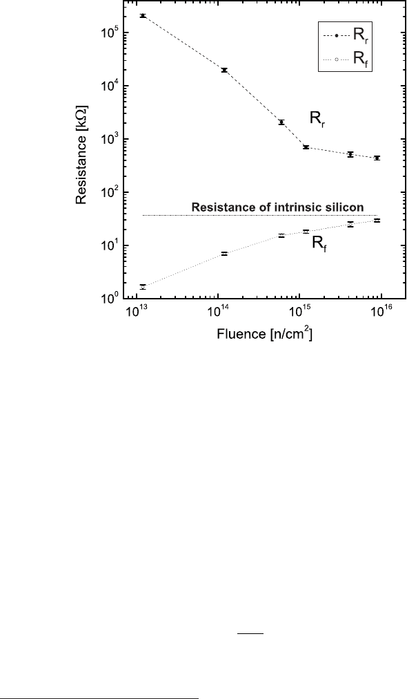
Fig. 4.25 Reverse (R
r
) and forward (R
f
) resistances in kΩ as functions of the fast neutron fluence
in n/cm
2
at room temperature (from [Leroy and Rancoita (2007)]; see also [Croitoru, Gambirasio,
Rancoita and Seidman (1996)]). The dotted and dashed lines are to guide the eye. For these
detectors the equivalent resistance, in case of an intrinsic silicon medium, was calculated for an
intrinsic silicon resistivity of about 2.3 × 10
5
Ω cm at 300 K (see, for instance, Table 1.20 of [Wolf
(1971)]).
where 1 < m < 2 depends on the dopant concentrations and on the levels of
the recombination centers [Nussbaum (1973)]. F
L
is a function of the ratio w/L
a
,
where w is the thickness of the quasi-intrinsic layer and L
a
is the ambipolar diffusion
length: it reaches its maximum value (≈ 0.3) for w/L
a
≈ 1 (e.g., see Sections 3.1–
3.3.1 of [Ghandhi (1977)]).
At room temperature, the forward (and reverse) I − V characteristics of n-
type silicon detectors
††
of 400 µm thickness and resistivity (4–6) kΩ cm have been
measured before and after irradiation with fast-neutrons. Before irradiation, for
3.8 .
e V
k
B
T
. 25
these low-doped devices exhibit an ideality factor which is larger than that expected
from Eq. (4.138) and becomes ≈ 4 at large V
f
[SICAPO Collab. (1995d)]
∗
. After
††
The dopant concentrations of the layers are close to those indicated at page 385.
∗
The ideality factor was also found to be larger than expected in 300 µm thick devices [Beattie,
Chilingarov and Sloan (1998)].