Leroy C., Rancoita P.-G. Principles Of Radiation Interaction In Matter And Detection
Подождите немного. Документ загружается.

January 9, 2009 10:21 World Scientific Book - 9.75in x 6.5in ws-bo ok975x65˙n˙2nd˙Ed
390 Principles of Radiation Interaction in Matter and Detection
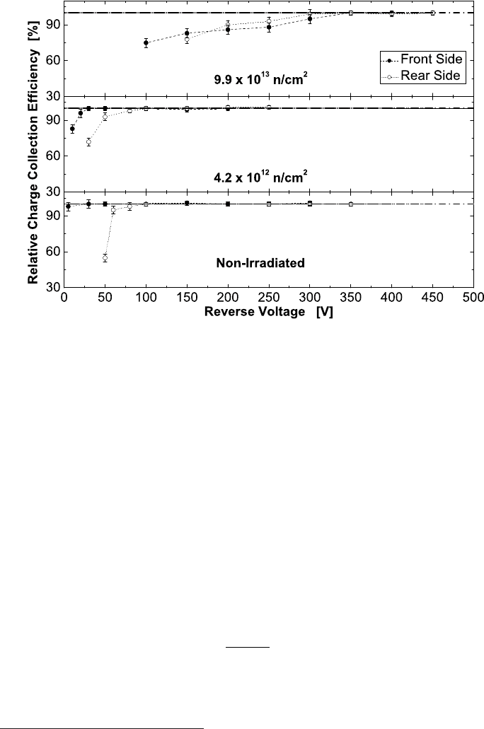
Fig. 4.26 Relative charge-collection efficiency (R
eff
, see text at page 393) measured with an
241
Am α-source located at the front (•) and at the rear (◦) of non-irradiated and irradiated silicon
detectors with fast-neutron fluences of 4.2 × 10
12
n/cm
2
and 9.9 × 10
13
n/cm
2
(from [Leroy and
Rancoita (2007)]; see also [SICAPO Collab. (1994b,c)]). The dashed line and dotted line are to
guide the eye. The dashed and dotted line represents R
eff
= 100%.
irradiation
†
, the forward I −V characteristic is modified and becomes a function of
the fast-neutron fluence [SICAPO Collab. (1995d)]: a similar behavior was experi-
mentally observed in other silicon detectors and photodiodes {e.g., see, for silicon de-
tectors, [Croitoru, Gambirasio, Rancoita and Seidman (1996); Beattie, Chilingarov
and Sloan (1998, 2000); Granata et al. (2000)] and, for high-resistivity (≈ 5 kΩ cm)
n-type photodiodes, [Korde et al. (1989)]}. In addition [see Eq. (4.138)], at the
fluence of ≈ 10
14
n/cm
2
I
f,irr
depends exponentially on V
f
(with an ideality factor
of ≈ 2 [SICAPO Collab. (1995d)]) only up to ≈ 0.13 V (i.e., (e V )/(k
B
T ) ≈ 5). In
practice, for fluences & 1.2 × 10
13
n/cm
2
, the experimental data show that I
f,irr
depends linearly on V
f
[Croitoru, Gambirasio, Rancoita and Seidman (1996)] above
a critical forward voltage V
f,c
which depends, in turn, on the fluence, i.e.,
I
f,irr
= C
f
(Φ
n
) +
V
f
R
f
(Φ
n
)
, for V
f
> V
f,c
(Φ
n
). (4.140)
V
f,c
(Φ
n
) varies from ≈ 1.2 V at the fluence of 1.2 × 10
13
n/cm
2
up to ≈ 8 V at
8.9 × 10
15
n/cm
2
. At the critical voltage
‡
V
f,c
, I
f,irr
is 300–350 µA. The absolute
values of C
f
(Φ
n
)
§
are small but not negligible compared with I
f,irr
(V
f,c
). Thus,
†
Experimental data are available up to fast-neutron fluences of ≈ 10
16
n/cm
2
.
‡
Before irradiation, for I
f
≈ 350 µA we have V
f
. 0.5 V.
§
C
f
(Φ
n
) is negative for fast-neutron fluences up to ≈ 1.2 × 10
14
n/cm
2
and positive at larger

January 9, 2009 10:21 World Scientific Book - 9.75in x 6.5in ws-bo ok975x65˙n˙2nd˙Ed
Radiation Environments and Damage in Silicon Semiconductors 391
Table 4.6 Values of the parameters m
eff
and b
eff
in
Eq. (4.143) for Fz-detectors with resistivities ranging from
5 to 7 kΩ cm [SICAPO Collab. (1994b)]. These parameters
have been computed for an α source located at the front
and at the rear side of silicon detectors (from [Leroy and
Rancoita (2007)]).
Front Side Rear Side
m
eff
(×10
−2
) -5.12 ±0.93 -7.51 ±0.88
b
eff
1.64 ±0.13 1.94 ±0.12
Eq. (4.140) expresses that the device behaves nearly as an ohmic medium, al-
though a (largely) reduced rectification is maintained even at the largest fluence
([Croitoru, Gambirasio, Rancoita and Seidman (1996)], see also [SICAPO Collab.
(1995d); Beattie, Chilingarov and Sloan (1998, 2000); Granata et al. (2000)]). In
Fig. 4.25, the values of the forward resistance (R
f
) are shown as a function of the
fast-neutron fluence: they approach that of the intrinsic silicon with increasing
fluence.
In these detectors irradiated with fast neutron fluences & 1.2 × 10
13
n/cm
2
,
the reverse I − V characteristics show that the reverse current I
r,irr
monotonously
increases with V
r
([Croitoru, Gambirasio, Rancoita and Seidman (1996)], see also
[Granata et al. (2000)]), i.e., the current does not approach a constant value as
predicted by Eq. (4.132). At large reverse bias, I
r,irr
becomes linearly dependent on
V
r
:
I
r,irr
= C
r
(Φ
n
) +
V
r
R
r
(Φ
n
)
, for V
r
> V
r,c
(Φ
n
), (4.141)
where V
r,c
(Φ
n
) is ≈ 350 V at fluences between 1.2 ×10
13
and 6 ×10
14
n/cm
2
and ≈
90 V at 8.9×10
15
n/cm
2
. At the critical voltage V
r,c
, I
r,irr
is ≈ 5.5 µA (≈ 300 µA) at
1.2×10
13
n/cm
2
(8.9×10
15
n/cm
2
). In Fig. 4.25, the values of the reverse resistance
(R
r
) are shown as a function of the fast-neutron fluence: similarly to those of
the forward resistance, they approach that of the intrinsic silicon with increasing
fluence. The rectification ratio, defined as
R
r/f
(Φ
n
) =
R
r
(Φ
n
)
R
f
(Φ
n
)
, (4.142)
is ≈ 1.27×10
5
at 1.2×10
13
n/cm
2
and decreases down to ≈ 14.8 at 8.9×10
15
n/cm
2
.
In silicon rectifying diodes
‡‡
, similarly to low-doped detectors, an increase of the
fast-neutron fluence causes a decrease of the forward I − V characteristic. At large
fluences [Croitoru, Gambirasio, Rancoita and Seidman (1996)].
‡‡
One can see, e.g., [Easley (1962); Frank, Poblenz and Howard (1963)], Section 1 in Chapter II of
Part II of [Vavilov and Ukhin (1977)] and also Sections 6.5 and 6.8.1 of [Holmes-Siedle and Adams
(2002)].

January 9, 2009 10:21 World Scientific Book - 9.75in x 6.5in ws-bo ok975x65˙n˙2nd˙Ed
392 Principles of Radiation Interaction in Matter and Detection
fluences, the I − V characteristic for both p − n and p − i − n rectifying diodes is
approximately expressed by Eq. (4.140), where C
f
(Φ
n
), R
f
(Φ
n
) and V
f,c
(Φ
n
) depend
on the dopant concentrations. In addition, in p − n diodes V
f
(Φ
n
) increases with
increasing base thickness; in p−i−n diodes it increases with increasing the thickness
of the quasi-intrinsic i-layer (Figs. 82–85 at pages 204–207 of [Vavilov and Ukhin
(1977)], see also [Shwartz et al. (1966)]). The experimental data on silicon p−n and
p − i − n irradiated diodes show a qualitative and quantitative agreement with the
predictions based on the Vavilov–Ukhin model (see pages 188–208 of [Vavilov and
Ukhin (1977)]).
4.3.3.2 Large Radiation Damage and p −i −n Structure at Room Tempe-
rature
It has been observed that p − n diodes, with resistivities of several Ω cm, may
gradually change their internal structure with increasing fast-neutron fluence. In
fact, non-irradiated diodes with an ohmic (n
+
-) contact can acquire a p − i − n
structure after irradiation. This was determined, for instance, by measurements
of the potential distribution with respect to the p-region using the method of a
moving probe. These measurements show that, in a forward-biased device with a
resistivity of ≈ 32 Ω cm, an increased voltage drop occurs in the base-region and in
the ohmic-contact with increasing neutron fluence above ≈ 2 ×10
13
n/cm
2
(e.g., see
Fig. 86 at page 208 of [Vavilov and Ukhin (1977)]). The n
+
− n ohmic-contact
properties are conserved in lower resistivities devices (≈ 2.1 Ω cm) up to fluence of
≈ 2 × 10
14
n/cm
2
.
Similarly to low-resistivity p − n diodes, n-type detectors with an n
+
-region as
ohmic-contact (e.g., see Sect. 4.3.3.1) gradually change their internal structure. In
fact, with increasing particle fluence, the n-doped region becomes almost intrinsic
(i, i.e., very weakly doped) and the n
+
-layer behaves like a rectifying region. In addi-
tion, at fast-neutron fluences of ≈ 10
14
n/cm
2
, the behavior of the p
+
−n device has
been found to be compatible with that of a p
+
−i−n
+
diode with an ambipolar dif-
fusion length (e.g., see page 389) of ≈ 200 µm [SICAPO Collab. (1995d)]. This phe-
nomenon has been confirmed [SICAPO Collab. (1994b,c)] by employing fast shaped
electronics [i.e., shaped signals of (20–25) ns peaking-time and ≈ 120 ns base-time]
for measuring the charge collection
¶
, when an
241
Am α-source is located at the front
or at the rear of non-irradiated and irradiated silicon detectors
k
. The total range
of an α-particle from an
241
Am source is about 25 µm in silicon. As a consequence,
the depleted layer width must be ≥ 25 µm in order to obtain the maximum (or full)
charge-collection. Before irradiation (see Fig.4.26), full charge-collection is achieved
at low reverse bias (a few volts), when the source is located at the front of the de-
¶
A treatment of the charge transport and collection in silicon diodes can be found in the chapter on
Solid State Detectors (see also Sects. 6.1.4, 6.1.5 and 6.8.2).
k
These devices are Fz-silicon detectors (400 µm thick) with resistivities ranging from 5 to 7 kΩ cm
[SICAPO Collab. (1994b)].

January 9, 2009 10:21 World Scientific Book - 9.75in x 6.5in ws-bo ok975x65˙n˙2nd˙Ed
Radiation Environments and Damage in Silicon Semiconductors 393
tector (i.e., of the p
+
-region), while the reverse voltage for full depletion (≈ 100 V)
is needed to achieve a full charge-collection when the source is located at the rear
side of the detector (i.e., of the n
+
-layer for the ohmic-contact). Furthermore, the
reverse voltage for maximum charge-collection increases with increasing fluence
∗∗
(e.g., see Fig. 4.26 for 4.2 × 10
12
n/cm
2
and 9.9 × 10
13
n/cm
2
). At the fluence of
9.9 × 10
13
n/cm
2
(Fig. 4.26), the maximum charge-collection is obtained for an ap-
plied reverse voltage of ≈ 350 V. As expected
∗
, the applied voltage exceeds largely
that needed for full charge-collection before irradiation. In addition, the front and
rear sides of the detector seem to b ehave similarly, i.e., the device operates as a
double-sided junction and not as an asymmetrical (one-sided) junction [SICAPO
Collab. (1994b)]. In these high resistivity silicon detectors, the charge-collection
efficiency (e.g., see Sect. 6.8.2), i.e., the ratio R
eff
of the charge collected after irra-
diation with respect to that of before irradiation, was found to have a logarithmic
dependence on fluence. The charge collected is roughly that before irradiation up
to a fluence of ≈ 3.2 × 10
12
n/cm
2
[SICAPO Collab. (1994b)]. Above this fluence,
R
eff
decreases and is given by
R
eff
∼ m
eff
ln (Φ
n
) + b
eff
, for Φ
n
> 3.2 × 10
12
n/cm
2
, (4.143)
where Φ
n
is the fast-neutron fluence, and the coefficients m
eff
and b
eff
, for
Fz-detectors with resistivities ranging from 5 to 7 kΩ cm, are shown in Ta-
ble 4.6 [SICAPO Collab. (1994b)]. R
eff
slightly depends on the location of the
α-source, i.e., at the front or at the rear side of the silicon detector
††
. In Fig. 4.26,
the relative charge-collection efficiency (as a function of the applied reverse voltage)
is the fraction (in percentage) of the charge collected with respect to the maximum
charge collected after irradiation whose R
eff
is expressed by means of Eq. (4.143).
After irradiations in the range (1–10)×10
14
n/cm
2
, high-resistivity silicon detec-
tors are still capable of measuring the energy-loss deposited by minimum-ionizing-
particles (mips) under both reverse and forward bias [Chilingarov and Sloan (1997);
Beattie, Chilingarov and Sloan (2000)]. To reduce the leakage current, these detec-
tors were operated at moderate low-temperature up to about 249 K.
4.3.3.3 I − V Characteristics Down to Cryogenic Temperature
The carrier concentration of an extrinsic non-irradiated silicon semiconductor re-
mains essentially constant over a wide range of temperature below 300 K. However,
at low temperature the dopant atoms are no longer fully ionized
‡‡
and the electron
(hole) concentration depends on the concentration of acceptors (donors) contained
in n-type (p-type) silicon. In fact, sophisticated purification techniques can largely
∗∗
The depletion voltage for full charge-collection decreases with decreasing temperature
(e.g, see [Granata et al. (2000); Santocchia et al. (2004)]).
∗
One can see, e.g., [Rancoita and Seidman (1982); Borgeaud, McEwen, Rancoita and Seidman
(1983); SICAPO Collab. (1994b,c)], see also Section 11.2.4 [Lutz (2001)].
††
Similar results were also obtained with MCZ detectors [SICAPO Collab. (1994c)].
‡‡
This temperature range is also referred to as freeze-out range of temperature.

January 9, 2009 10:21 World Scientific Book - 9.75in x 6.5in ws-bo ok975x65˙n˙2nd˙Ed
394 Principles of Radiation Interaction in Matter and Detection
reduce “unwelcome” impurities, but not eradicate them completely. In addition with
decreasing temperature, while the energy gap (E
g
) slightly increases, the Fermi level
(E
F
) approaches the energy level of the main impurity.
For instance, in an n-type extrinsic semiconductor, the electron concentration
(n
0
) at low (and very low) temperature
∗∗
is given by:
n
0
=
p
g
d
N
c
N
d
exp
µ
E
d
− E
c
2 k
B
T
¶
, for N
a
¿ n
0
¿ N
d
, (4.144)
and
n
0
= g
d
N
c
·
N
d
− N
a
N
a
¸
exp
µ
E
d
− E
c
k
B
T
¶
, for n
0
¿ N
a
< N
d
, (4.145)
where N
d
and N
a
are the concentrations of donor and acceptors, respectively, with
N
d
> N
a
, E
d
and E
c
are the energy level of the principal donor and the energy
of the bottom of the conduction band
∗
, respectively; N
c
is the effective density-
of-states in the conduction band
†
and g
−1
d
(= 2) is the ground-state degeneracy
‡
of the simple donor (e.g., Section 1.4.3 of [Sze (1981)] and Section 3.1.1 of [Blake-
more (1987)]). The expressions regarding the hole concentration in a p-type extrin-
sic semiconductor at low temperature can be found, for instance, in Section 3.2.2
of [Blakemore (1987)]. It has to be noted that the intrinsic-carrier concentration
(n
int
) also decreases with decreasing temperature. n
int
is approximately given by
(e.g., Section 3.4.1 of [Wolf (1969)])
n
int
≈ 3.73 × 10
16
× T
3/2
exp
µ
−
7.014
T
× 10
3
¶
cm
−3
, (4.146)
becomes ∼ 10
8
cm
−3
at T ∼ 250 K (e.g., see Fig. 3.4.1 at page 179 of [Wolf (1969)],
Fig. 11 at page 19 of [Sze (1981)]) and very small at T ≈ (150–170) K. Other
expressions and comparisons with experimental data can be found in [Barber (1967)]
(see also Sections 1.2.1.3 and 1.2.2.3 of [Guti´errez, Deen and Claeys (2001)]).
Furthermore {e.g. see Equation (322.11) at page 137 of [Blakemore (1987)]} at
very low temperature, the energy of the Fermi level is given by:
E
F
∼ E
d
+ k
B
T ln
·
g
d
(N
d
− N
a
)
N
a
¸
for n
0
¿ N
a
< N
d
. (4.147)
By inspection of Eq. (4.147), we see that the Fermi level moves to that of the prin-
ciple donor as T → 0 K. While, as T increases from absolute zero, it (slightly)
∗∗
The reader can see, e.g., Equations (322.7, 322.8) in Section 3.2.2 of [Blakemore (1987)] and,
also, Section 1.4.3 of [Sze (1981)].
∗
E
c
− E
d
is (0.044–0.045) eV for phosphorus at room temperature in silicon (e.g., see Chapter 1
of [Milnes (1973)]).
†
In silicon {e.g., see page 19 of [Sze (1985)] and Equation (220.1) at page 82 of [Blakemore
(1987)]}, N
c
is 4.829 × 10
15
[m
n
(T )/m
e
]
3/2
T
3/2
cm
−3
, where m
e
is the electron rest mass
and m
n
(T ) is the density-of-states effective mass for electrons ≈ 1.18 (1.06) at 300 (4.2) K
(e.g., see [Barber (1967)] and Section 1.2.1.3 of [Guti´errez, Deen and Claeys (2001)]; additional
data can be found in Section 2.7 of [Adachi (2004)]).
‡
For acceptors, the degeneracy factor is 4 {e.g., see Equation (151.1) at page 58 and Equa-
tion (220.1) at page 82 of [Blakemore (1987)] and, also, page 19 of [Sze (1985)]}.
January 9, 2009 10:21 World Scientific Book - 9.75in x 6.5in ws-bo ok975x65˙n˙2nd˙Ed
Radiation Environments and Damage in Silicon Semiconductors 395
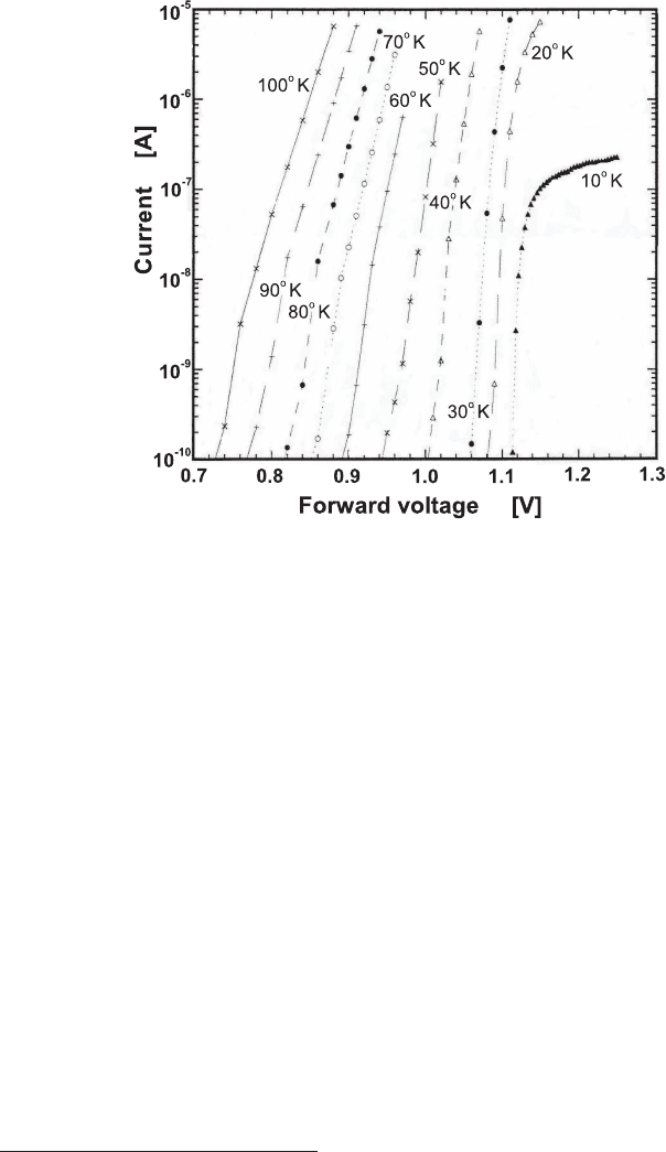
Fig. 4.27 Forward current (in A) as a function of the applied forward voltage (in V) for a non-
irradiated n-type silicon detector and temperatures from 10 up to 100 K (from [Leroy and Rancoita
(2007)]; see also [Croitoru, Rancoita, Rattaggi, Rossi and Seidman (1996, 1997)]).
rises above E
d
in extrinsic semiconductors with a small compensation [i.e. for
g
d
(N
d
− N
a
) > N
a
], before decreasing again at larger temperatures. At 10 K for
an acceptor compensation of about 1 %, E
F
− E
d
is ≈ (2–4) meV {Eq. (4.147), see
also Fig. 32.10 at page 137 of [Blakemore (1987)]}.
As mentioned above, the energy gap depends on the temperature: for a weakly
doped Fz-material with N
a
= 5 × 10
12
cm
−3
and N
d
= 10
12
cm
−3
[Bludau and
Onton (1974)], it is about 1.12 eV at 300 K and about 1.17 eV at (50–10) K (see
also Section 1.2.1.2 of [Guti´errez, Deen and Claeys (2001)] and, for instance, direct
measurements reported in [MacFarlane, McLean, Quarrington and Roberts (1958);
Shklee and Nahory (1970); Bludau and Onton (1974)]).
In Fz n-type detectors
§
with resistivity of ≈ (4–7) kΩ cm (i.e., a dopant concen-
tration of ≈ 1.1×10
12
–6.2×10
11
cm
−3
), the acceptor concentration is typically lower
than 10
10
cm
−3
. In these n-type extrinsic semiconductors, the freeze-out of dopants
cannot be neglected below ≈ (38–35) K {e.g., [Croitoru, Rancoita, Rattaggi, Rossi
and Seidman (1996)], see also Eqs. (4.144, 4.145)}; at (14–13) K the electron concen-
tration is lower than ≈ 10
3
cm
−3
and, as a consequence, the medium is practically
an insulator.
§
These detectors are manufactured by STMicroelectronics.
January 9, 2009 10:21 World Scientific Book - 9.75in x 6.5in ws-bo ok975x65˙n˙2nd˙Ed
396 Principles of Radiation Interaction in Matter and Detection
Fig. 4.28 Forward current (in µA) as a function of the applied forward voltage (in V) for an n-type silicon detector irradiated with 5.9 ×10
14
n/cm
2
(see also [Croitoru, Rancoita, Rattaggi, Rossi and Seidman (1996, 1997)]): (a) for (10–40) K, (b) for (130–150) K, (c) for (170–270) K {(a) and (b)
from [Leroy and Rancoita (2007)]; (c) from [Rancoita (2008)]}.

January 9, 2009 10:21 World Scientific Book - 9.75in x 6.5in ws-bo ok975x65˙n˙2nd˙Ed
Radiation Environments and Damage in Silicon Semiconductors 397
These devices have a (reverse) leakage current of ≈ 10 nA at room temperature
and lower than ≈ 0.1 nA at ≈ 100 K. In addition, at room temperature, while full
depletion is achieved at a reverse voltage of about 80 V, the device capacitance de-
creases (see Sect. 6.1.3) as 1/
√
V
r
until full depletion is achieved; for temperatures
lower than the critical temperature (T
c
) of about 20 K (see also Sect. 4.3.4), the
capacitance
¶
becomes independent of V
r
, i.e., the device behaves like an insulator,
where the junction effect is less relevant [Croitoru, Rancoita, Rattaggi, Rossi and
Seidman (1997)]. These phenomena are consistent with the large decrease and the
freeze-out of free carriers at low and very low temperatures. With decreasing tem-
perature (Fig. 4.27), the forward I −V characteristics exhibit an increasingly sharp
dependence on the forward voltage V
f
, i.e., a lower forward resistance. In addition
[Croitoru, Rancoita, Rattaggi, Rossi and Seidman (1996, 1997)], at 10 K the switch-
ing voltage V
f,s
k
becomes ≈ 1.12 V, but for V
f
slightly above V
f,s
(at ≈ 1.14 V) the
forward current increases less sharply (Fig. 4.27).
As already mentioned, when the temperature is within the freeze-out range,
the silicon may be thought of as an insulator. When this occurs, we must consider
the phenomena of single-carrier space-charge-limited current (e.g., see [Shockley
and Prim (1953); Gregory and Jordan (1964)]) and double-injection conduction,
i.e., the Lampert–Ashley–Wagener model (e.g., see [Lampert and Rose (1961); Lam-
pert (1962); Ashley and Milnes (1964); Wagener and Milnes (1964)]), other than
the ohmic conduction. In these mechanisms, the presence of traps can substantially
prevent the conduction upon their filling. The abrupt increase of the forward current
at the junction voltage
∗∗
(≈ 1.1 V) was already observed in p
+
−n−n
+
junctions at
4.2 K [Brown and Jordan (1966)] and explained by extending the Lampert–Ashley–
Wagener model to account for the junction effects [investigated by Jonscher (1961)].
After irradiation, additional traps are created inside the device and, since the
conduction mechanism depends on the concentrations and the energy levels of traps
(e.g., [Ashley and Milnes (1964); Brown and Jordan (1966)]), the I − V forward
characteristics are largely affected at very low temperatures [Fig. 4.28]. At 10 K
[Croitoru, Rancoita, Rattaggi, Rossi and Seidman (1996)], for a neutron fluence of
1.2×10
13
n/cm
2
, V
f,s
is about that before irradiation, but becomes > 400 V for 5.9×
10
14
n/cm
2
[Fig. 4.28(a)]. In the framework of double-injection models (e.g., [Ashley
and Milnes (1964); Brown and Jordan (1966)]), the switching voltage depends on the
concentrations of traps to be filled [Croitoru, Rancoita, Rattaggi, Rossi and Seidman
(1996)] and, as a consequence, can become large at high neutron fluence. In addition,
the critical temperature
††
increases with the neutron fluence [Croitoru, Rancoita,
Rattaggi, Rossi and Seidman (1997)]: for 5.9 × 10
14
n/cm
2
T
c
is ≈ 150 K, i.e., is
¶
To determine T
c
, the capacitance measurements were performed with a test frequency of 10 kHz.
k
V
f,s
is the average forward voltage for which the forward current increases abruptly from less
than 10
−10
A up to more than 10
−8
A.
∗∗
The junction voltage is described by the Sah–Noyce–Shockley theory [Sah, Noyce and Shockley
(1957)].
††
T
c
is ≈ 40 K for 1.2 × 10
14
n/cm
2
[Croitoru, Rancoita, Rattaggi, Rossi and Seidman (1997)].

January 9, 2009 10:21 World Scientific Book - 9.75in x 6.5in ws-bo ok975x65˙n˙2nd˙Ed
398 Principles of Radiation Interaction in Matter and Detection
larger by about an order of magnitude compared to that before irradiation.
Above the critical temperature, the I −V characteristics exhibit an ohmic beha-
vior which can be expressed by Eq. (4.140), where C
f
(Φ
n
) and R
f
(Φ
n
) also depend on
the temperature [see for instance Fig. 4.28(c)]. The forward resistance decreases with
increasing temperature: for 5.9×10
14
n/cm
2
, R
f
is ≈ 1.3×10
5
, 6.6×10
4
, 5.1×10
4
Ω
at 170, 220, 270 K, resp ectively [see Fig. 4.28(c)]. At 220 K, for a fluence of
1.2×10
14
n/cm
2
the forward resistance is ≈ 2.0×10
4
Ω [Leroy and Rancoita (2007)].
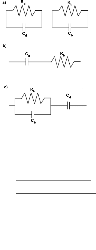
4.3.4 Complex Junction Impedance and Cryogenic Temperatures
The I − V reverse characteristics of the p
+
− n diode, considered in Sects. 4.3.2
and 4.3.3, were derived and also measured under the condition that diode voltages
change so slowly that the excess carrier distributions in the two regions of the junc-
tion remain in a steady state. When a small sinusoidal voltage is superimposed to the
dc bias, the current-voltage behavior cannot be expressed by static characteristics,
because the diode shows a capacitive behavior. Thus, at room temperature, the
diode impedance will be described by accounting for both the ohmic and capacitive
parts of the depleted region (e.g., Section 3.5.2 of [Sze (1985)], Section 9.1 of [Tyagi
(1991)] and Section 4.4 of [Shur (1996)]) and, as a consequence, will depend on the
frequency (f ) of the ac signal. However, the so-called diffusion capacitance
‡‡
can be
neglected, when a reverse voltage is applied. In addition, since at low temperature
the carriers start to freeze-out (see Sect. 4.3.3.3), the capacitance of the field-free
region has been taken into account together with its resistance
∗
in the compre-
hensive model for the Small-signal ac Impedance of a one-sided p
+
− n Junction
Diode (SIJD) operated under reverse bias [Li (1994a); Croitoru, David, Rancoita,
Rattaggi and Seidman (1997a, 1998b)].
The admittance of the equivalent circuit for the SIJD model [Fig. 4.29(a)] is:
Y (ω) =
·
1
Y
d
(ω)
+
1
Y
b
(ω)
¸
−1
=
Y
d
(ω) Y
b
(ω)
Y
d
(ω) + Y
b
(ω)
, (4.148)
where ω = 2πf,
Y
d
(ω) =
1
R
d
+ jωC
d
(4.149)
and
Y
b
(ω) =
1
R
b
+ jωC
b
(4.150)
are the admittances of the depleted and field-free (i.e., the electrical neutral bulk)
regions, respectively; C
d
(R
d
) and C
b
(R
b
) are the capacitances (resistances) of
‡‡
The diffusion capacitance is related to the minority carriers injected into the neutral region
(e.g., Section 9.1 of [Tyagi (1991)] and Section 4.4 of [Shur (1996)]).
∗
One can see, e.g., [Viswanathan, Divakaruni and Kizziar (1991); Divakaruni, Prabhakar and
Viswanathan (1994)].
January 9, 2009 10:21 World Scientific Book - 9.75in x 6.5in ws-bo ok975x65˙n˙2nd˙Ed
Radiation Environments and Damage in Silicon Semiconductors 399
Fig. 4.29 Equivalent circuit for a non-irradiated one-sided junction operated under reverse bias
(from [Leroy and Rancoita (2007)]). C
d
(R
d
) and C
b
(R
b
) are the capacitances (resistances) of the
depleted and field-free regions, respectively: (a) general equivalent circuit, (b) at room temperature
for R
d
À 1/(ωC
d
) and R
b
¿ 1/(ωC
b
), (c) at low temperature for R
d
À 1/(ωC
d
) with ω = 2πf ,
where f is the test frequency.
the depleted and field-free regions, respectively. Introducing Eqs. (4.149, 4.150) in
Eq. (4.148), we obtain
Y (ω) =
(1 + jωC
d
R
d
)(1 + jωC
b
R
b
)
(1 + jωC
d
R
d
)R
b
+ (1 + jωC
b
R
b
)R
d
=
1 − ω
2
C
d
C
b
R
d
R
b
+ jω(C
d
R
d
+ C
b
R
b
)
(R
d
+ R
b
) + jωR
d
R
b
(C
d
+ C
b
)
=
1 − ω
2
C
d
C
b
R
d
R
b
+ jω(C
d
R
d
+ C
b
R
b
)
(R
d
+ R
b
)
2
+ ω
2
R
2
d
R
2
b
(C
b
+ C
d
)
2
×[(R
d
+ R
b
) − jωR
d
R
b
(C
d
+ C
b
)]. (4.151)
Finally, using Eq. (4.151), the admittance of the equivalent circuit for the SIJD
model [Fig. 4.29(a)] becomes:
Y (ω) = G(ω) + j B(ω) (4.152)
=
1
R
r,eff
(ω)
+ j ωC
r,eff
(ω)