Melitz W., Shena J., Kummela A.C., Lee S. Kelvin probe force microscopy and its application
Подождите немного. Документ загружается.


Surface Science Reports 66 (2011) 1–27
Contents lists available at ScienceDirect
Surface Science Reports
journal homepage: www.elsevier.com/locate/surfrep
Kelvin probe force microscopy and its application
Wilhelm Melitz
a,b
, Jian Shen
a,b
, Andrew C. Kummel
a
, Sangyeob Lee
a,∗
a
Department of Chemistry and Biochemistry, University of California, San Diego, La, Jolla, CA 92093, USA
b
Materials Science & Engineering Program, University of California, San Diego, La, Jolla, CA 92093, USA
article info
Article history:
Accepted 18 October 2010
editor: W.H. Weinberg
Keywords:
Kelvin probe force microscopy
Scanning probe miscroscopy
abstract
Kelvin probe force microscopy (KPFM) is a tool that enables nanometer-scale imaging of the surface
potential on a broad range of materials. KPFM measurements require an understanding of both the
details of the instruments and the physics of the measurements to obtain optimal results. The first part
of this review will introduce the principles of KPFM and compare KPFM to other surface work function
and potential measurement tools, including the Kelvin probe (KP), photoemission spectroscopy (PES),
and scanning electron microscopy (SEM) with an electron beam induced current (EBIC) measurement
system. The concept of local contact potential difference (LCPD), important for understanding atomic
resolution KPFM, is discussed. The second part of this review explores three applications of KPFM: metallic
nanostructures, semiconductor materials, and electrical devices.
© 2010 Elsevier B.V. All rights reserved.
Contents
1. Introduction........................................................................................................................................................................................................................ 1
2. Principles of scanning Kelvin probe force microscopy .................................................................................................................................................... 2
2.1. Basic principle of atomic force microscopy ......................................................................................................................................................... 2
2.2. Kelvin probe force microcopy ............................................................................................................................................................................... 3
2.2.1. Fundamentals of KPFM........................................................................................................................................................................... 3
2.2.2. KPFM operational mode: FM and AM mode ......................................................................................................................................... 4
2.2.3. KPFM instrumentation and preparation of conducting AFM tip ......................................................................................................... 5
2.2.4. Comparison of KPFM to other surface potential measurement systems ............................................................................................ 6
2.2.5. High-resolution KPFM: concept of LCPD............................................................................................................................................... 6
3. Application of high-resolution KPFM ............................................................................................................................................................................... 11
3.1. Electrical properties of metallic nanostructures.................................................................................................................................................. 11
3.1.1. KPFM on metallic nanostructures.......................................................................................................................................................... 11
3.1.2. Charge transfer in metallic nanostructure catalyst .............................................................................................................................. 12
3.2. Characterization of electrical properties on semiconductor nanostructures .................................................................................................... 14
3.2.1. KPFM on semiconductor surfaces.......................................................................................................................................................... 14
3.2.2. Adsorbates on semiconductor surfaces................................................................................................................................................. 16
3.3. Nano-scale electrical properties characterization in devices ............................................................................................................................. 17
3.3.1. Quantum dots ......................................................................................................................................................................................... 17
3.3.2. Junctions and heterostructures ............................................................................................................................................................. 18
3.3.3. Transistors............................................................................................................................................................................................... 20
3.3.4. Solar cells ................................................................................................................................................................................................ 23
4. Concluding remarks ........................................................................................................................................................................................................... 26
Acknowledgements............................................................................................................................................................................................................ 26
References........................................................................................................................................................................................................................... 26
1. Introduction
Kelvin probe force microscopy, or KPFM, was introduced as a
tool to measure the local contact potential difference between a
∗
Corresponding author. Tel.: +1 858 534 9505; fax: +1 858 534-2063.
E-mail address: sangyeob@ucsd.edu (S. Lee).
conducting atomic force microscopy (AFM) tip and the sample,
thereby mapping the work function or surface potential of the
sample with high spatial resolution. Since its first introduction
by Nonnenmacher et al. in 1991 [1], KPFM has been used
extensively as a unique method to characterize the nano-scale
electronic/electrical properties of metal/semiconductor surfaces
and semiconductor devices. Recently, KPFM has also been used to
0167-5729/$ – see front matter © 2010 Elsevier B.V. All rights reserved.
doi:10.1016/j.surfrep.2010.10.001
2 W. Melitz et al. / Surface Science Reports 66 (2011) 1–27
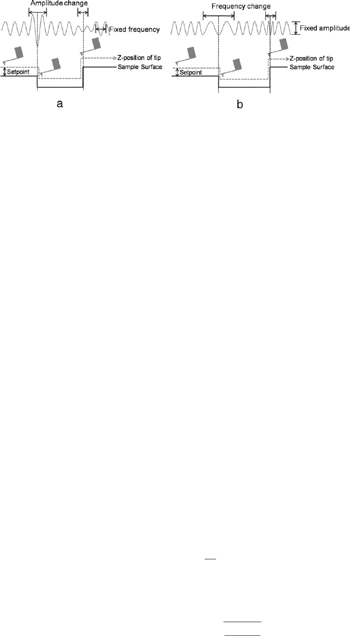
Fig. 1. Schematic depiction of non-contact AFM operation mode: (a) Amplitude modulation mode and (b) Frequency modulation mode. Both AM and FM modes maintain
constant tip–sample separation. AM mode uses oscillation amplitude changes as a feedback signal while FM mode uses frequency changes as feedback signal.
study the electrical properties of organic materials/devices [2–4]
and biological materials [5,6].
This review presents the principles and theory of KPFM
and explores the use of sub-nanometer resolution KPFM to
characterize the electrical properties of metal and semiconductor
materials/devices.
Since the KPFM experimental is an AFM based apparatus, the
basic operational principles and instrumentation of AFM and KPFM
are reviewed together. A comparison is made between KPFM
and other surface potential or work function measurement tools.
Recent reports show that KPFM can be used to image potential
distributions on the surface with sub-nanometer resolution,
making KPFM the best technique, at present, for characterizing the
electrical properties of nanostructures.
KPFM measures a contact potential difference (CPD) between
the sample surface and the tip. In high-resolution KPFM, CPD is
strongly affected by a short-range force between tip and sample.
The CPD associated with the short-range force is specifically
referred as the local contact potential difference (LCPD). For the
high-resolution KPFM, understanding the fundamental difference
between the CPD and the LCPD is critical, as is knowing how the
CPD and LCPD correspond to physical properties of the surface.
Applications of KPFM to electrical property analysis of nanos-
tructures are reviewed in the second part. (1) KPFM character-
ization of the electrical properties of metallic nanostructures is
described. KPFM has enabled the experimental determination of
quantum size effects on the electronic properties of metallic nanos-
tructures. (2) KPFM has been used to study of electronic properties
of semiconductor nanostructures and surfaces. Electronic prop-
erties of defects on clean semiconductor surfaces have been in-
vestigated using sub-nanometer resolution KPFM. High-resolution
KPFM has been successfully applied to the study of a variety
of adsorbates and their interaction with semiconductor surfaces.
(3) High-resolution KPFM has been used to probe semiconductor
devices. A notable application of KPFM is the imaging of opera-
tional electrical devices to provide the high-resolution potential
profiles. These measurements provide critical, near-atomic scale
information on processing induced defects and their effects to the
performance of the electrical devices.
2. Principles of scanning Kelvin probe force microscopy
2.1. Basic principle of atomic force microscopy
KPFM is primarily based on the instrumentation of an AFM
system. AFM operates in contact, intermediate (tapping), and
non-contact modes. In contact mode operation, the AFM tip
touches the sample surface, and the tip–sample repulsive force
deflects the tip–cantilever. The cantilever deflection is monitored
and used as a feedback signal. In intermediate and non-contact
mode, the cantilever is externally oscillated at, or close to, its
resonance frequency. The tip–sample interaction is altered as
the tip–sample distance changes, leading to a change in oscil-
lation amplitude (intermediate mode) and resonance frequency
(non-contact mode). These amplitude and frequency changes, with
respect to the reference amplitude and frequency, are used as feed-
back signals to obtain the topography of the sample surface. There-
fore, intermediate mode and non-contact mode are referred as
amplitude modulation (AM) and frequency modulation (FM) op-
eration, respectively.
In intermediate and non-contact mode AFM, the tip–sample
interaction is perturbed by attractive and repulsive forces, causing
amplitude or frequency changes in the oscillation of the AFM tip,
as illustrated schematically in Fig. 1. In AM mode AFM, changes in
the oscillation amplitude provide the feedback signal for imaging.
As seen in Fig. 1(a), the amplitude of oscillation increases as the
tip–sample distance increases, due to the decrease of tip–sample
interaction. The amplitude change is monitored and regulated by
a feedback system to keep the tip–sample distance constant at a
pre-determined set-point. The dependence of amplitude change
on the tip–sample interaction can be described analytically, based
on the harmonic oscillator model, and the amplitude change is
generally accepted to be dependent on the force between the tip
and sample. Therefore, AM mode measurements represent the
direct force between the tip and sample [7,8].
In FM mode AFM, changes in the oscillation frequency pro-
vide information about tip–sample interactions. The cantilever
oscillation frequency changes due to the tip–sample distance vari-
ation, as illustrated in Fig. 1(b). A feedback system regulates the fre-
quency change to keep the set-point frequency constant, allowing
the topography of the sample surface to be acquired. The changes
in oscillation frequency are dependent on the force gradient be-
tween tip and sample when the restoring force of the cantilever
that is associated with tip oscillating energy is large compared
to the interaction force between the tip and sample surface [8,9].
Therefore, the FM mode AFM detects the force gradient rather than
force itself, a factor enabling FM mode AFM to have higher spatial
resolution than AM mode AFM.
AFM resolution is dependent on the quality factor (Q )of
the vibrating cantilever, a measure of the energy loss of the
oscillation [7]. Q is defined as the ratio between resonant
frequency
(f
0
) and frequency change (f ) at full-width-half-
maximum:
Q
=
f
0
f
. (2.1)
In air, the typical Q of a cantilever, with a resonant frequency of
300 kHz, is approximately 100. The Q in ultra-high vacuum (UHV)
is approximately 50,000, 500 times the Q in air [8]. An expression
for the minimum detectable force
(δF
min
) by an AFM is:
δF
min
=
2k
L
k
B
TB
ω
0
Q
z
2
osc
,
(2.2)
where k
L
is the force constant of the cantilever, k
B
T is the
thermal energy at the ambient temperature, B is the measurement
bandwidth,
ω
0
is the resonant frequency of tip, and
z
2
OSC
is the
W. Melitz et al. / Surface Science Reports 66 (2011) 1–27 3
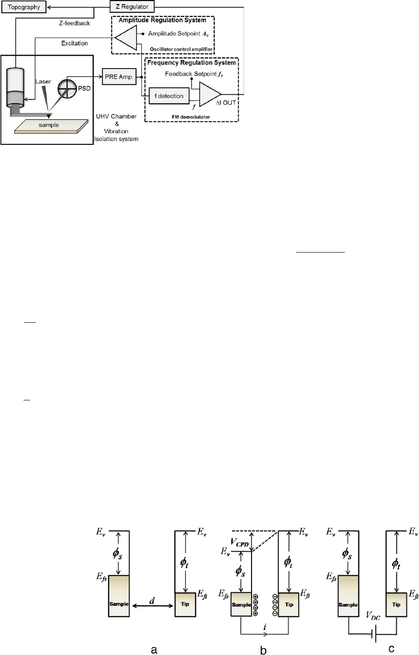
Fig. 2. Block diagram of FM mode AFM system operated in UHV. The piezo scanner
and the laser/PSD are enclosed in a UHV chamber system. The laser signal is
amplified throughthe pre-amp and fed into two feedback systems for the amplitude
and frequency regulation systems. The amplitude is set to a pre-determined set-
point A
0
. The frequency shift (f ) is kept constant to acquire topographic images
of the sample surface.
mean-square amplitude of the driven cantilever vibration [9]. Since
the Q in UHV is 500 times greater than Q in air, the sensitivity
of the AFM system can be 20–25 times greater in UHV than air.
Therefore, it is desirable to operate the AFM in UHV to achieve
high-resolution. However, it is not desirable to operate AM mode
AFM in UHV, since the amplitude change response occurs slowly
with tip–sample interaction due to the increased Q in UHV. The
time scale of amplitude change in AM mode
(τ
AM
) is given by [9]:
τ
AM
≈
2Q
f
0
. (2.3)
The time scale of the amplitude change is linearly dependent on Q
in AM mode AFM. In contrast, the frequency change time response
in FM mode AFM does not depend on Q . The time scale of frequency
change in FM mode
(τ
FM
) is given by [9]:
τ
FM
≈
1
f
0
. (2.4)
Therefore, FM mode AFM operated in UHV, with increased Q ,
results in high-resolution AFM imaging.
An AFM system is typically composed of tip–sample interaction
monitoring (laser and position sensitive detectors) and feedback
systems. Fig. 2 shows the schematic of an FM mode AFM
working in a UHV environment. The amplitude regulation feedback
system and the frequency regulation feedback system are the
two feedback loops in an FM mode AFM system. The amplitude
regulation feedback system keeps the amplitude of the AFM
tip oscillation constant, while the frequency regulation feedback
system maintains the frequency shift (the difference between the
tip oscillation frequency and the set-point frequency) constant
by adjusting the z-position of the AFM tip. The tip oscillation is
monitored by the laser beam movement by a position sensitive
detector (PSD). A pre-amp amplifies the PSD signal. The amplitude
signal of the tip oscillation feeds into the amplitude regulation
system. The amplitude regulation system generally consists of a
positive feedback amplifier, a band-pass filter, and a phase shifter
to detect an amplitude peak and to generate an excitation signal for
cantilever oscillation. Concurrently, the FM demodulator (phase-
locked-loop) measures the oscillation frequency
(f ) and compares
f with the pre-defined set-frequency f
0
[10]. The error signal f −f
0
feeds into the z regulator, which controls the z-position of the tip
to maintain a constant tip–sample interaction by minimizing f
−f
0
.
2.2. Kelvin probe force microcopy
2.2.1. Fundamentals of KPFM
The KPFM measures CPD between a conducting AFM tip and a
sample. The CPD
(V
CPD
) between the tip and sample is defined as:
V
CPD
=
φ
tip
− φ
sample
−e
, (2.5)
where
φ
sample
and φ
tip
are the work functions of the sample and tip,
and e is the electronic charge. When an AFM tip is brought close
to the sample surface, an electrical force is generated between the
tip and sample surface, due to the differences in their Fermi energy
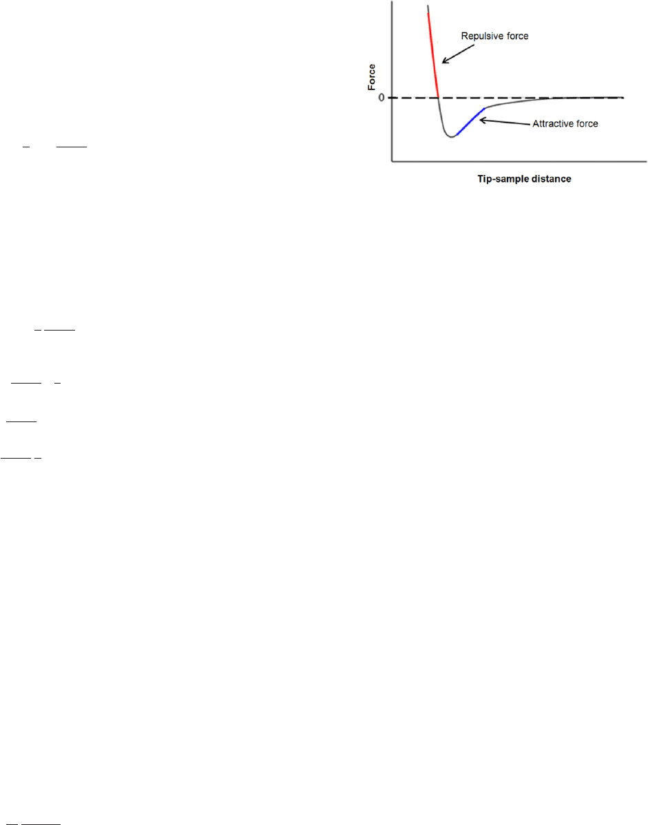
levels. Fig. 3 shows the energy level diagram of the tip and sample
surface when
φ
sample
and φ
tip
are different. Fig. 3(a) depicts the
energy levels of the tip and sample surface when separated by a
distance d and not electrically connected (note, the vacuum levels
are aligned but Fermi energy levels are different). Equilibrium
requires Fermi levels to line-up at steady state, if the tip and sample
surface are close enough for electron tunneling. Upon electrical
contact, the Fermi levels will align through electron current flow,
and the system will reach an equilibrium state, Fig. 3(b). The tip
and sample surface will be charged, and an apparent V
CPD
will form
(note, the Fermi energy levels are aligned but vacuum energy levels
are no longer the same, and a V
CPD
between the tip and sample
has formed). An electrical force acts on the contact area, due to
the V
CPD
. As shown in Fig. 3(c), this force can be nullified. If an
applied external bias
(V
DC
) has the same magnitude as the V
CPD
with opposite direction, the applied voltage eliminates the surface
charge in the contact area. The amount of applied external bias
(V
DC
) that nullifies the electrical force due to the V
CPD
is equal to the
work function difference between the tip and sample; therefore,
Fig. 3. Electronic energy levels of the sample and AFM tip for three cases: (a) tip and sample are separated by distance d with no electrical contact, (b) tip and sample are
in electrical contact, and (c) external bias
(V
dc
) is applied between tip and sample to nullify the CPD and, therefore, the tip–sample electrical force. E
v
is the vacuum energy
level. E
fs
and E
ft
are Fermi energy levels of the sample and tip, respectively.
4 W. Melitz et al. / Surface Science Reports 66 (2011) 1–27
the work function of the sample can be calculated when the tip
work function is known.
By applying an AC voltage
(V
AC
) plus a DC voltage (V
DC
) to the
AFM tip, KPFM measures the work function of the sample. V
AC
generates oscillating electrical forces between the AFM tip and
sample surface, and V
DC
nullifies the oscillating electrical forces
that originated from CPD between tip and sample surface. The
electrostatic force
(F
es
) between the AFM tip and sample is given
by:
F
es
(z) =−
1
2
V
2
dC(z)
dz
, (2.6)
where z is the direction normal to the sample surface,
V is the
potential difference between V
CPD
and the voltage applied to the
AFM tip, and dC/dz is the gradient of the capacitance between tip
and sample surface. When V
AC
sin(ωt) +V
DC
is applied to the AFM
tip, the voltage difference V will be:
V = V
tip
± V
CPD
=
(
V
DC
± V
CPD
)
+
V
AC
sin(ωt). (2.7)
Note that the
± sign depends whether the bias (V
DC
) is applied to
the sample (+) or the tip (−)[11]. Substituting Eq. (2.7) in Eq. (2.6)
gives the expression of the electrostatic force applied to the AFM
tip:
F
es
(z, t) =−
1
2
∂C(z)
∂z
[
(
V
DC
± V
CPD
)
+
V
ac
sin(ωt)
]
2
. (2.8)
This equation can be divided into three parts:
F
DC
=−
∂
C(z)
∂z
1
2
(
V
DC
± V
CPD
)
2
(2.9)
F
ω
=−
∂
C(z)
∂z
(
V
DC
± V
CPD
)
V
AC
sin(ωt) (2.10)
F
2ω
=
∂
C(z)
∂z
1
4
V
2
AC
[
cos
(2ω t) − 1
]
. (2.11)
F
DC
(Eq. (2.9)) results in a static deflection of the AFM tip. F
ω
with frequency ω (Eq. (2.10)) is used to measure the V
CPD
, and F
2ω
can be used for capacitance microscopy [12]. When electrostatic
forces are applied to the tip by V
AC
with V
DC
, additional oscillating
components (due to the electrical force) will be superimposed
to the mechanical oscillation of the AFM tip. A lock-in amplifier
is employed to measure the V
CPD
, to extract the electrical force
component with frequency ω(F
ω
), a function of V
CPD
and V
AC
. The
output signal of the lock-in amplifier is directly proportional to the
difference between V
CPD
and V
DC
. The V
CPD
value can be measured
by applying V
DC
to the AFM tip, such that the output signal of
the lock-in amplifier is nullified and F
ω
equals zero. Subsequently,
the value of V
DC
is acquired for each point on the sample surface,
composing a map of the work function or surface potential of the
whole sample surface area.
Eq. (2.8) is derived from the capacitive energy between
two parallel metal plates, and the equation is valid for CPD
measurements on metallic surfaces. The space-charge-layer (SCL)
on the surface of a semiconductor is well-known, and the effect
of the SCL has to be considered when measuring CPD on a
semiconductor surface. Hudlet et al. analyzed the electrostatic
force in a metallic AFM tip/metallic surface and a metallic AFM
tip/semiconductor surface [13]. In the case of a semiconductor
surface, F
ω
is derived as:
F
ω
=−
Q
s
ε
0
C
I
C
D
C
I
+ C
D
V
AC
sin(ωt), (2.12)
where Q
s
is total charge near the semiconductor surface due to the
surface potential of the semiconductor, ε
0
is the dielectric constant,
C
I
is the capacitance associated with V
ac
and the air gap between tip
and sample, and C
D
is the capacitance associated with V
ac
and SCL
in the semiconductor. For a semiconductor surface, the measured
CPD is related to the surface potential, which differs from the
work function of semiconductor materials, due to the SCL near the
semiconductor surface.
Fig. 4. A typical inter-atomic force vs. distance curve. The force gradient (derivative
of curve) is limited to the short-range in tip–sample distance, while the force is long-
ranged compared to the force gradient.
2.2.2. KPFM operational mode: FM and AM mode
As previously described, AFM can detect atomic forces by AM or
FM mode. The electrostatic force F
ω
can also be detected either by
AM or FM mode in KPFM. AM mode KPFM measures F
ω
directly
from the amplitude of the cantilever oscillation at
ω induced
by V
CPD
and V
AC
. V
DC
is applied to the AFM tip to nullify the
measured amplitude, thereby measuring V
CPD
. In FM mode KPFM,
F
ω
is detected by the frequency shift at ω, and V
DC
is applied to the
AFM tip to nullify the frequency shift, thereby measuring V
CPD
.
KPFM measures topography concurrently with V
CPD
, using an
AFM tip. A method to separate the topographical signal from
the V
CPD
measurement is required. In the KPFM experimental
setup, the V
AC
is usually modulated at a frequency higher than
the bandwidth of the topography feedback system to prevent
cross-talk between topography and CPD measurement. In AM
mode KPFM, topography is measured by the oscillation at the first
resonance frequency of the AFM tip, and V
CPD
is measured by the
amplitude of the oscillation at the second resonance frequency
of the AFM tip. A mechanically vibrated cantilever generally has
several resonance peaks in the oscillation amplitude–frequency
spectrum. The second resonance peak normally has a broader
peak than the first resonance frequency peak. The amplitude
of the second resonance peak is usually less than one-third of
the first resonance frequency peak, and the frequency of the
second resonance peak is typically 6 times the first resonance
frequency [14]. V
AC
is tuned to the second resonance frequency
to excite the AFM tip by electrical force, while the first resonance
frequency is assigned for the tip height control. Using these
techniques, the topography and the V
CPD
signal can be separated.
Conversely, in FM mode KPFM, the AFM tip is mechanically excited
at the first resonance frequency. V
AC
induces a modulation of
the electrostatic force, which is detected by the superimposed
oscillation at the frequency variation of the mechanical oscillation
of the AFM tip, leading to the separation of topography and V
CPD
signal.
The spatial resolution of measuring V
CPD
in FM mode KPFM is
higher than in AM mode KPFM. Similar to the AM and FM mode
AFM, the AM mode KPFM directly detects the electrostatic force by
the oscillation of the cantilever, but the FM mode KPFM detects the
electrostatic force gradient by the frequency shift of the cantilever
oscillation, which contributes to greater spatial resolution [14,15].
However, the detection range of the force gradient is shorter-
ranged than the force itself, which is explained by the inter-atomic
force–distance curve.
Fig. 4 shows the typical force–distance curve. In the at-
tractive force regime, the force gradient (the derivative of the
force–distance curve) becomes larger when the inter-atomic dis-
tance is small. As the inter-atomic distance increases, the force
gradient becomes insignificant. Therefore, the detection of force
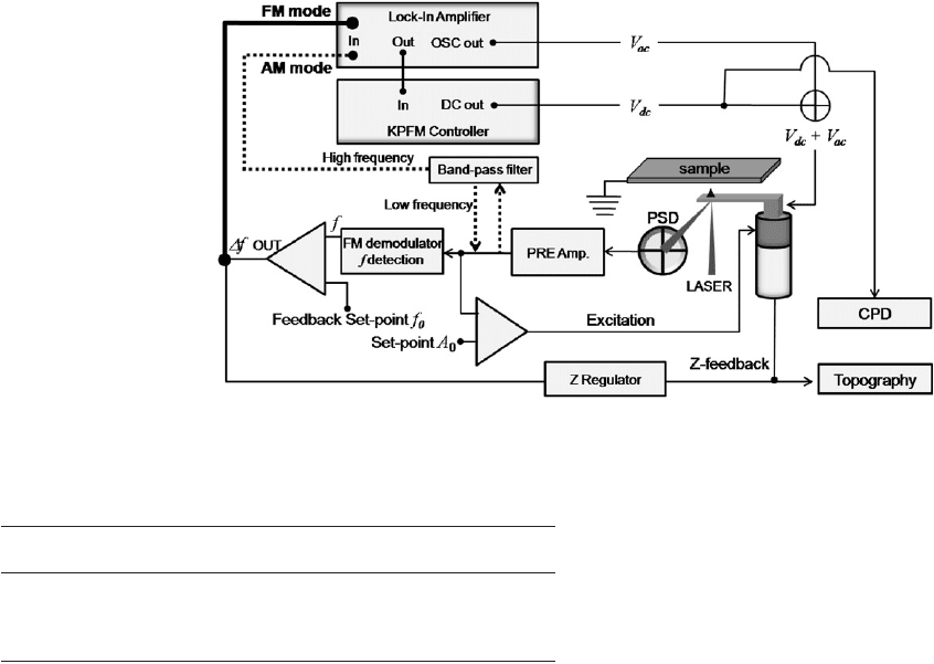
W. Melitz et al. / Surface Science Reports 66 (2011) 1–27 5
Fig. 5. Schematic diagram of KPFM system showing AM and FM mode. Lower part of the diagram is an FM mode AFM system for topography imaging and upper part is a
KPFM system for CPD measurement.
Table 1
Typical spatial and energy resolution of FM and AM mode KPFM.
KPFM
mode
Spatial resolution Energy resolution
(meV)
FM Possibly sub-nanometer resolution depending
on tip apex
10–20
AM Typically 25 nm (sub-nanometer resolution also
possible depending on sample)
5
gradient mainly takes place at the end of the AFM tip. Conse-
quently, the detection of electrostatic force is considered long-
range detection, whereas the detection of electrostatic force
gradient is short-range detection. The electrostatic interaction
takes place mainly between the tip apex and sample surface in the
FM mode KPFM. The spatial resolution is approximately equal to
the dimension of the tip apex in the FM mode KPFM. However, the
electrostatic interaction from the sample includes both the tip and
the cantilever in AM mode KPFM due to the long-range detection
scheme. As a result, the spatial resolution of AM mode KPFM is re-
duced by an averaging effect between the tip and cantilever.
Although FM mode KPFM is generally considered to have better
spatial resolution than AM mode, it has been demonstrated that
AM mode can also show the atomic-scale resolution in KPFM
images [16]. The aforementioned comparison of spatial resolution
of FM and AM mode KPFM includes only long-range electrostatic
interaction. However, recent theoretical studies on the limitation
of FM and AM mode KPFM suggested that the short-range
interaction becomes more significant in atomic-scale KPFM and
both FM and AM mode KPFM in the sub-nanometer regime have
the same limitation in spatial resolution (see Section 2.2.5)[17].
The energy resolution of measurements of V
CPD
in AM mode
KPFM is higher than in FM mode KPFM. AM mode KPFM measures
the V
CPD
from the resonance peak of the oscillating cantilever
greatly enhancing the signal-to-noise ratio [14,18]. Conversely, FM
mode KPFM detects the V
CPD
through an FM demodulator [14], and
additional noise is generated, when the signal passes through the
FM demodulator. Consequently, the energy resolution of AM mode
KPFM is superior, due to the high signal-to-noise ratio compared to
FM mode KPFM. The typical spatial and energy resolutions of V
CPD
measurement by FM and AM mode KPFM are listed in Table 1.
2.2.3. KPFM instrumentation and preparation of conducting AFM tip
Fig. 5 shows the schematic diagram of a KPFM experimental
apparatus. The lower part shows the FM mode AFM system
for topography measurement, and the upper part shows the
components for CPD mapping, including the KPFM controller and
lock-in amplifier. The dashed line and bold straight line in the
diagram show the AM and FM mode KPFM configurations. V
ac
is applied to the tip from the lock-in amplifier reference signal
voltage output (OSC out). In FM mode, the frequency shift signal
(f ) is split into two; one goes to the z regulator for topographic
imaging, and the other is fed into the lock-in amplifier. The lock-
in amplifier extracts the signal with the same frequency as V
ac
and feeds the signal into the KPFM controller. The KPFM controller
maintains feedback to nullify the lock-in output signal, by applying
V
dc
to the tip. In AM mode, V
ac
with the same frequency as the
second resonant peak of tip oscillation is applied to the AFM tip to
excite the tip with electrical force. The amplitude of tip oscillation
has two components; low frequency (the first resonance peak)
tuned by mechanical oscillation and high frequency (the second
resonance peak) tuned by V
ac
. A band-pass filter filters the low
and high frequency signals. The low frequency signal is used for
topography regulation. The high frequency signal feeds directly
into the lock-in amplifier. The KPFM controller measures CPD using
the second resonance frequency component.
The preparation of atomically sharp and conducting AFM
tips is critical for high-resolution KPFM. An AFM tip can be
prepared for high-resolution KPFM using any of several methods.
(a) The most common method is to take a commercially available
heavily doped Si cantilever and use heat treatment followed
by Ar
+
bombardment to remove the native oxide layer and
other contaminants [19–21]. These tips routinely produce high-
resolution images, but are more likely to pick up surface atoms,
altering the work function of the tip. (b) Some commercially
available tips, for example, Pt/Ir-coated Si cantilevers, can produce
sub-nanometer resolution KPFM images [16,22]. The commercial
Pt/Ir-coated tips do not require substantial tip preparation, but
yield lower spatial resolution. (c) HF wet etching of Si tips followed
by a high temperature annealing has also been successful for high-
resolution KPFM imaging [23]. Etching Si tips is an alternative
method to ion bombardment to remove the native oxide. (d) The
coating of Si cantilevers with a very thin Au or Cr layer (typically a
few nm thick) also produces high-resolution KPFM images [24,25].
Cr-coated tips are less reactive so that they have a more stable
tip work function. Obtaining the best spatial resolution requires
optimization of the tip coating film thickness. (e) UHV field
emission tip cracking can produce sub-nanometer resolution. A
tungsten filament is positioned close to the cantilever, and a high
voltage is applied between the tungsten filament and the AFM tip.
Electrons tunneling from the filament to the tip remove the native

6 W. Melitz et al. / Surface Science Reports 66 (2011) 1–27
Table 2
Comparison of Kelvin probe force microscopy, Kelvin probe method, photoemission spectroscopy, and scanning electron microscopy to measure the surface potential.
Method Description Energy resolution Spatial resolution
KPFM Measuring local CPD of the sample surface 5–20 meV Better than 10 nm [24]
KP Measuring CPD of the whole sample surface 1 meV Averaging a whole sample surface
PES Measuring energy spectroscopy of the whole sample surface 20 meV [29] Better than 100 nm [29]
SEM Measuring electron beam induced current to map the surface potential Not a quantitative method Better than 70 nm [30]
oxide. (f) The simplest method to make a conducting silicon AFM
tip is gently touching the AFM tip end into the sample surface,
removing the native oxide [26,27].
2.2.4. Comparison of KPFM to other surface potential measurement
systems
The surface potential or work function of a sample can
also be measured by various techniques such as Kelvin probe
(KP), photoelectron spectroscopy (PES), and scanning electron
microscopy (SEM) with electron beam induced current (EBIC)
analysis. Similar to KPFM, the KP also measures the CPD between
the probe and sample surface. The working principle of KPFM and
the KP are similar, but the KP is an averaging method including
the CPD values of the whole sample area which does not provide a
map of the CPD on the sample surface. PES measures the energy
of photo-stimulated electrons emitted from a sample surface.
Angle resolved high resolution PES can be used to determine the
electronic band structure of the sample. SEM can also resolve the
local electronic structure of the semiconductor sample surface by
measuring EBIC [28].
When semiconductor sample surfaces are bombarded by
energetic electrons (typically several keV), electron–hole pairs are
generated. The generated electrons and holes are free to move in a
sample. In the absence of any local electric fields, these electrons
and holes move randomly and typically recombine. When local
electric fields exist within a semiconductor sample, the local
electric fields can separate the electrons and holes, and EBIC can
flow throughout the sample. The EBIC is linearly dependent on
the local electric field on the sample surface. The surface potential
of a sample (as a function of the local electric field) is mapped
by monitoring the EBIC signal during the scanning of the electron
beam over the sample surface.
The spatial resolution of KPFM is higher than of the PES and
EBIC methods. The sensitivity of KPFM in measuring either the
surface potential or work function is comparable to PES but
less than KP. Typically, laboratory scale PES has been used to
measure the electronic band structures of the whole sample
surface. The spatial resolution has improved gradually to 3
μm,
due to improvements in the photon source and electron energy
analyzer. When synchrotron radiation sources are used for PES, a
spatial resolution better than 100 nm is possible [29].
The spatial resolution of EBIC technique can be 70 nm [30].
However, the EBIC technique has some disadvantages in measuring
the surface potential of samples. The technique can only be applied
to a semiconductor sample, since EBIC measures the current
generated from electron–hole pairs. In addition, the absolute
surface potential is difficult to quantify, since the correlation
between EBIC and surface potential values is not physically
defined. Table 2 summarizes the spatial and energy resolution of
KPFM, KP, PES, and SEM.
Although KPFM has superior spatial resolution with relatively
high energy sensitivity compared to other measurement tech-
niques, KPFM has some disadvantages in measuring the abso-
lute surface potential or work function of a sample. First, the
absolute measurement of surface potential using KPFM requires
measurement of the work function of the probe. This requires the
calibration of KPFM probe on a sample with a well-defined work
function. Therefore, two measurements are needed, one on the ref-
erence surface and one on the sample. The necessary exchange of
the two samples under the KPFM probe decreases the accuracy of
the measurement [31]. PES and SEM do not require calibration of
the probe when measuring the surface potential or capacitance of
a sample surface.
Second, KPFM can only measure the molecularly averaged
surface potential changes when a semiconductor sample surface
contains absorbents. KPFM measurements cannot distinguish the
contributions of surface band bending and surface dipoles created
by absorbents from the semiconductor surface [31,32].
PES techniques can provide the entire spectral distribution
of the surface potential allowing determination of the complete
electronic band structure of a sample surface. By comparing PES
measurements of the electronic band structures of a clean surface
and a surface with absorbents, band bending and surface dipole
contributions can be independently determined [31–33].
Third, an abrupt topographic height change can disrupt the
accurate measurement of KPFM. KPFM requires keeping the
tip–sample distance constant during measurement to avoid the
contribution of capacitance gradients (see Eq. (2.6)) to the surface
potential (see the Eq. (2.10))[1,14,18,34]. When a sudden change
in a topographic height during KPFM measurement occurs, the
capacitance gradient term in Eq. (2.10) can change. The change of
capacitance gradient can contribute to the electrical force between
the tip and sample. Consequently, the measured surface potential
value does not always represent of the contact potential between
the tip and sample. In contrast, the surface potential measured by
KP, PES and SEM does not depend on the tip–sample distance.
Fourth, KPFM requires a relatively long time to acquire an image
of a sample surface potential (typically one or two hours). KPFM
measures the surface topography and potential at the same time
using one AFM tip. When the tip is scanned on a sample surface
at high speed, severe cross-talk between topographic and surface
potential signals can be generated [14]. Consequently, the scan-
bandwidth of the topography and surface potential regulation is
limited to avoid the cross-talk. High resolution PES is also very
slow.
2.2.5. High-resolution KPFM: concept of LCPD
In the past decade, atomic-resolution KPFM was demonstrated
on a variety of surfaces, including semiconductors and ionic solids.
The CPD in Eq. (2.5) is based on the capacitive force between
two macroscopic parallel metallic electrodes, which, do not have
lateral electrostatic force distributions at the atomic-scale. In
atomically resolved KPFM, the measured CPD is defined as LCPD,
which depends on the electrostatic interaction on the atomic-
scale. The LCPD is based on the Wandelt’s concept of a local work
function, which illustrates the short-ranged (along the direction
normal to surface) atomic scale variation of work function on
metal surfaces [35]. Similar to the local work function concept,
atomic-scale KPFM measurements of the total electrostatic force
includes a new term (a bias dependent short-range force), which
induces the atomic LCPD contrast. All published theories of LCPD
attribute the atomic-scale contrast of CPD to a short-range force,
due to the microscopic interaction between the apex of the tip and
surface atoms. For ionic solids, the tip–sample interaction resulting
in atomic contrast is the ionic bonding force (dipole interactions)
W. Melitz et al. / Surface Science Reports 66 (2011) 1–27 7
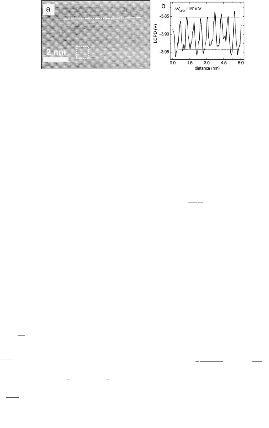
Fig. 6. Atomic resolution KPFM image of KBr(001) surface. (a) CPD image of KBr(001) surface measured by AM mode KPFM in UHV. (b) Line trace of CPD indicated by the
dash line in (a). 97 mV LCPD is clearly observed between K
+
and Br
−
. The dashed box indicates unit cell.
Source: Adapted from [21].
between the surface atom and the tip apex atom. In semiconductor
surfaces, the short-range force is attributed to a covalent bonding
interaction. The origin of the short-range force is highly dependent
on the system. In different systems, different short-range forces
can dominate over the other forces. The dominant short-range
force is minimized by applying a potential to the tip, causing the
LCPD contrast.
2.2.5.1. LCPD in ionic solids. Bocquet et al. reported atomic-
resolution KPFM results on ionic solids such as KBr(001) [21]. Fig. 6
shows the atomically resolved CPD images of KBr(001) surface. The
LCPD between K
+
and Br
−
shows a clear 97 mV difference. Bocquet
et al. also developed an analytical model describing the short-
range electrostatic force between a conducting AFM tip and an
ionic crystal, and showed the short-range electrostatic interaction
between the microscopic tip-end and the local charge distribution
on the ionic crystal surface can account for the LCPD.
Based on the analytical model developed by Bocquet et al.,
Nony et al. also suggested an analytical model of short-range
electrostatic forces which creates the LCPD contrast on ionic
crystals by AM and FM mode KPFM [17]. An interaction of atoms on
the tip apex with the surface provides a lateral force distribution at
the atomic scale. However, the LCPD has a dependence on the tip
geometry, tip–sample distance, and bias between tip and sample.
The short-range electrostatic force is divided into two separate
terms. F
(1)
mμ
represents the interaction between the microscopic tip
apex (which acts as a capacitor with the sample surface) and the
sample counter electrode. F
(2)
μ
represents the force between the
mesoscopic tip apex with the surface charge density caused by
applied bias and the sample. The expression for the total short-
range electrostatic force is [17]:
F
es
(V
applied
, z) = F
(1)
mμ
+ F
(2)
μ
= C
1
(V
applied
(t) − V
CPD
)e
−α z
+[C
0
+ C
2
(V
applied
(t) − V
CPD
)
2
]e
−2 α z
, (2.13)
where
α = 2
√
2π/a and a is the lattice constant of sample surface.
The coefficients are defined as:
C
0
=−
2R
2
q
2
ε
0
a
4
A
(2)
e
−2 α R
a
(2.14)
C
1
=−
6R
2
a
q˜ε
d
a
2
R
D
(1)
e
−α R
a
cos
4π x
0
a
√
2
+ cos
4π y
0
a
√
2
(2.15)
C
2
= C
0
4πχ
d
aqR
2
, (2.16)
where ε
0
is vacuum dielectric permittivity, ˜ε
d
is the effective
dielectric permittivity (for KBr
˜ε
d
= 4.38) and χ
d
is the dielectric
susceptibility (for KBr
χ
d
= 9 × 10
−39
Fm
2
). R (typically larger
than 5 nm) is the mesoscopic tip radius, and R
a
is the microscopic
tip apex radius. A
(2)
(typically −8) and D
(1)
(typically −15) are
integral coefficients [21]. The relative positions of the anion and
the cation are x
0
= y
0
= 0 and x
0
= y
0
= a
√
2/4, respectively.
The coefficient C
1
contains the spatial components (x
0
and y
0
),
whereas C
0
and C
2
are not related to spatial variation. Therefore,
F
(1)
mμ
contributes to the atomic LCPD contrast, and F
(2)
μ
is a static
offset.
Based on the local electrostatic force caused by LCPD, Nony
et al. also proposed an analytical model correlating the external
bias and LCPD in FM and AM mode KPFM, using a nonlinear
equation of motion [17]. The force equation, including the short-
range interaction, translates to an additional term in the measured
CPD. The analytical expression for the measured LCPD in FM and
AM mode KPFM has been derived as follows [17]:
V
LCPD
= V
CPD
−
C
1
2C
2
a
n
b
n
e
α z
min
, (2.17)
where a
n
and b
n
are Fourier coefficients and z
min
is the minimum
tip–sample distance. It should be noted that by only including
the short-range electrostatic forces that LCPD diverges at large
tip–sample separations. The order of the Fourier coefficients is
dependent on the mode of operation of the KPFM. The coefficients
are zero-order (a
0
= 0.1155 and b
0
= 0.0724) for AM mode. The
coefficients are first-order (a
1
= 0.1080 and b
1
= 0.0766) for FM
mode. The difference in coefficients is responsible for the variation
in the measurements between AM and FM mode KPFM. The
difference between AM and FM is expected to be small because the
a to b ratios are nearly the same. Nony et al. also extend this model
to include the long-range electrostatic force. Experimentally, long-
range electrostatic forces accompany the short-range electrostatic
forces.
The full force expression, including both the short-range and
long-range electrostatic interaction, is expressed as [17]:
F
es
(V
applied
, z) = F
(1)
mμ
+ F
(2)
μ
+ F
M
, (2.18)
where F
M
is the macroscopic electrostatic force in terms of z
(the direction normal to sample surface). F
M
is the macroscopic
electrostatic force [17]:
F
M
(V
applied
, z) =−
1
2
S
ε
0
˜ε
2
d
(z
M
+ z)
2
V
applied
−
CPD
e
2
, (2.19)
where S is the surface area of the tip and z
M
is the height of the tip,
with approximate values of S
= 1mm
2
and z
M
= 5 mm. ε
0
and
ε
d
are the dielectric constant of vacuum and the relative dielectric
constant.
The compensated potential difference required to minimize the
total electrostatic force, including the macroscopic long-range and
the short-range electrostatic forces for FM mode KPFM is [17]:
V
(c)
DC
= V
CPD
−
C
1
a
1
e
−αz
min
2C
2
b
1
e
−2αz
min
+ 2π Sε
0
˜ε
2
d
A
0
z
3
M
, (2.20)
8 W. Melitz et al. / Surface Science Reports 66 (2011) 1–27
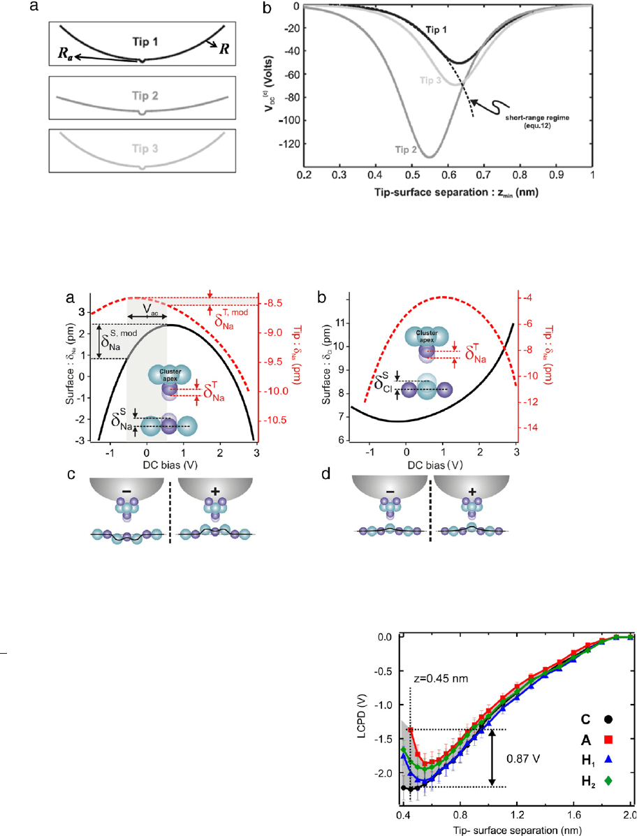
Fig. 7. Compensated potential difference vs. tip–sample distance. (a) Models of the three tips used for the analytical and numerical calculation. The parameters (R, R
a
) in Å
are: tip 1 (50, 1); tip 2 (120, 1.5); tip 3 (50, 1.1). R (typically larger than 5nm) is the mesoscopic tip radius, and R
a
is the microscopic tip apex radius. (b) The total potential
difference
(V
(c)
DC
) for tip 1 (black), tip 2 (dark grey) and tip 3 (light grey). The dotted line indicated the short-range regime. The curves indicate an optimal tip–sample distance
for LCPD contrast.
Source: Adapted from [17].
Fig. 8. Atomic movement of the tip and sample vs. position and applied bias. (a) Movement vs. dc bias when tip positioned 0.45 nm above the Na
+
surface atom. The
solid line is the surface movement
δ
T
Na
. The dashed line is the tip displacement δ
S
Na
, where the positive movement is up towards the tip. (b) Movement vs. dc bias when tip
positioned 0.45 nm above the Cl
−
surface atom. The solid line is the surface displacement δ
T
Cl
. The dashed line is the tip displacement δ
S
Cl
. (c) Model illustrating the atomic
displacement for positive and negative tip bias when positioned above a surface Na
+
atom or (d) Cl
−
atom.
Source: Adapted from [36].
where A
0
is the vibration amplitude of the cantilever, and
α = 2
√
2π/a with a being the lattice constant of the crystal.
The compensated potential difference is the theoretical value
applied to minimize the force accounting for tip geometry and
tip–sample distance. By including the long-range electrostatic
forces, the divergence observed in Eq. (2.17) disappears. Fig. 7
shows the compensated potential difference for the three different
tip geometries. The curves indicate a resonant behavior between
the short-range and long-range regimes. The resonance behavior
implies an optimal tip–sample distance, which amplifies the forces
responsible for the LCPD contrast. An optimal tip–sample distance
is observed experimentally [16,19,23,36].
Using an atomic force microscope simulator, Nony et al.
showed details of the interaction behavior of the cluster of atoms
(microscopic apex) and the surface atoms of NaCl (001) [36]. The
simulated microscopic apex used a Na atom as the apex atom. Both
the tip apex atom and surface atoms could be spatially perturbed
depending on tip position and biasing. With the tip positioned
above a Na
+
surface atom at zero bias, the Na atom on the tip
moves 0.085 Å towards the surface and the surface Na
+
atom
moves 0.02 Å towards the tip. With tip positioned above the
Cl
−
surface atom, the Na atom on the tip moves 0.06 Å towards
Fig. 9. Calculated LCPD vs. Z spectroscopy curves. Four different sites on NaCl
surface (C: on top of Na
+
, A: on top of Cl
−
, H
1
and H
2
: hollow sites between Na
+
and
Cl
−
). The distance dependence on the difference in the measured LCPD indicates an
optimal tip–sample distance for LCPD contrast.
Source: Adapted from [36].
the surface and the Cl
−
surface atom moves 0.07 Å towards the
tip. Fig. 8 shows the atomic motion dependence on tip biasing.
The movement of the atoms is caused by the equilibrium of two
W. Melitz et al. / Surface Science Reports 66 (2011) 1–27 9
Fig. 10. Sub-nanometer resolution FM mode KPFM on InAs(001)-(4 × 2) surface. (a) LCPD and (b) topography of InAs(001)-(4 × 2) surface. (c) Average line profiles of
topography and LCPD. The line profiles are averaged over the area indicated by white lines on (a) and (b). (Experimental results performed by authors.)
separate interactions, the chemical interaction of the apex tip
with the surface and the electrostatic interaction of the tip with
the local surface area. Calculated force-z spectroscopy at four
different positions on the NaCl surface illustrates the tip–sample
dependence on the LCPD contrast. Fig. 9 shows the calculated
dependence of the tip–sample distance on the contrast between
different positions on the NaCl surface. The force-z curves for
position A and C have a drastic change around 0.4 nm tip–sample
separation. The curves indicate a separation of 0.45 nm generates
the contrast of 0.87 V. The existence of an optimal tip–sample
separation is consistent with the previous discussed experiments
for KBr.
For ionic solids, the measured LCPD is a combination of
short-range and long-range electrostatic interactions. The short-
range electrostatic interactions appear to originate from the ionic
interactions of the tip apex with the surface position directly under
the tip and the microscopic electrostatic influence of the tip on the
ionic surface. Theoretical calculations support the tip conditions
needed to achieve LCPD contrast includes the microscopic apex
radius, the mesoscopic tip radius, and the tip–sample distance.
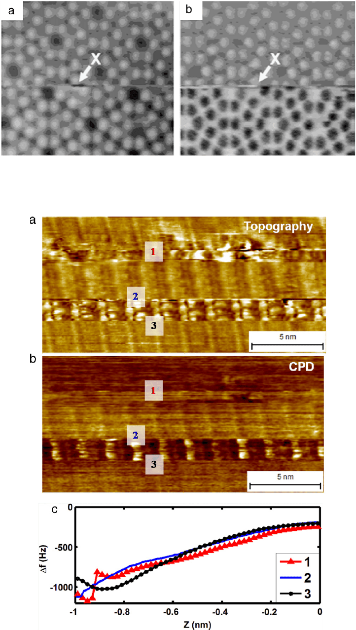
2.2.5.2. LCPD in semiconductors. Sub-nanometer resolution LCPD
has also been observed on a variety of semiconductor surfaces
including: Si [19,20,24,26,37,38], TiO
2
[16,22,39], InSb [23]. Fig. 10
shows simultaneously obtained CPD and topography images of
InAs(001)-(4
× 2) surface using FM mode KPFM (note that the
experimental results in Fig. 10 were performed by the authors).
InAs(001)-(4
×2) has a row-trough structure consisting of In rows
of atoms and pairs of In dimers located in the trough [40]. The
trough region has LCPD peaks. The bulked dimers in the trough
probably cause the LCPD in the trough. The LCPD peaks indicate
a change in the tip–sample interaction.
Okamoto et al. [41] proposed a model to explain the LCPD
contrast on a Si(111)-(7
× 7) surface including contrast reversal
upon tip conditioning, previously reported by Shiota et al. [38].
Fig. 11 shows atomically-resolved topography and CPD images of
a Si(111)-(7
× 7) surface [38]. Fig. 11(b) shows a contrast reversal
at the position indicated with X, where the bright spots become
dark. Okamoto et al. separated the electrostatic force
(F
ES
) from the
topographical force
(F
top
), where the F
ES
is a function of frequency
and F
top
is a function of frequency and applied bias (V
DC
) [41]. The
measured LCPD is affected by the sum of the two forces. The F
top
displays cubic-root-like dependence on V
applied
. The resulting sum
of the F
ES
and F
top
generates multiple intersects with zero force,
meaning multiple stable LCPD values. The derived expression for
the two new stable points is [41]:
V
DC
= V
CPD
±
f
top
(ω, V ) cos θ
(∂C/∂z)V
AC
, (2.21)
where f
top
is the modulation component of the topographical force,
V
AC
is applied AC potential, C is the capacitance, and θ is the
phase difference between the F
ES
and F
top
signals. A spectroscopy
experiment on the Si(111)-(7
× 7) surface by Arai et al. shows
the presence of two separate minimums in the frequency shifts
versus sample bias [19], supporting the Okamoto’s model of
LCPD on semiconductors. The model denotes f
top
(ω) as the short-
range force responsible for the LCPD contrast. The short-range
force is derived from the apex atom’s interaction strength with
the surface. The difference between semiconductor and ionic
materials is the origin of the short-range force, or the bonding
force. The characterization of the short-range force as a covalent
bonding interaction for semiconductors is consistent with previous
experimental studies of Au clusters on Si. The Au clusters shows
higher potential than underlying Si substrate, due to a weaker
bonding of Au–Si compared to Si–Si interactions [26]. The model
is also consistent with the experiments where the LCPD is used for
atom identification on a mixed Si–Sb surface [20].
10 W. Melitz et al. / Surface Science Reports 66 (2011) 1–27
Fig. 11. Atomically-resolved KPFM images of Si(111)-(7 × 7) with contrast reversal. (a) Topography and (b) CPD of Si(111)-(7 × 7) surface. X indicates the location of a
spontaneous contrast reversal.
Source: Adapted from [38].
Fig. 12. Tip conditioning for LCPD contrast. (a) Topography and (b) LCPD images of InAs(001)-(4 ×2) surface. The contrast changes at position 1, 2 and 3. At positions 1 and
2, the tip gently touched the surface rearranging the apex of the cantilever, causing the LCPD contrast change. The LCPD contrast spontaneously reverses due to the tip-state
change. (c) df
(z) spectroscopy curves at points 1, 2 and 3 showing force–distance dependence changes induced by different tip state. (Experimental results performed by
authors.)