Yeang K., Woo L. Dictionary of Ecodesign: An Illustrated Reference
Подождите немного. Документ загружается.

Polycrystalline cells are more cost-efficient
to produce, but are less efficient than mono-
crystalline cells.
Amorphous or thin-layer cells are made up
of a silicon fi lm adhered to glass or other
material. They are the least efficient and
least expensive of the three types of cell.
Because of this, they are primarily used in
low-power equipment (watches, pocket cal-
culators) or as façade elements. Their effi-
ciency is half that of crystalline cells, and
they degrade with use.
Photovoltaic device Solid state electrical
device that converts light into direct current
electricity. The voltage–current characteristics
are a function of the light source, and of the
materials and design of the device. Solar PV
devices are made of various semiconductor
materials including silicon, cadmium, sulfide,
cadmium telluride, and gallium arsenide, and
in single crystalline, multi-crystalline, or amor-
phous forms. The structure of a PV device
depends on the materials used in the PV cells.
There are four basic device designs: i) homo-
junction; ii) heterojunction; iii) p–i–n/n–i–p; and
iv) multijunction.
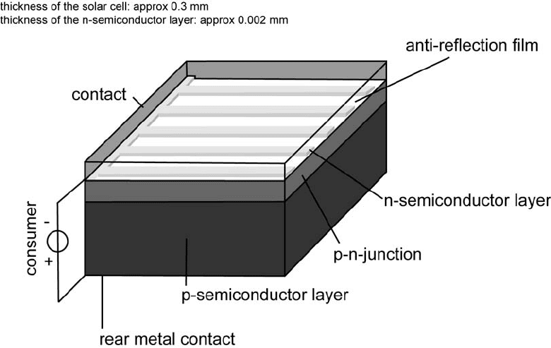
Homojunction device Crystalline silicon is the
primary example of this kind of cell. A single
material—crystalline silicon—is altered so that
one side is p-type, dominated by positive holes,
and the other side is n-type, dominated by
negative electrons. The p/n junction is located
so that the maximum amount of light is absor-
bed near it. The free electrons and holes gener-
ated by light deep in the silicon diffuse to the p/
n junction, then separate to produce a current if
the silicon is of sufficiently high quality.
Some homojunction cells have been designed
with the positive and negative electrical con-
tacts on the back of the cell. This geometry
Figure A.4 Model of a crystalline solar cell
Source: Us Department of Energy
278 Photovoltaic device
eliminates shadowing caused by the electrical
grid on top of the cell. A disadvantage is that
the charge carriers, which are mostly generated
near the top surface of the cell, must travel fur-
ther—all the way to the back of the cell—to
reach an electrical contact. To be able to do
this, the silicon must be of very high quality,
without crystal defects that cause electrons and
holes to recombine.
Heterojunction device An example of this type
is a CIS cell, where the junction is formed by
contacting two different semiconductors—cadium
sulfide (CdS) and copper indium diselenide
(CuInSe
2
). This structure is often chosen for pro-
ducing cells made of thin-film materials that
absorb light much better than silicon. The top
and bottom layers in a heterojunction device
have different roles. The top layer, or window
layer, is a material with a high bandgap selected
for its transparency to light. The window allows
almost all incident light to reach the bottom
layer, which is a material with low bandgap that
readily absorbs light. This light then generates
electrons and holes very near the junction, which
helps effectively to separate the electrons and
holes before they can recombine. Heterojunction
devices have an inherent advantage over homo-
junction devices, which require materials that
can be doped both p-type and n-type. Many PV
materials can be doped either p-type or n-type,
but not both. Again, because heterojunctions do
not have this constraint, different PV materials
can be investigated to produce optimal cells.
Also, a high-bandgap window layer reduces the
cell’s series resistance. The window material
can be made highly conductive, and the thickness
can be increased without reducing the trans-
mittance of light. As a result, light-generated
electrons can easily flow laterally in the window
layer to reach an electrical contact.
p–i–n and n–i–p device Usually, amorphous
silicon thin-film cells use a p–i–n structure,
whereas cadmium telluride (CdTe) cells use an
n–i–p structure. The basic process is: a three-
layer sandwich is created, with a middle intrin-
sic (i-type or undoped) layer between an n-type
and a p-type layer. This geometry sets up an
electric field between the p-type and n-type
regions, which stretches across the middle intrin-
sic resistive region. Light generates free elec-
trons and holes in the intrinsic region, which are
then separated by the electric field. In the p–i–n
amorphous silicon (a-Si) cell, the top layer is
p-type a-Si, the middle layer is intrinsic silicon,
and the bottom layer is n-type a-Si. Amorphous
silicon has many atomic-level electrical defects
when it is highly conductive. So very little cur-
rent would flow if an a-Si cell had to depend on
diffusion. However, in a p–i–n cell, current flows
because the free electrons and holes are gener-
ated within the influence of an electric field,
rather than having to move toward the field. In
a cadmium telluride (CdTe) cell, the device struc-
ture is similar to the amorphous silicon (a-Si)
cell, except that the order of layers is flipped
upside down. Specifically, in a typical CdTe cell,
the top layer is p-type cadmium sulfide
(CdS),
the
middle layer is intrinsic CdTe, and the bottom
layer is n-type zinc telluride (ZnTe).
Multijunction device This structure, also
called a cascade or tandem cell, can achieve a
higher total conversion efficiency by capturing a
larger portion of the solar spectrum. In the typi-
cal multijunction cell, individual cells with dif-
ferent bandgaps are stacked on top of one
another. The individual cells are stacked in such
a way that sunlight falls first on the material
having the largest bandgap. Photons not absor-
bed in the first cell are transmitted to the second
cell, which then absorbs the higher-energy por-
tion of the remaining solar radiation while
remaining transparent to the lower-energy pho-
tons. These selective absorption processes con-
tinue through to the final cell, which has the
smallest bandgap. A multijunction device is a
Multijunction device 279
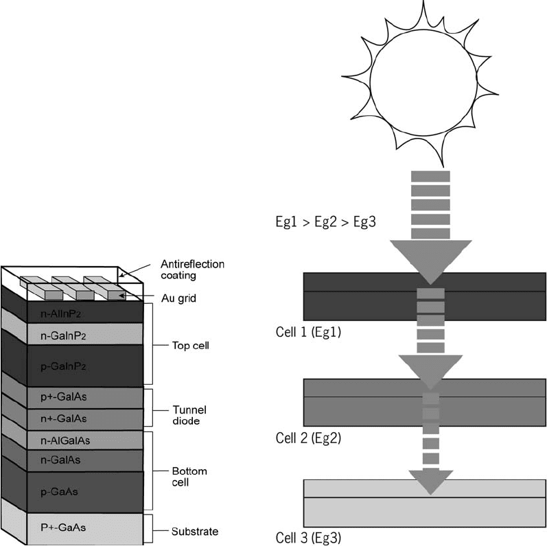
stack of individual single-junction cells in des-
cending order of bandgap (e.g. see Figure A.6).
The top cell captures the high-energy photons
and passes the rest of the photons on, to be
absorbed by lower-bandgap cells.
A multijunction cell can be made in two
different ways. In the mechanical stack approach,
two individual solar cells are made indepen-
dently, one with a high bandgap and one
with a lower bandgap. The two cells are then
mechanically stacked, one on top of the other.
In the monolithic approach, one complete solar
cell is made first, then the layers for the second
cell are grown or deposited directly on the first.
This multijunction device has a top cell of gallium
indium phosphide, then a “tunnel junction” to
allow the flow of electrons between the cells,
and a bottom cell of gallium arsenide (GaAs).
Current research in multijunction cells focu-
ses on GaAs as one (or all) of the component
cells. These cells have efficiencies of more than
35% under concentrated sunlight, which is high
for PV devices. Other materials studied for
multijunction devices are amorphous silicon
and copper indium diselenide.
Photovoltaic generator All PV strings of a PV
power supply system, which are electrically
connected.
Photovoltaic module The PV module is made
up of single solar cells, which are interconnected
Figure A.5 A multijunction photovoltaic device–
mechanical stack approach
Source: US Department of Energy
Figure A.6 A multijunction photovoltaic device–
monolithic approach
Source: US Department of Energy
280 Photovoltaic generator
to form larger units to generate electricity or
voltage for different uses. Cells connected in
series have a higher voltage, while those con-
nected in parallel produce more electric cur-
rent. The interconnected solar cells are usually
embedded in transparent ethyl vinyl acetate, fitted
with an aluminum or stainless steel frame and
covered with transparent glass on the front side.
A junction box on the underside of the module
is used to allow for connecting the module
circuit conductors to external conductors.
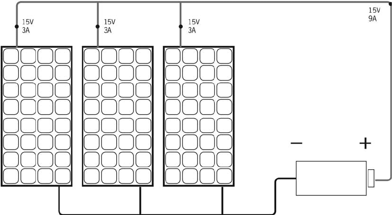
A system of PV modules functions as an
electricity-producing unit. The modules can be
connected in series, in parallel, or both to increase
output voltage or current. This also increases
the output power. The electrical current increa-
ses when modules are connected in parallel.
Figure A.7 shows three modules that produce
15 volts and 3 amps each, connected in parallel.
They will produce 15 volts and 9 amps.
If the system includes a battery storage
system, a reverse flow of current from the bat-
teries through the PV array can occur at night.
This flow will drain power from the batteries. A
diode is used to stop this reverse current flow.
Diodes are electrical devices that allow current
to flow only in one direction. Diodes create a
voltage drop, so some systems use a controller
that opens the circuit instead of using a block-
ing diode. If the same three modules are con-
nected in series, the output voltage will be 45
volts, and the current will be 3 amps.
If one module in a series string fails, it pro-
vides so much resistance that other modules in
the string may not be able to operate either. A
bypass path around the disabled module will
eliminate this problem. The bypass diode allows
the current from the other modules to flow
through in the “right” direction. Many modules
are supplied with a bypass diode at their elec-
trical terminals. Larger modules may have three
groups of cells, each with its own bypass diode.
Isolation diodes are used to prevent the power
from the rest of an array from flowing through a
damaged series string of modules. They operate
like a blocking diode. They are normally required
Figure A.7 Three modules connected in parallel
Source: US Department of Energy
Photovoltaic module 281
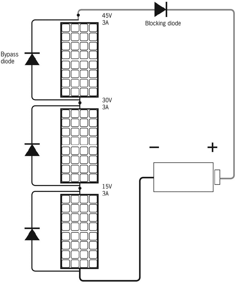
Figure A.8 Three modules connected in series with a blocking diode and bypass diodes
Source: US Department of Energy/Polar Power
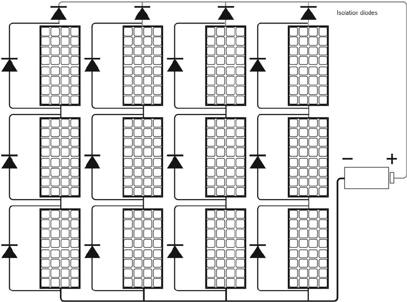
when the array produces 48 volts or more. If
isolation diodes are used on every series string,
a blocking diode normally is not required.
Modules should be installed within 200° of
true south. In areas with morning fog, the array
can be oriented up to 200° toward the west
to compensate. Similarly, arrays in areas with
frequent afternoon storms can be oriented
toward the east. If the array is in the Southern
Hemisphere, the array must face true south.
Small portable arrays are usually pointed at the
Sun, and moved hourly to track the Sun’s path
across the sky. See also main entry:
Photovoltaic
module
Photovoltaic system A PV or solar cell is the
basic building block of a PV (or solar electric)
system. An individual PV cell is usually quite
small, producing about 1 or 2 watts of power.
To boost the power output of PV cells, they
are connected together to form larger units or
modules. Modules, in turn, can be connected
to form even larger units, called arrays, which
can be interconnected to produce more
power. By themselves, modules or arrays do not
represent an entire PV system. Structures are
needed to point them toward the Sun, and
components are needed to convert the DC
electricity produced by modules and “condi-
tion” that electricity to AC electricity. There may
also be a need to store some electricity, usually
in batteries, for later use. All these items are
referred to as the “balance of system” (BOS)
components.
Figure A.9 Twelve modules in parallel-series array with bypass diodes and isolation diodes
Source: US Department of Energy/Polar Power
Photovoltaic system 283
Combining modules with the BOS compo-
nents creates an entire PV system. This system is
usually designed to meet a particular energy
demand, such as powering a water pump, or
the appliances and lights in a home, or, if the
PV system is large enough, all the electrical
requirements of a whole community.
A complete set of components for converting
sunlight into electricity by the PV process,
including the array and balance of system
components, is composed of three subsystems.
Power generation—includes a subsystem of
PV devices (cells, modules, arrays) and converts
sunlight to DC electricity.
Power use—requires a subsystem consisting
mainly of the load, which is the application
of the PV electricity.
Balance of system —between these two, a
third subsystem that enables the PV-generated
electricity to be applied properly to the
load.
See also main entry:
Photovoltaic system:
Figure 57
PV systems can be classified into two general
categories: flat-plate systems or concentrator
systems.
Flat-plate PV system The most common array
design uses flat-plate PV modules or panels,
which can be either fixed in place or allowed to
track the movement of the Sun. They respond to
sunlight that is either direct or diffuse. Even in
clear skies, the diffuse component of sunlight
accounts for between 10 and 20% of the total
solar radiation on a horizontal surface. On
partly sunny days, up to 50% of that radiation is
diffuse; on cloudy days, 100% of the radiation
is diffuse.
Figure A.10 Flat-plate PV system
Source: US Department of Energy
284 Flat-plate PV system
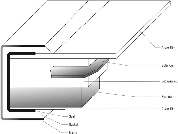
A typical flat-plate module design uses a
substrate of metal, glass, or plastic to provide
structural support in the back; an encapsulant
material to protect the cells; and a transparent
cover of plastic or glass. The simplest PV
array consists of flat-plate PV panels in a fixed
position. The advantages of fixed arrays are
that they lack moving parts, there is virtually
no need for extra equipment, and they are
relatively lightweight. These features make them
suitable for many locations, including most
residential roofs. Because the panels are fixed
in place, their orientation to the Sun is
usually at an angle that is less than optimal.
Therefore less energy per unit area of array is
collected, compared with that from a tracking
array. However, this drawback must be
balanced against the higher cost of the tracking
system.
Concentrator PV system This system uses
optical concentrators to focus direct sunlight
onto solar cells for conversion to electricity. It
includes concentrator modules, support and
tracking structures, a power-processing center,
and land. The PV concentrator module
components include solar cells, electrical iso-
lating and thermally conducting housing for
mounting and interconnecting the cells, and
optical concentrators. The solar cells are pre-
dominantly silicon, but gallium arsenide (GaAs)
solar cells are being developed for high con-
version efficiencies. Current concentrator types
include the Fresnel lens (both linear and point
focus), the Graetzel cell, the reflecting parabolic
trough, and other innovative optic devices.
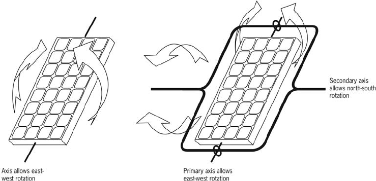
Photovoltaic tracking array Array that tracks
or follows the Sun across the sky. Tracking
arrays perform best in areas with clear climates.
The ability to follow the Sun produces sig-
nificantly greater amounts of energy when the
Sun’s energy is predominantly direct. Direct
radiation comes straight from the Sun, rather
than the entire sky. Tracking arrays can follow
the Sun in one axis or in two.
One-axis trackers normally follow the Sun
from east to west throughout the day. The angle
between the modules and the ground does not
change. The modules face in the compass
direction of the Sun, but may not point exactly
up at the Sun at all times.
Figure A.11 One-axis and two-axis tracking arrays
Source: US Department of Energy/Polar Power
Photovoltaic tracking array 285
Two-axis trackers change both their east–
west direction and the angle from the ground
during the day. The modules face straight at the
Sun all through the day. Two-axis trackers are
considerably more complicated than one-axis
types.
Various tracking systems can be used. The
first uses a simple motor, gear, and chain
system to move the array. The system is
designed to point the modules mechanically in
the direction of the Sun. No sensors or devices
actually confirm that the modules are facing the
right way.
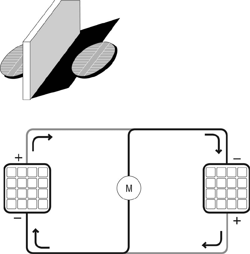
The second method uses PV cells as sensors
to orient the larger modules in the array. This
can be done by placing a cell on each side of a
small divider, and mounting the package so it is
facing the same way as the modules.
An electronic device constantly compares the
small current flow from both cells. If one is shaded,
the device triggers a motor to move the array
until both cells are exposed to equal amounts of
sunlight. At night, or during cloudy weather, the
output of both sensor cells is equally low, so no
adjustments are made. When the Sun comes
back up in the morning, the array will move back
to the east to follow the Sun again.
Although the methods of tracking with motors
are quite accurate, there is a “parasitic” power
consumption. The motors take up some of the
energy the PV system produces. A method that
has no parasitic consumption uses two small PV
modules to power a reversible-gear motor
directly. If both modules are in equal sunlight,
Figure A.12 Photovoltaic cell used as solar sensor
Source: US Department of Energy/Polar Power
Figure A.13 Current flow with both modules in equal sunlight
Source: US Department of Energy/Polar Power
286 Photovoltaic tracking array
current flows through the modules and none
flows through the motor.
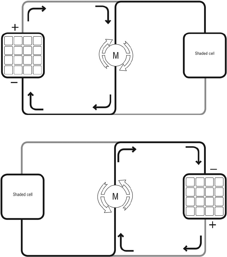
If the right module is shaded, it acts as a resistor.
Now the current will flow through the motor,
turning it in one direction.
If the other module is shaded, the current from
the right module flows in the opposite direction.
The motor will turn in the opposite direction
as well.
The motor must be able to turn in both directions.
Figure A.14 Current flow in one module (shaded)
Source: US Department of Energy/Polar Power
Figure A.15 Current flow with the other module shaded
Source: US Department of Energy/Polar Power
Photovoltaic tracking array 287
Openmirrors.com