Alkauskas A., Deak P., Neugebauer J., Pasquarello A., Van de Walle Ch.G. (Eds.) Advanced Calculations for Defects in Materials: Electronic Structure Methods
Подождите немного. Документ загружается.

1.07 eV compared to 1.19 eV experimentally. For GaAs, the band gap increases from
0.87 eV in GGA to 1.47 eV in SX. For insulators, SiO
2
, the gap improves from 6.0 eV
in GGA to 8.74 eV in SX, very close to the 9.0 eV experimental value. For wide gap
insulators such as LiF, the gap is 13.27 eV in SX, 9.24eV in PBE, compared to 13.7 eV
experimentally. It has been used before on HfO
2
and the multiferroic BiFeO
3
[30–32].
The improvement is most significant for the transparent conducting oxides such
as ZnO, In
2
O
3
and SnO
2
. These band structures are characterized by a single, broad
conduction band minimum at C. The minimum gap of SnO
2
is 0.9 eV in GGA, and
this becomes 3.66 eV in SX, compared to 3.6 eV found experimentally. The reason is
that direct gap at C is unrepresentative of the averaged gap. The average gap opens up
by the typical 20%, but this translates into a very large fractional change at C.
5.3.1
Band Structure of ZnO
ZnO is an important semiconductor, which is widely used as a phosphor, for
transparent electrodes in solar cells, and for ultraviolet light emission, spintronics,
nanowires and for its high electron mobility [33–39]. It can be easily doped n-type but
it is difficult to dope p-type [35]. This has been attributed to the nature of its intrinsic
defects which cause a self-compensation of free carriers [40] and also to that common
acceptors are deep [41]. It is therefore important to understand the energetics of its
intrinsic defects.
There have been numerous first-principles studies of the bulk electronic structure
of ZnO [13, 42–48] and its defect energies [49–63].The LDA þ U method has been
used to improve the GGA band structure, by shifting the Zn 3d band downwards [13].
The SIC method has been used to find the band structure of ZnO [44]. Various
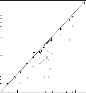
105210.5
0.5
1
2
5
10
Experimental band gap (eV)
SX band gap (eV)
Ge
CdO
Si
GaAs
SiO2
Al2O3
MgO
diamond
ZnO
ZnS
ZnSe
CdS
CdSeAlP
AlSb
SrTiO3
GGA
HfO2
In2O3
LiF
GaN
Figure 5.1 (online colour at: www.pss-b.com) GGA and SX band gaps, compared to experiment
values. Closed Circles refer to the SX band gap, open circles refer to the GGA band gap.
5.3 Bulk Band Structures and Defects
j
83

types of GW methods have been used for ZnO [45–47]. The HSE hybrid has been
used [47, 48, 52, 56, 61].
Defect calculations generally find that the O vacancy is the defect with lowest
formation energy but it is deep, while the Zn interstitial is shallow but has higher
formation energy. Nevertheless, there is a lack of consistency between the various
results. This arise partly because of the band gap error of LDA and also sometimes
because charge state corrections were not correctly included.
Patterson [54] used the B3LYP functional and localized orbitals to calculate the
defect eigenvalues, but he did not calculate the defect formation energies from the
total energies. Oba et al. [52] used the HSE functional to provide a complete set of
defect formation energies, and tested the corrections for supercell size. Superficially,
this is a well-defined calculation. However, it was necessary to increase the HF mixing
parameter a from a ¼0.25 to 0.375 in order to empirically fit the experimental gap.
Agoston et al. [56] produced a valuable comparison of GGA and HSE results for
O vacancies for all three conducting oxides.
Recently, we applied the SX method to the intrinsic defects of ZnO [61]. For our SX
calculations, k
s
is determined from the valence electron density, and for those
elements like Zn with shallow filled d states, it is for s, p electrons only. The
k
TF
¼2.27 A
1
for ZnO. A plane-wave cut-off energy of 800 eV is used, which
converges total energy differences to better that 1 meV/atom. Integrations over the
Brillouin zone are performed using the k-point sampling method of Monkhorst and
Pack with a grid that converges the energies of the bulk unit cell to a similar accuracy.
Geometry optimizations are performed self-consistently using a minimization
scheme and the Hellmann–Feynman forces, and are converged when forces are
below 0.04 eV/A
.
Table 5.2 shows the converged lattice parameters of ZnO, which are within 0.5% of
experiment, whereas GGA (PBE) values are 1% too large. The free energy of ZnO per
formula unit is found to be only 0.3 eV less than experiment, a 60% improvement
over the PBE result.
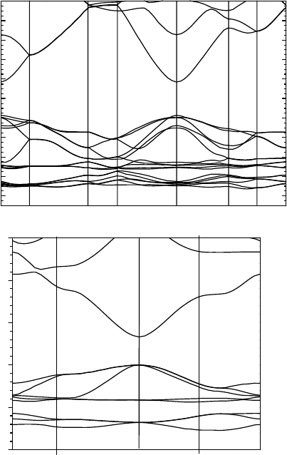
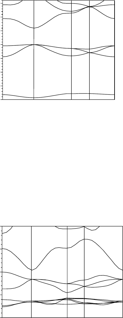
Figure 5.2 shows the calculated band structure of bulk ZnO in the wurtzite and
zincblende structure. The minimum gap is calculated to be 3.41 eV, and is very close
to the 3.44 eV found experimentally [35]. Our value is much closer to experiment than
HSE with the normal a parameter (2.87 eV) [48], or even with the expensive GW [45]
which gets 2.7 eV.
Table 5.2 Bulk properties of wurzite ZnO, calculated compared to experiment.
GGA SX exp
a (A
) 3.286 3.267 3.2495
c (A
) 5.299 5.245 5.2069
free energy (eV) 2.82 3.31 3.63
direct gap (eV) 0.9 3.41 3.44
Zn 3d (eV) 4.8 7.0 7.3
84
j
5 Calculation of Semiconductor Band Structures and Defects by the Screened Exchange
Part of the LDA band gap error in ZnO arises from the Zn 3d (t
2g
) levels lying too
high, and their upwards repulsion of the C
15
valence band maximum states. In SX,
the Zn 3d states now lie at 7.0 below the VB maximum, very close to where they are
found experimentally by angle-resolved photoemission [64, 65].
5.3.2
Defects of ZnO
The defect calculations are carried out using a 120 atom supercell, whose size is fixed
at that of the defect-free cell, and the defect created. The internal geometry is relaxed
within SX, using a single special k-point of (1/4, 1/4, 1/3) for Brillouin zone
integrations, which converges the quantities faster than the C point with respect
to supercell size [66].
-8
-6
-4
-2
0
2
4
6
8
10
12
Energy (eV)
Γ Α Η Κ Γ
MLH
w-ZnO sX
-10
-5
0
5
10
15
Energy (eV)
W L Γ X W
ZnO cubic
Figure 5.2 The band structure of ZnO in the wurtzite and zincblende structures evaluated using the
SX functional.
5.3 Bulk Band Structures and Defects
j
85
The to tal energy (E
q
) is calculated for the defect cell of charge q,fortheperfect
cell (E
H
)ofchargeq, and for a perfect cell of charge 0. This allows us to calculate
the defect formation energy, H
q
, as a function of the relative Fermi energy (DE
F
)
from the valence band edge E
V
and the relative chemical potential (Dm)of
element a [60],
H
q
ðE
F
; mÞ¼½E
q
E
H
þqðE
V
þDE
F
Þþ
X
a
n
a
m
0
a
þDm
a
;
where q(E
V
þ DE
F
) is the change in energy when charge q is added to the system at
the Fermi level and n
a
is the number of atoms of species a.Essentially,thisisthe
shift in the average electrostatic potential due to the charge of the system with
respect to the uncharged system. The corrections for the background charge, band
filling, etc., are included as described in Ref. [58]. The oxygen chemical potential
(m
0
)isreferredtothatoftheO
2
molecule, taken as zero, which is the O-rich limit.
The O-poor limit corresponds to the Zn/ZnO equilibrium and is m(O) ¼3.31 eV
(the heat of formation of ZnO).
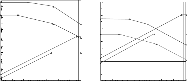
Figure 5.3a and b shows the calculated formation energies of the four intrinsic
defects of ZnO in the O-rich and O-poor limits. We see that the O vacancy (V
O
) has the
lowest formation energy over a wide range of E
F
, lower than the Zn interstitial. V
O
is
a deep defect and it has a transition state between its neutral and doubly positive states
E(0/2 þ) at 2.20 eV. The þ1 state is never stable, so the O vacancy has a negative
effective correlation energy (U), as found by others. We find U ¼2.0 eV, the energy
difference between the metastable 0/ þ and þ/2 þ transitions in Figure 5.4. The
negative U arises because of the strong lattice relaxation with changing charge state,
with the Zn-vacancy distance changing from 1.84 A
for V
0
, to 2.16 A
for V
þ
to 2.46 A
for V
2 þ
, compared to a bulk Zn–O distance of 1.95 A.
3.532.521.510.50
-4
-3
-2
-1
0
1
2
3
4
5
6
7
8
9
10
a)
Fermi ener
g
y (eV)
Formation energy (eV)
V
O
V
Zn
I
Zn
I
O
Ec
Ev
O poor
2+
0
2-
-
0
b)
3.532.521.510.50
-3
-2
-1
0
1
2
3
4
5
6
7
8
9
Fermi energy (eV)
Formation energy (eV)
V
O
V
Zn
I
Zn
I
O
Ec
Ev
O rich
2+
0
0
-
2-
Figure 5.3 (online colour at: www.pss-b.com) The formation energies of native defects in
ZnO evaluated using the SX functional under (a) oxygen poor and (b) oxygen rich conditions.
The gradients of the lines give the charge state of the defect.
86
j
5 Calculation of Semiconductor Band Structures and Defects by the Screened Exchange
These relaxations are seen in Figure 5.5a–c. Note that the relaxed structures found
by SX are similar to those found by GGA, so in fact in this case, we could have used SX
post-processing on GGA structures to find the defect formation energies.
We find that the Zn interstitial I
Zn
is a shallow defect, with a slightly higher
formation energy than V
O
. Its transition state (0/2 þ) lies at 3.32 eV, essentially at the
conduction band edge, consistent with experiment [37], and it has a U ¼0eV.
However, its neutral state has a large formation energy in O
poor conditions.
The other two intrinsic defects I
O
and V
Zn
are more stable in O-rich conditions
(compared to V
O
and I
Zn
), and have higher formation energies. They are both deep
defects, and show two charge states in the gap, corresponding to positive U behaviour.
The I
O
forms the usual dumb-bell structure of O interstitials in its 0 and charge
states, while the I
Zn
sits in the octahedral site as seen by others [50].
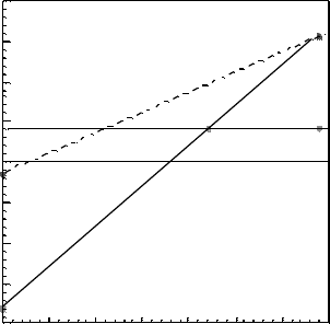
Figure 5.6 compares our formation energies of the O vacancy to those calculated by
others. The calculated formation energy of V
0
of þ0.85 eV in SX is similar to that
found by Lany and Zunger [59], slightly less than the 1.0 eV found by Oba et al. [52],
and similar to that found by Agoston et al. [56]. However, it is much less than the
formation energy given by Janotti and van de Walle [50]. The þ0.85 eV formation
energy would correspond to a frozen-in vacancy concentration of 10
19
cm
3
at 700
C,
which is consistent with the concentration found experimentally [67, 68]. However,
being deep, it is not a source of free electrons. The large formation energy of neutral
Zn interstitial means that this cannot be the source of free electrons in ZnO, as its
concentration would be too low [69]. This means that in the absence of hydrogen, the
source of free electrons must be a donor complex.
Our (0/2 þ) transition energy of 2.20 eV above the valence band top is the same as
that found by Janotti and van de Walle [50, 51], by Oba et al. [52], and Agoston et al. [56],
but higher than found by Lany in corrected GGA [59]. The metastable (0/ þ)
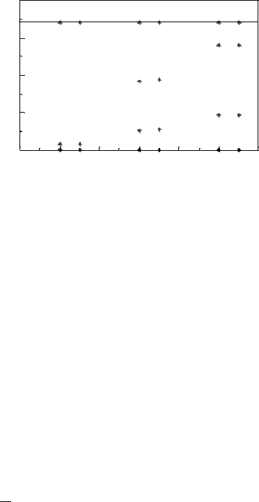
3.532.521.510.50
-4
-3
-2
-1
0
1
2
3
4
Fermi ener
g
y (eV)
Formation energy (eV)
0
+1
+2
O poor
Figure 5.4 (online colour at: www.pss-b.com) The formation energy of the neutral, þ1 and þ2
charge states of the oxygen vacancy in ZnO under oxygen poor conditions.
5.3 Bulk Band Structures and Defects
j
87
transition lies at 0.9 eV and this is consistent if the ODMR transition observed by
Vlasenko and Watkins [70] is from valence band to the defect level. Thus, overall there
is now a reasonable convergence in formation energies and transition energies
between some of the calculations.
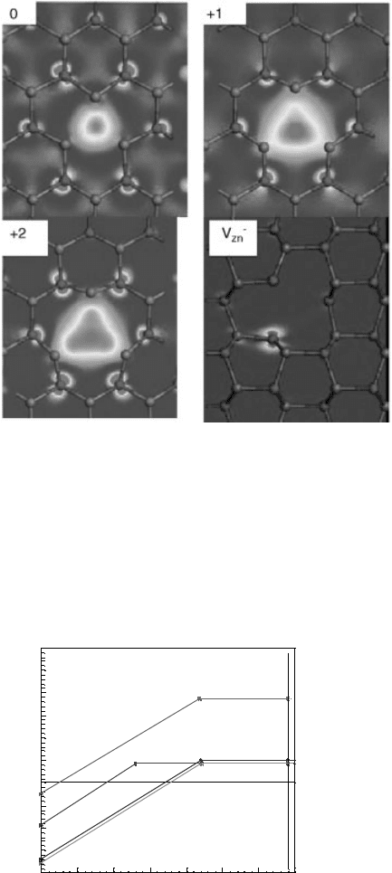
Figure 5.5 (online colour at: www.pss-b.com)
In (a), (b) and (c), the electronic density of the
defect state found in the band gap of ZnO is
shown for the oxygen vacancy for the neutral,
þ1 and þ2 charge states, respectively. In (d),
the defect state of the Zn vacancy is shown and
is found to be a p-like state located on only one of
the adjacent oxygen atoms.
3.532.521.510.50
-4
-3
-2
-1
0
1
2
3
4
5
6
Fermi energy (eV)
Formation energy (eV)
LZ
JV
SX
Oba
Ev
Ec
O poor
V
O
+2
0
Figure 5.6 (online colour at: www.pss-b.com) The oxygen vacancy formation energy under oxygen
poor conditions as a function of Fermi energy is shown for the present (SX) and other studies. Janotti
and van de Walle (JV) [49], Lany and Zunger (LZ) [58], and Oba et al. [52].
88
j
5 Calculation of Semiconductor Band Structures and Defects by the Screened Exchange
It is interesting that for the oxygen vacancy, the SX and GGA relaxed atomic
positions and wave functions are similar.
Figure 5.7 shows our calculated eigenvalues of the oxygen vacancy. We see that
theeigenvalueoftheneutralV
O
lies at þ0.16 eVabove the VB top. In GGA, it lies in
the lower gap . T his is why V
O
is able to display three charges even in GGA
calculations despite the severe under-estimate of the gap. However, it d oes show
that the calculated eigenvalues of V
O
have little relationship to the transition
energies in ZnO, due to the strong latt ice relaxations. Hence the result of the
B3LYP calculation of Patterson [54] is not particularly relevant, as it only gives
transition energies.
Finally, the LDA is known to under-estimate the localization of hole states. For
example, the trapped hole state of Al
Si
in SiO
2
(smoky quartz) is well known to be
trapped on a single oxygen, but LDA finds it localized on all four neighbouring
oxygens [71]. There are other recent examples [71, 72]. Figure 5.5d shows the
calculated SX charge density of the single trapped hole state of the Zn vacancy
V
Zn
.Wefind it to be localized on one oxygen neighbour in SX, not four. In this case,
the charge density in SX differs considerably from that of GGA. This is consistent
with its spin resonance signature [73, 74]. Even LDA þ U cannot localize it on one
oxygen [51]. On the other hand, the wave functions of the three states of V
O
are
localized over all four Zn neighbours, consistent with a simple symmetric vacancy
(Figure 5.5a–c). The localization is driven by distortion. Thus, in this case, the SX and
GGA geometries are different, we could not have found defect formation energies by
post-processing GGA geometries in SX.
5.3.3
Band Structure of MgO
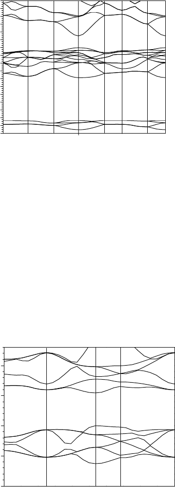
Figure 5.8 shows the SX band structure of the clasical metal oxide MgO. Its calculated
band gap is 7.7 eV, which is close to the experimental value of 7.8 eV. The valence band
is formed of O 2p states and the conduction band is formed of Mg 3s states.
0
1
2
3
4
Energy (eV)
V
0
V
+
V
2+
E
c
ZnO : O vacancy (sX)
Figure 5.7 (online colour at: www.pss-b.com) The energy eigenvalues of the oxygen vacancy defect
states lying in the band gap for SX.
5.3 Bulk Band Structures and Defects
j
89
5.3.4
Band Structures of SnO
2
and CdO
The three transparent conducting oxides ZnO, CdO and SnO
2
are good tests of band
structure methods. ZnO has been treated already. CdO fails badly in GGA, where it is
found to have a negative indirect band gap. In SX, the band gap is now positive, and
0.9 eV. This is close to the experimental value (Table 5.1). Note that CdO has an
indirect gap from L to C, due to the effect of Cd d states on the upper valence band. Its
conduction band is the standard free-electron like band, formed from Cd s states
(Figure 5.9).
-20
-15
-10
-5
0
5
10
15
Energy (eV)
L
Γ X W
Γ
MgO sX
Figure 5.8 SX band structure of MgO in the rock salt structure.
-10
-5
0
5
10
Energy (eV)
L Γ X W
Γ
CdO sX
Figure 5.9 Calculated SX band structure of rock salt CdO. Note the real gap.
90
j
5 Calculation of Semiconductor Band Structures and Defects by the Screened Exchange
SnO
2
has a simpler band structure, with a 3.6 eV direct-forbidden gap. However, in
GGA the gap is typically only 0.9 eV. Figure 5.10 shows the calculated SX band
structure, where the calculated gap is 3.6 eV, the experimental value. The band gaps
between O 2p valence states and Sn s conduction band states.
5.3.5
Band Structure and Defects of HfO
2
We have carrie d out a SX calculations on various other oxides. HfO
2
is an important
oxideinmicroelectronicsasitisnowusedasthegateoxideinmodernFETs.Itis
a closed shell t ransition metal oxide wit h a high dielectric constant. Figure 5.11
shows the band structure of cubic HfO
2
(fluorite structure) calculated by the SX
functional [30]. The calculated band gap is slightly indirect and is 5.6 eV, which is
-10
-5
0
5
10
Energy (eV)
L Γ X W
Γ
c-HfO
2
sX
Figure 5.11 Band structure of cubic HfO
2
calculated by the SX method. The calculated band gap is
5.6 eV, compared to 5.8 eV experimentally.
-22
-20
-18
-16
-14
-12
-10
-8
-6
-4
-2
0
2
4
6
8
10
12
Energy (eV)
Z A M Γ Z R X Γ
SnO
2
sX
Figure 5.10 Calculated SX band structure of SnO
2
in the rutile structure.
5.3 Bulk Band Structures and Defects
j
91
close to the experimental value of about 5.8 eV, whereas it is about 3.4–3.7 eV in
LDA or GGA.
Defects are an important consideration in such oxides, as they lead to charge
trapping, and an instability in the gate threshold voltage. The principle defect is now
known to be the oxygen vacancy. From GGA calculations, it was unclear which defect
was predominant, because GGA placed the vacancy levels either too low in the gap, or
too high in the gap [75, 76], depending on which correction scheme was applied to the
energy levels for the band gap error. SX played a critical role in resolving this question,
as it was the first calculation of the oxygen vacancy levels which placed the energy
levels correctly [30], and close to the experimental values observed by charge injection
and optical absorption [77–81]. It was then realized that the oxygen vacancy was
likely to be the main defect, as this is consistent with its behaviour in similar oxides
such as ZrO
2
.
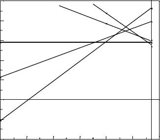
Figure 5.12 shows the calculated SX formation energy of the oxygen vacancy versus
the Fermi energy. The local structure was relaxed by SX. The lines represent the
different charge states of the vacancy, and the transition states are where lines cross.
Figure 5.12 shows that the O vacancy is a negative U defect for both the 2 and þ1
states. The calculated values are similar to those found by Gavartin et al. [82] and
Broqvist and Pasquarello. [83] using the B3LYP and PBEh methods.
5.3.6
BiFeO
3
BiFeO
3
is the architypal multiferroic oxide, which shows both ferroelectric and
antiferromagnetic properties. The interest arises from the possible electric field
control of magnetic properties and vice versa. It is highly studied since it was made in
thin film form on Si [84]. It has the R3c structure in its ferroelectric phase, which is
6543210
-4
-2
0
2
4
6
8
10
Fermi Energy (eV)
Formation Energy (eV)
+2
+1
-1
-2
0
Figure 5.12 Defect formation energy versus Fermi energy for the oxygen vacancy in HfO
2
, for an
oxygen chemical potential of the O
2
molecule.
92
j
5 Calculation of Semiconductor Band Structures and Defects by the Screened Exchange