Alkauskas A., Deak P., Neugebauer J., Pasquarello A., Van de Walle Ch.G. (Eds.) Advanced Calculations for Defects in Materials: Electronic Structure Methods
Подождите немного. Документ загружается.

and the accuracy of the calculated defect levels, in our opinion, still needs experi-
mental verification.
13.3
Symmetry and Occupation of Defect Levels
It is often very useful to know the symmetry and character of the single-particle defect
level before we start the calculation, because it can help us identify the defect level and
because defects with different symmetry and character will behave differently.
Moreover, to modify defect states or correct the band gap error, it is also important
to know the symmetry of the state. For example, although both anion vacancy and
cation interstitial have the same a
1
defect levels in II–VI semiconductors [23], anion
vacancy has the a
v
1
character derived from the valence band or cation dangling bond
states, whereas cation interstitial has instead the a
c
1
character derived from the
conduction band. Thus, the energy level of the cation interstitial is expected to follow
closely with the CBM, whereas the energy level of anion vacancy state will not.
For simple extrinsic impurities, one can predict in principle whether a dopant is
a donor with a single-particle energy level close to the CBM or an acceptor with
a single-particle energy level close to the VBM by simply counting the number of the
valence electrons of the dopants and the host elements. For example, in CdTe, one can
expect that group-I elements substituting on the Cd site, X
I
Cd
create acceptors,
whereas group-VII elements substituting on the Te site, Y
VII
Te
creates donors.
Generally speaking, to produce a shallow acceptor, it is advantageous to use a more
electronegative dopant, whereas to produce a shallow donor, it is advantageous to use
a less electronegative dopant.
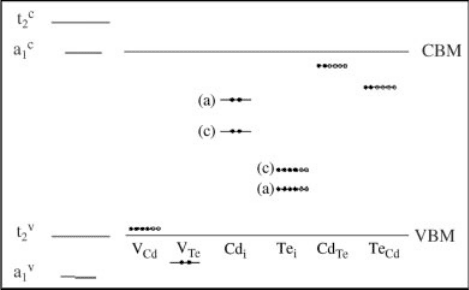
For intrinsic defects, the situation is more complicated. Figure 13.2 shows the
single-particle energy levels of tetrahedrally coordinated charge-neutral defects in
CdTe [23]. Generally speaking, when a high-valence atom is replaced by a low-valence
Figure 13.2 (online colour at: www.pss-b.com) Single-particle defect levels for the tetrahedrally
coordinated neutral intrinsic defects in CdTe. The solid (open) dots indicate the state is occupied
(unoccupied).
13.3 Symmetry and Occupation of Defect Levels
j
217
atom (e.g., Cd
Te
) or by a vacancy V
Cd
and V
Te
, defect states are created from the host
valence (v) band states that move upward in energy. The defect states consist of a low-
lying singlet a
v
1
state and a high-lying threefold-degenerate t
v
2
state. Depending on the
potential, both a
v
1
and t
v
2
can be above the VBM. These states are occupied by the
nominal valence electrons of the defect plus the valence electrons contributed
from the neighboring atoms (e.g., in CdTe, six electrons if the defect is surrounded
by four Te atoms or two electrons if it is surrounded by four Cd atoms). For example,
for charge-neutral V
Cd
, the defect center has a total of 0 þ 6 ¼6 electrons. Two of
them will occupy the a
v
1
state and the remaining four will occupy the t
v
2
states just
above the VBM, so V
Cd
is an acceptor. On the other hand, if a low-valence atom is
replaced by a high-valence atom (e.g., Te
Cd
), or if a dopant goes to an interstitial site
(e.g., Cd
i
and Te
i
), the a
v
1
and t
v
2
are pulled down and will remain inside the valence
band. Instead, the defect states a
c
1
and t
c
2
are created from the host conduction band
states that move down in energy. Depending on the potential, both the a
c
1
and t
c
2
states
can be in the gap. For example, for charge-neutral Te
Cd
,6þ 6 ¼12 electrons are
associated with this defect center. Eight of them will occupy the bonding a
v
1
and t
v
2
states, two will occupy the a
c
1
state, and the remaining two will occupy the t
c
2
state.
Since the partially occupied t
c
2
state is close to the CBM, Te
Cd
is also a donor. For the
interstitial defect, Cd
i
has two electrons that will fully occupy the a
c
1
state and is thus
expected to be a donor. The Te
i
defect center has six electrons. Two will occupy the a
c
1
state and the remaining four will occupy the t
c
2
states. Since the partially occupied t
c
2
states are closer to the VBM, Te
i
is expected to be a deep acceptor.
13.4
Origins of Doping Difficulty and the Doping Limit Rule
In general, there are three main factors that could cause the doping limit in
a semiconductor material [10, 14, 19, 22, 23]: (i) the desirable dopants have limited
solubility; (ii) the desirable dopants have sufficient solubility, but they produce deep
levels, which are not ionized at working temperatures; and (iii) there is spontaneous
formation of compensating defects. The first factor depends highly on the selected
dopants and growth conditions. The second factor only depends on the selected
dopants. Thus, these two factors can sometimes be suppressed by carefully selecting
appropriate dopants and controlling the growth conditions. The third factor is an
intrinsic problem for semiconductors; thus, it is the most difficult problem to
overcome, especially for WBG semiconductors. This is because the formation energy
of charged compensating defects depends linearly on the position of the Fermi level,
E
F
[see Eq. (13.1)]. When a semiconductor is doped, the Fermi level shifts, which can
lead to spontaneous formation of the compensating charged defects. For example,
when a semiconductor is doped p-type, E
F
moves close to the VBM. In this case, the
formation energy of the charged donor defects decreases because they will donate
their electrons into the Fermi reservoir (Figure 13.3). In WBG semiconductors with
low VBM, the formation energy decrease of donor defects can be so large that at some
Fermi energy E
F
¼e
pin
(p)
the formation energy of certain donor defect becomes zero,
218
j
13 Overcoming Bipolar Doping Difficulty in Wide Gap Semiconductors
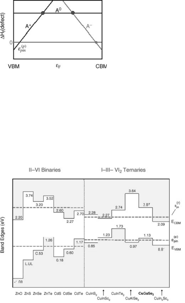
i.e., it can form spontaneously, so further shift of the Fermi energy is not possible.
Moreover, low VBM also leads to high ionization energy. Therefore, a semiconductor
with low VBM is difficult to be doped p-type. The trend for n-type doping is similar, i.e.,
a semiconductor with high CBM is difficult to be doped n-type. This doping limit rule
explains why a semiconductor with large band gap usually cannot be doped one type
or even both types under equilibrium thermodynamic growth conditions. It also
provides a general guideline about whether a material can be doped p- or n-type if we
know the band alignment between different compounds. For example, Figure 13.4
Figure 13.3 (online colour at: www.pss-b
.com) Schematic plot of the dependence of the
formation energy of charged defects on
the Fermi energy position. The p-type
pinning energy e
pin
(p)
is the Fermi
energy E
F
at which the formation energy of
donor A has zero formation energy.
Figure 13.4 (online colour at: www.pss-b.com) Band alignment and n- and p-type pinning energy
of II–VI and I–III–VI semiconductors (Ref. [10]).
13.4 Origins of Doping Difficulty and the Doping Limit Rule
j
219
shows the calculated band alignment for II–VI and I–III–VI semiconductors [10]. We
see that ZnO has very low CBM and VBM, so it can be easily doped n-type, but not
p-type. On the other hand, ZnTe with high VBM energy can be easily doped p-type,
but not n-type. For I–III–VI compounds, CuInSe
2
can be doped both p- and n-type,
but for CuGaSe
2
, n-type doping will be difficult.
Based on the above understanding, we will search for corresponding solutions to
overcome the doping limit. We will focus on the following approaches: (i) increase
defect solubility by defeating bulk defect thermodynamics using non-equilibrium
growth methods such as extending the achievable chemical potential through
molecular doping or raising the host energy using surfactant; (ii) reduce defect
ionization energy level by designing shallow dopants or dopant complexes; and (iii)
reduce defect compensation and ionization level by modifying the host band
structure near the band edges. As examples, we will discuss doping in some
representative WBG semiconductors such as n-type doping in ZnTe and diamond
and p-type doping in ZnO. The principles discussed here are general and are
applicable to other WBG semiconductors.
13.5
Approaches to Overcome the Doping Limit
13.5.1
Optimization of Chemical Potentials
13.5.1.1 Chemical Potential of Host Elements
As Eq. (13.1) indicates, the formation energy of a defect, which determines the
solubility of dopants, depends sensitively on the atomic chemical potentials of both
the host elements and the dopants [14, 19]. Thus, optimization of the growth
conditions and dopant source is critical to enhance the doping ability. So far,
computational results and analysis have focused on the dependence of formation
energies on host-element chemical potentials [27, 31]. For example, N substituting O
(N
O
) is expected to be a p-type dopant for ZnO. The formation energy of N
O
depends
on the chemical potentials of Zn, O, and N. Under thermal equilibrium growth
conditions, there are some thermodynamic limits on the achievable values of the
chemical potentials. First, to avoid precipitation of the elemental dopant and host
elements, the chemical potentials are limited by
m
Zn
mðZn metalÞ¼0; ð13:7Þ
m
O
mðO
2
gasÞ¼0; ð13:8Þ
m
N
mðN
2
gasÞ¼0: ð13:9Þ
Second, m
Zn
and m
O
are limited to the value of maintaining ZnO. Therefore,
m
Zn
þm
O
¼ DH
f
ðZnOÞ: ð13:10Þ
220
j
13 Overcoming Bipolar Doping Difficulty in Wide Gap Semiconductors
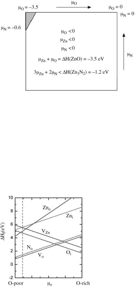
Here, DH
f
(ZnO) is the formation energy of bulk ZnO. The calculated value is
about 3.5 eV. Finally, to avoid the formation of the Zn
3
N
2
secondary phase, m
N
is also
limited by
3m
ZN
þ2m
N
DH
f
ðZn
3
N
2
Þ: ð13:11Þ
The calculated formation energy of Zn
3
N
2
is about 1.2 eV. Using the equations
above, the achievable chemical potential region is shown in Figure 13.5.
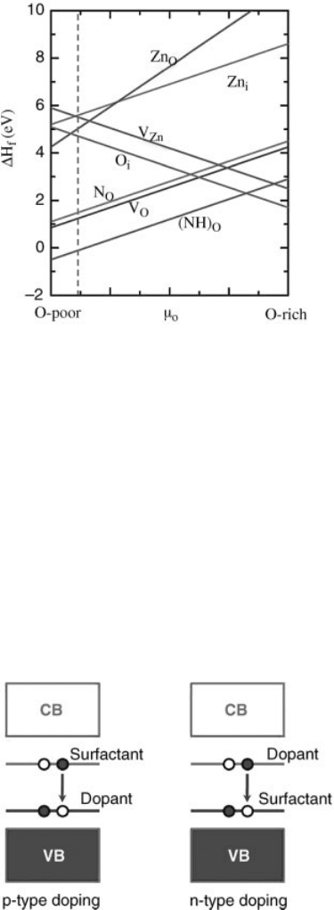
Figure 13.6 shows the calculated formation energies of charge neutral defects as
a function of the O chemical potential. Here, m
N
is derived from N
2
gas. It is seen that
the formation energy of N
O
is lower at the O-poor condition, but higher at the O-rich
Figure 13.5 The achievable chemical potential region for N doped ZnO under equilibrium growth
condition.
Figure 13.6 (online colour at: www.pss-b.com) Calculated formation energies of charge-neutral
defects as a function of O chemical potential. The dashed line indicates the growth condition at
which (left region) Zn
3
N
2
will precipitate.
13.5 Approaches to Overcome the Doping Limit
j
221

condition. Thus, to enhance the solubility of N, ZnO films should be synthesized at
O-poor conditions. It should be noted that the formation energies of other intrinsic
defects also depend on the growth conditions. At O-poor conditions, the formation
energies for acceptor-killer defects, such as Zn interstitials (Zn
i
) and O vacancies
(V
O
), are decreased. Thus, there is an intrinsic problem for enhancing the p-type
doping using N as the dopant. In Section 13.5.4, we will discuss how this dilemma
may be eliminated by selecting appropriate dopants.
The left region of the dashed line indicates the growth condition at which Zn
3
N
2
will precipitate under equilibrium growth. This indicates that the O chemical
potential should not go into this region so as to avoid the precipitation of Zn
3
N
2
.
Thus, the precipitation of a secondary phase can limit the solubility of dopants. To
overcome this, it has been shown that the precipitation of a secondary phase can be
suppressed through epitaxial growth [32]. For example, the calculated thermody-
namic solubility of N in bulk GaAs is only [N] < 10
14
cm
3
at T ¼650
C due to the
formation of a fully relaxed, secondary GaN phase. However, single-phase epitaxial
films grown at T ¼400–650
C with [N] as high as 10% have been reported. Zhang
and Wei [32] found that if coherent surface strain is considered, the formation of
the secondary GaN phase could be suppressed during epitaxial growth. As a result,
the solubility of N can be enhanced significantly. A similar approach could be used to
avoid forming Zn
3
N
2
in ZnO:N.
Avoiding the formation of secondary phase can also lead to some unexpected
consequences. For example, substituting Zn by Al for n-type doping in ZnO,
the formation energy of Al
Zn
depends on (m
Zn
m
Al
), thus one may expect that the
formation energy of Al
Zn
should reach minimum under Zn-poor condition. How-
ever, to avoid the formation of Al
2
O
3
, we need to satisfy the following condition:
2m
Al
þ3m
O
DH
f
ðAl
2
O
3
Þ: ð13:12Þ
Combine Eqs. (13.10) and (13.12), we have
ðm
Zn
m
Al
Þ
m
O
þ2DH
f
ðZnOÞDH
f
ðAl
2
O
3
Þ
2
: ð13:13Þ
That is, in the achievable chemical potential region, Al
Zn
has the lowest formation
under O-poor or Zn-rich condition.
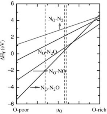
13.5.1.2 Chemical Potential of Dopant Sources
Although the dependence of doping efficiency on the host elements chemical
potential has been studied extensively, the dependence of doping efficiency on
dopant chemical potential has not attracted much attention because normally there
are no significant alternative dopant sources. However, for the case of N doping of
ZnO (or other oxides), there is a unique and unusual opportunity. There are at least
four different gases, namely N
2
, NO, NO
2
, and N
2
O that can be used as the dopant
source. If these molecules arrive intact at the growing surface, their chemical
potentials will determine the doping efficiency. We found that the N solubility can
be enhanced significantly when metastable NO or NO
2
gases are used as the dopant
sources [15]. A key feature that underlies our idea of doping with NO or NO
2
is that
222
j
13 Overcoming Bipolar Doping Difficulty in Wide Gap Semiconductors

these molecules can supply single N atoms by breaking only the weak N–O bonds,
whereas one has to break the strong N–N bonds to obtain desirable single-N defects
when N
2
and N
2
O are used. For example, when the NO, N
2
O, or NO
2
molecules arrive
intact at the growing surface, the formation energy of a charge-neutral N
O
defect is
given by
DH
f
ðN
O
; 0Þ¼EðN
O
; 0ÞEðhostÞþ2m
O
m
NO
ð13:14Þ
or
DH
f
ðN
O
; 0Þ¼EðN
O
; 0ÞEðhostÞþ1:5m
O
m
N
2
O
2
; ð13:15Þ
DH
f
ðN
O
; 0Þ¼EðN
O
; 0ÞEðhostÞþ3m
O
m
NO
2
: ð13:16Þ
Our calculated formation energy is about 0.9, 0.2, and 0.2 eV for NO, N
2
O, and NO
2
molecules, respectively. The NO and NO
2
molecules may simply be supplied as such
or they may be produced by a reaction in the gas phase. For example, NO molecules
can be created by N
2
O ,NO þ N. In this case, m
NO
¼mN
2
O – m
N
. Figure 13.7 shows
the calculated formation energy of charge-neutral N
O
for four different gases. The
difference between N
2
/N
2
O and NO/NO
2
is very clear, i.e., the use of NO/NO
2
leads
to significantly reduced formation energies for N
O
because it does not entail any
energy to break the NN bonds. The negative formation energies of N
O
at Zn-rich
conditions indicate that NO or NO
2
molecules can be incorporated spontaneously to
form N
O
defects, if these molecules are intact before they are incorporated into ZnO.
However, in practical growth conditions, to avoid the precipitation of the secondary
phases such as Zn
3
N
2
, besides satisfying
m
O
þm
N
¼ m
NO
for NO gas as dopant; ð13:17Þ
2m
O
þm
N
¼ m
NO
2
for NO
2
gas as dopant; ð13:18Þ
m
O
þ2m
N
¼ m
N
2
O
for N
2
O gas as dopant; ð13:19Þ
we also need to satisfy Eqs. (13.10) and (13.11), which set a low limit for the achievable
O chemical potential. In Figure 13.7, the left, middle, and right dashed vertical lines
indicate the low limits for O chemical potentials for N
2
O, NO, and NO
2
molecules,
respectively.
13.5.2
H-Assisted Doping
As we discussed above, the solubility of both the dopants and compensating defects
depend sensitively on the position of the Fermi level. If we can control the Fermi level
at a desirable position, then we may enhance the solubility of dopants and suppress
the formation of compensating defects. Electron or hole injection could be a method
to control the position of the Fermi level during film growth. Another popular
13.5 Approaches to Overcome the Doping Limit
j
223
approach is passivating the dopants by H atoms. For example, in Mg-doped GaN, the
introduction of H can prevent such a shift. As a result, the concentration of Mg can
be enhanced [34]. After film growth, H can be annealed out to achieve p-type
conductivity.
For N-doping in ZnO (also other oxides), the co-existence of H can, in addition to
preventing the Fermi level shift, directly passivate N dopants, forming a molecular NH
complex on O site [(NH)
O
]. The binding energy for (NH)
O
is 2.9 eV. The (NH)
O
complexes electronically mimic O atoms and cause smaller lattice distortion than N
O
.
Thus,theconcentration of (NH)
O
in ZnO can be much higherthanN
O
[14].Figure13.8
showsthe calculatedformationenergyfor (NH)
O
as a function of O chemical potential.
For comparison, the formation energies of N
O
and some hole-killer defects are also
shown. It is seen that the formation energy of (NH)
O
is lower than any other defects in
the O-poor condition. In addition, the existence of H also pins the Fermi energy level,
so the formation of compensating defects enhanced by a shifted Fermi level is also
suppressed. Therefore, p-type doping could be achieved after subsequently driving out
the hydrogen atoms from the sample by thermal annealing.
13.5.3
Surfactant Enhanced Doping
To lower the defect formation energy, which is the total energy difference between the
final doped state and the initial state, we can either increase the initial dopant energy,
as discussed in the previous section, or increase the energy of the host. Recently, we
have shown that this can be done by introducing an appropriate surfactant during
Figure 13.7 (online colour at: www.pss-b.com) Calculated formation energy of charge-neutral
N
O
withfour different dopantsources:N
2
,N
2
O, NO, and NO
2
. The left,middle, and rightdashedlines
indicate the low limits for achievable O chemical potentials for N
2
O, NO, and NO
2
molecule doping.
224
j
13 Overcoming Bipolar Doping Difficulty in Wide Gap Semiconductors
epitaxial growth [35]. The general concept for enhancing dopant solubility via
epitaxial surfactant growth is schematically described in Figure 13.9. It is known
experimentally that the surfactants in epitaxial growth float on the top surface of the
growth front. The enhancement of dopant solubility initiates in the sublayers below
the surface. For p-type doping, dopants introduce acceptor levels with holes near the
VBM of the host system. On the other hand the surfactants on the growth surface will
introduce surfactant levels. If the surfactant levels are higher in energy than the
acceptor levels and have electrons available, the surfactants will donate the electrons
to the acceptors and consequently leads to a Coulomb binding between the surfactant
and the dopant. Such charge transfer reduces the energy of the system and
consequently leads to effective reduction on the formation energy of dopant incor-
poration in the host. The formation energy reduction is large if the energy level
Figure 13.8 (online colour at: www.pss-b.com) Calculated formation energy of (NH)
O
in ZnO.
Figure 13.9 (online colour at: www.pss-b.com) Schematic plot of the mechanism of surfactant
enhanced doping during epitaxial growth.
13.5 Approaches to Overcome the Doping Limit
j
225
difference between the surfactant and acceptor levels is large. The same principle
holds for n-type doping, except that the charge transfer is from dopant level to empty
surfactant level. In this case, the positions of dopant levels are close to the CBM and
the surfactant levels must be lower in energy than the dopant levels. Thus, the key for
this concept is how to ensure that the surfactant levels are higher (lower) in energy
than the dopant levels and there are indeed electrons (holes) in the surfactant levels in
p-type (n-type) doping. We have calculated the formation energy for substitutional
Ag
Zn
in the sublayer of ZnO ð000 1
Þ surface and found that the formation energy is
lowered by 2.3 eV with S as surfactant as compared to that without surfactant.
13.5.4
Appropriate Selection of Dopants
There are two general rules for choosing an appropriate dopant to produce shallow
defect levels. First, an appropriate dopant should favor the growth conditions that will
suppress the formation of compensating defects. As we discussed in Section 13.2, the
solubility of dopants and concentration of intrinsic defects depend sensitively on the
growth conditions. It is highly desirable to have a growth condition that enhances
the dopant solubility and suppresses the formation of intrinsic compensating
defects. This may be achieved by identifying the compensating defects and choosing
suitable dopants. For example, the major defects that compensate acceptors in ZnO
are Zn
i
and V
O
. Figure 13.6 shows that to suppress the formation of these hole-killer
defects, an O-rich growth condition is preferred. Of course, this condition is not
preferred for N incorporation. However, such a growth condition is preferred for
doping at cation sites.
Second, dopants at cation sites in compound semiconductors generally produce
shallower acceptor levels than dopants at anion sites. This is because for most
cation–anion compound semiconductors, the valance bands are derived mainly from
the anion atoms. Dopant substituting at cation site would, in general, cause smaller
perturbation than dopants at anion sites on the anion-derived valance band. Thus,
theoretical studies have found that Group-I elements such as Li and Na have low
acceptor levels, whereas Group-V elements such as N, P, As, and Sb have deep
acceptor levels in ZnO [33]. The large ionization energy for Group-Vacceptors in ZnO
can be understood as follows: The acceptor level, especially the shallow acceptor level,
has a wave-function character similar to that of the VBM state, which consists mostly
of anion p, and small amounts of cation p and cation d orbitals. Therefore, to have
a shallow acceptor level, the dopant should be as electronegative as possible, that is, it
should have low p orbital energy. For example, because the atomic p orbital energy
level of N is the lowest (Figure 13.10), i.e., most electronegative, among the Group-V
elements, N has been the preferred acceptor dopant for II–VI semiconductors
because it produces the lowest acceptor levels compared to the other Group-V
dopants. However, due to the low VBM of the oxides, the level of N
O
in ZnO is
still relatively deep [19, 33] at about 0.4 eVabove the VBM, making acceptor ionization
difficult. The other Group-V elements are less electronegative than the N atom;
therefore, they have much larger ionization energy than N
O
[33]. This explains why it
226
j
13 Overcoming Bipolar Doping Difficulty in Wide Gap Semiconductors