Alkauskas A., Deak P., Neugebauer J., Pasquarello A., Van de Walle Ch.G. (Eds.) Advanced Calculations for Defects in Materials: Electronic Structure Methods
Подождите немного. Документ загружается.


exact e
1
GG
0
ðq; vÞ to the plasma frequency and the charge density [47, 48]. The final
expression for the PPM parameters are:
V
2
GG
0
ðqÞ¼v
2
p
ðq þGÞðq þG
0
Þ
jq þGj
2
nðGG
0
Þ
nð0Þ
v
GG
0
2
ðqÞ¼
V
2
GG
0
ðqÞ
d
GG
0
e
1
GG
0
ðq; v ¼ 0Þ
A
GG
0
ðqÞ¼
p
2
V
GG
0
ðqÞ
v
GG
0
ðqÞ
:
8
>
>
>
>
>
>
>
>
>
<
>
>
>
>
>
>
>
>
>
:
ð3:25Þ
Models based on Eqs. (3.22) and (3.23) have a number of undesirable features,
despite their success. For instance, for some elements with G 6¼ G
0
, the plasmon
poles v
GG
0
ðqÞ can become very small or even imaginary which is somewhat
unphysical [31].
Two more recent PPM approaches due to Von der Linden and Horsch [49] (vdLH)
and Engel and Farid [50] (EF) are expected to be more accurate. The vdLH PPM is
derived starting from the spectral decomposition of the symmetrized inverse
dielectric matrix:
e
GG
0
1
ðq; vÞ¼
jq þG
0
j
jq þGj
e
1
GG
0
ðq; vÞ; ð3:26Þ
by assuming that the frequency dependence is solely contained in the eigenvalues
(see Ref. [49]). The disadvantage of the vdLH approach is that it satisfies the f-sum rule
only for the diagonal elements. In the EF PPM, the eigenvalues and the eigenvectors
are frequency dependent, and derived from an approximation to the reducible
polarizability which is exact both in the static- and high-frequency limit. For further
details on this plasmon-pole technique, see Ref. [50].
Since the frequency convolution in Eq. (3.18) can be carried out analytically once
the plasmon-pole parameters are known, the PPM technique is an ideal tool for initial
convergence studies. It usually proves to be accurate to within 0.1–0.2 eV for states
close to the Fermi level, when compared to results obtained with a costly numerical
integration of S [27]. On the other hand, the accuracy worsens for states far from
the gap, especially for low-lying states. To analyze physical properties depending on
these, it is necessary to avoid PPM methods, and calculate the frequency dependence
of W explicitly.
A straightforward numerical evaluation of Eq. (3.18) is problematic due to the
fact that G and W both have poles infinitesimally above and below the real axis.
Therefore, a straightforward integration algorithm along the real axis would need
evaluations of the integrand precisely in the region where it is ill-behaved.
An alternative route to evaluating Eq. (3.18) traces back to the earliest GW
calculations for the homogeneous electron gas [51]. The Greens function G and
the screened Coulomb interaction W are analytic functions (except along the real
axis) and can consequently be analytically continued to the full complex plane.
The strategy is to use a deformation of the contour of integration in order to avoid
3.3 Practical Implementation of GW and Recent Developments Beyond
j
43
having to deal with quantities close to the real axis as much as possible. Instead of
evaluating the integral along the real axis, one evaluates the integral along the
imaginary axis, and then adds the residues arising from the poles enclosed in the
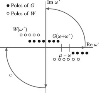
contour depicted in red in Figure 3.3.
3.3.4
The Extrapolar Method
GW calculations are computationally very demanding. Two major steps in these can
be distinguished: the calculation of the polarizability and the evaluation of matrix
elements of the self-energy. The quantities involved are not only non-local (two plane-
wave indices), but also involve summations over all states (occupied and empty).
Recently, Bruneval and Gonze [52] proposed an acceleration scheme to improve the
convergence with respect to the number of states. The main idea is to replace the
poles arising from the eigenvalues of empty high-energy states with a single (average)
pole, which carries all the spectral weight above a certain cutoff for states. Note that
the extrapolar technique was first introduced in the optimized effective potential
framework [17] and in a preconditioning scheme [53].
Both in the polarizability and in the self-energy, the expressions to be evaluated
contain a sum over wavefunctions in a numerator and energy differences in a
denominator. If we were able to factor a simple common denominator out of the sum,
it would be straightforward to eliminate the wavefunctions in the numerator, above
some cutoff band index, N
b
, by using the closure relation:
X
b>N
b
jbihbj¼1
X
bN
b
jbihbj: ð3:27Þ
Figure 3.3 (online color at: www.pss-b.com ) Schematic repre sentation of the contour of
integration in the complex v
0
planeusedtoevaluateSðvÞ. The poles of the integrand are shown
as circles. Only the poles due to Greens function t hat li e inside the path c ontribute to the final
result.
44
j
3 Electronic Properties of Interfaces and Defects from Many-body Perturbation Theory

Treating the denominator of the remainder (now dependent on all states b N
b
)is
the delicate part, which requires careful consideration.
3.3.4.1 Polarizability with a Limited Number of Empty States
Using time-reversal symmetry, the truncated expression for the independent-particle
polarizability in reciprocal and frequency space reads
P
0GG
0
ðq; vÞ¼
2
N
k
V
X
k
X
N
v
<bN
b
v N
v
M
bv
k
ðq þGÞ½M
bv
k
ðq þG
0
Þ
1
vðe
vk
e
bkq
Þig
1
vðe
bkq
e
vk
Þþig
;
ð3:28Þ
where V is the volume of the unit cell, g is a positive infinitesimal, N
v
is the number
of valence states, N
k
is the number of k-points in the Brillouin zone, and the index
k runs over the k-points of the Brillouin zone. The matrix elements:
M
bb
0
k
ðq þGÞ¼hy
bkq
je
iðq þGÞr
jy
b
0
k
i; ð3:29Þ
are the so-called oscillator strengths.
The extrapolar method proposes that the empty states above the truncation index,
N
b
, all have the same energy. In this case, the dependence with respect to index b is
removed in the denominator and one can apply the closure relation to the numerator
in order to get rid of any dependence on this index. This procedure adds a term to the
usual truncated expression for P
0
. The correction consists of two terms:
D
GG
0
ðq; vÞ¼
2
N
k
V
X
k
X
v N
v
hy
vk
je
iðG
0
GÞr
jy
vk
i
1
vðe
vk
e
P
0
Þig
1
vð
e
P
0
e
vk
Þþig
2
N
k
V
X
k
X
bN
b
vN
v
M
bv
k
ðq þGÞ½M
bv
k
ðq þG
0
Þ
1
vðe
vk
e
P
0
Þig
1
vð
e
P
0
e
vk
Þþig;
ð3:30Þ
which are now free of any dependence on states above N
b
. Instead they contain an
average energy
e
P
0
which represents the omitted part of the eigenvalue spectrum by
a mean value. The best value for
e
P
0
can be easily determined by a trial-and-error
procedure or in a more elegant manner by considering the fulfillment of the f-sum
rule for P
0
ðvÞ.
3.3 Practical Implementation of GW and Recent Developments Beyond
j
45
3.3.4.2 Self-Energy with a Limited Number of Empty States
An analogous procedure can be applied to the correlation part of the self-energy:
hy
bk
jS
c
ðe
bk
Þjy
bk
i¼
i
2pN
k
V
ð
X
b
0
N
b
X
qGG
0
½W
GG
0
ðq; v
0
Þd
GG
0
vðq þGÞ
M
bb
0
k
ðq þG Þ½M
bb
0
k
ðq þG
0
Þ
v
0
e
b
0
kq
þe
bk
ig
dv
0
;
ð3:31Þ
where g is a positive infinitesimal. The sign in front of g is plus when the state b
0
is
empty, and minus otherwise.
Unlike for the polarizability, a PPM becomes necessary for the self-energy to make
the extrapolar correction tractable. In this context, the PPM is a very good approx-
imation. The final correction reads:
D
bk
¼
1
N
k
V
X
qGG
0
V
2
GG
0
ðqÞvðq þGÞ
2v
GG
0
ðqÞ½v
GG
0
ðqÞþe
S
e
bk
ig
hy
bk
je
iðG
0
GÞr
jy
bk
i
X
b
0
N
b
M
bb
0
k
ðq þGÞ
h
M
bb
0
k
ðq þG
0
Þ
i
:
ð3:32Þ
Again, it consists of two terms that do not depend on any state above N
b
. The
introduced average energy
e
S
in the denominators can safely be taken to be equal to
the previously introduced
e
P
0
.
3.3.5
MBPT in the PAW Framework
Thanks to the excellent agreement obtained with respect to experiments, pseudopo-
tential (PP)-based methods have for several decades represented a de facto standard for
MBPT calculations. In recent years, however, results obtained with all-electron (AE)
approaches [44, 54] have revealed that a fully consistent treatment of the electronic
degrees of freedom produces GW band gaps that are systematically smaller than PP
results,thusworseningtheagreementbetween G
0
W
0
andexperiments.Thesefindings
have led to quitean intensedebatein thescientificliterature concerningthereliability of
the PP approach for MBPTcalculations (see, for instance, Refs. [55–58]).
Systems with shallow cores or localized d-orf-electrons present severe challenges
to PP GW calculations [28, 56, 58–60]. Core-valence exchange is large in these
systems, due to the large overlap of the localized d or f-states (or semicore states) with
lower-lying core states in the same atomic shell. To treat core-valence exchange
consistently it is therefore either important to let the exchange part of the GW self-
energy act on all electrons of one shell [56, 58, 59] – which can be very expensive
computationally – or to build the exchange interaction into the PP [28, 29].
The PAW formalism introduced by Bl
€
ochl in 1994 [61] presents a flexible and
efficient alternative to PPs in GW calculations. It combines the PP framework with an
46
j
3 Electronic Properties of Interfaces and Defects from Many-body Perturbation Theory
AE description and allows for results on a par with AE accuracy at considerably
reduced computational cost. The method takes advantage of several ideas and
techniques developed in the past decades both in the PP and in the AE community.
From the PP approach [62] it inherits the idea of substituting the true Kohn –Sham
wave function yðrÞwith a pseudized image y
ðrÞwhich can be efficiently expanded in
an extended basis set (e.g., plane-waves). Similar to many AE approaches, PAW
employs atomic orbitals to describe the AE wave function yðrÞ inside non-over-
lapping atom-centered spheres, thus retaining information about the correct nodal
structure of electronic orbitals.
The mapping between the true wave function, jyi, with its complete and complex
nodal structure around the nuclei, and the fictitious smooth pseudo wave functions,
jy
i,isdefined by the linear transformation: jyi¼
^
Tjy
i.
^
T is given by the identity
operator plus a sum of localized terms,
^
T
a
, only acting within the atomic spheres V
a
centered on atomic sites a:
^
T¼
^
1 þ
X
a
^
T
a
: ð3:33Þ
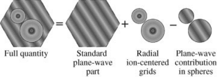
A schematic representation of the division of the unit cell employed in the PAW
method is shown in Figure 3.4.
The linear transformation within each augmentation region V
a
is defined by
specifying a set of functions, fw
a
i
g, which form a complete basis set within V
a
.
This set of functions serves as a basis set for the expansion of the true electronic wave
function in each augmentation region with coefficients c
a
i
:
jyi¼
X
i
c
a
i
jw
a
i
i in V
a
: ð3:34Þ
A possible and natural choice for the basis set fw
a
i
g are the solutions of the radial
Schr
€
odinger equation for the isolated atom. In this case the index i is a contracted
notation for the atomic position R
a
, the angular momentum quantum numbers
ðl; mÞ, and an additional index n used to label solutions with different energy.
The final expression for the linear transformation is given by [61, 63]
^
T¼
^
1 þ
X
a
X
i
ðjw
a
i
ijw
i
a
iÞhp
i
a
j: ð3:35Þ
Figure 3.4 (online color at: www.pss-b.com) Schematic representation of the division of the unit
cell employed in the PAW method.
3.3 Practical Implementation of GW and Recent Developments Beyond
j
47
where the auxiliary pseudo partial waves jw
i
a
iequal the AE counterparts jw
a
i
ibeyond
the radius r
a
c
of the PAW sphere, and are used to expand the pseudized function jy
i
inside the augmentation sphere. The atom-centered projector functions jp
i
a
i are
strictly localized inside the spheres and obey the orthogonality property:
hp
i
a
jw
j
a
i¼d
ij
: ð3:36Þ
The matrix elements of a local or semilocal operator
^
A between two AE wave
functions can be efficiently and accurately evaluated by employing the linear
transformation
^
T given in Eq. (3.35). After some algebra one obtains:
hyj
^
Ajyi¼hy
j
^
Ajy
iþ
X
ij
hy
jp
i
i½hw
i
j
^
Ajw
j
ihw
i
j
^
Ajw
j
ihp
j
jy
i:
ð3:37Þ
The first term in Eq. (3.37) has the same mathematical structure as the expression
present in the PP formalism. As it involves only the smooth part of the wave
function, it can be evaluated either in real or reciprocal space, depending on the
nature of
^
A, by changing representation through fast Fourier transform techniques.
The second term involves the onsite matrix elements of the
^
A operator between AE
and pseudo partial waves. It can be evaluated either by employing radial and angular
meshes in real space or by expanding the operator
^
A in terms of angular momenta.
Within the PAW formalism, the oscillator strengths, – i.e., the basic ingredients
required to evaluate P
0
ðvÞ, and the matrix elements of SðvÞ – can be obtained by
means of the following equation [64]:
hy
bkq
je
iðq þGÞr
jy
b
0
k
i¼hy
bkq
je
iðq þGÞr
jy
b
0
k
iþ
X
ij
hy
bkq
jp
i
ihp
j
jy
b
0
k
ie
iðq þGÞR
i
h
hw
i
je
iðq þGÞðrr
i
Þ
jw
j
ihw
i
je
iðq þGÞðrr
i
Þ
jw
j
i
i
|fflfflfflfflfflfflfflfflfflfflfflfflfflfflfflfflfflfflfflffl{zfflfflfflfflfflfflfflfflfflfflfflfflfflfflfflfflfflfflfflffl}
4p
X
lm
ðiÞ
l
Y
l
m
ð q þG
c
ÞG
lm
l
i
m
i
l
j
m
j
ð
j
l
ðjq þGjrÞðw
n
i
l
i
w
n
j
l
j
w
n
i
l
i
w
n
j
l
j
Þdr
; ð3:38Þ
where the plane wave has been expressed in terms of Bessel functions j
l
ðxÞ and real
spherical harmonics Y
l
m
ð
^
GÞvia the Rayleigh expansion. The symbol G
lm
l
i
m
i
l
j
m
j
is used to
denote the Gaunt coefficient [65], defined by:
G
lm
l
i
m
i
l
j
m
j
¼
ð
Y
l
i
m
i
Y
l
m
Y
l
j
m
j
dV: ð3:39Þ
3.4
QP Corrections to the BOs at Interfaces
In the DFT approach, the valence and conduction band offsets (VBO and CBO,
respectively) are conveniently split into two terms:
VBO ¼ DE
DFT
v
þDV; ð3:40Þ
48
j
3 Electronic Properties of Interfaces and Defects from Many-body Perturbation Theory

CBO ¼ DE
DFT
c
þDV: ð3:41Þ
The first term DE
DFT
v
(resp. DE
DFT
c
) on the right-hand side of Eq. (3.40) [resp.
Eq. (3.41)] is referred to as the band-structure contribution.Itisdefined as the
difference between the valence band maximum (VBM) (and the conduction band
minimum (CBM), respectively) relative to the average of the electrostatic potential in each
material. These are obtained from two independent standard bulk calculations on the
two interface materials. Alternatively, these can be obtained from an analysis of the
local density of states [66]. The second term DV, called the lineup of the average of the
electrostatic potential across the interface, accounts for all the intrinsic interface
effects. It is determined from a supercell calculation with a model interface.
Despite the limitations of DFT in finding accurate eigenenergies, the VBOs are
often obtained with a very good precision, in particular for semiconductors [67]. This
has opened an indirect route to computing the CBOs through the experimental band
gaps using:
CBO ¼ DE
exp
g
þVBO: ð3:42Þ
Note that this equation is equivalent to applying a scissor correction to the
conduction bands on both sides of the interface, as can be seen by inserting Eqs. (3.40)
and (3.42):
CBO ¼ DE
DFT
c
þDV þ
DE
exp
g
DE
DFT
g
; ð3:43Þ
and then comparing with Eq. (3.41).
The first QP calculation of the band-offsets (BOs) goes back to the work of Zhang
et al. [68] who were investigating the VBO at the AlAsGaAs(001) interface. They
assumed that the lineup of the potential DV is already well described within DFT,
arguing that QP corrections would not affect DV since it only depends on the long
range electrostatic potentials. The latter are well-known functions of the electronic
densities, which are given quite accurately by DFT.
Recently, the many-body effects on DV have b een explicitly investigated [69].
This was done by comparing the electronic density and the resulting
DV calculated within DFT and QSGW for a small model of the Si/SiO
2
interface
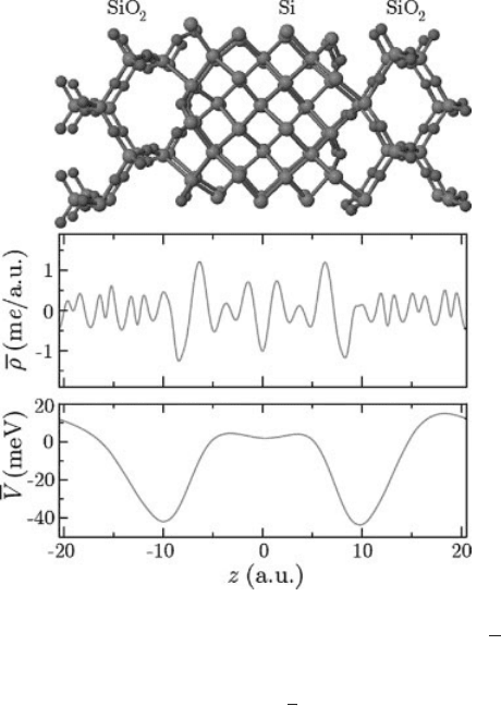
illustrated in Figure 3.5(a). It w as found that the QSGW results differ only slightly
fromDFT.Thechangeinplanaraverageoftheelectronicdensity,
r, was at most 1
me/a.u. in the interface region, as illustrated in Figure 3.5(b). This lead to a
variation in the macroscopic average of the local potential
V [Figure 3.5(c)] smaller
than 45 meV in that region. However, the net difference between the bulk
materials, which is relevant f or the lineup of the potential DV,waslessthan
12 meV. It was thus concluded that the interfacial charge density and, conse-
quently, the associated dipole moments are well described within DFT, justifying
the assumption that the lineup of the potential can be taken to be the same as in
DFT. For metal-insulator or metal-semiconductor interfaces, this assumption still
needs to be carefully checked.
3.4 QP Corrections to the BOs at Interfaces
j
49
Assuming that DV can be taken from DFT, only the band-structure contribution is
modified by QP corrections:
VBO ¼ DE
QP
v
þDV ¼ DE
DFT
v
þDðdE
v
ÞþDV; ð3:44Þ
CBO ¼ DE
QP
c
þDV ¼ DE
DFT
c
þDðdE
c
ÞþDV; ð3:45Þ
where dE
v
¼ E
QP
v
E
DFT
v
(resp. dE
c
¼ E
QP
c
E
DFT
c
) is the QP correction at the VBM
(resp. CBM) and DðdE
v
Þ [resp. DðdE
c
Þ] is the corresponding difference between the
two materials. It is important to stress that these corrections, which are obtained from
bulk calculations, are the only additional ingredients that are required when DFT
calculations of the VBO and CBO already exist.
Interestingly, for various semiconductor interfaces, the QP corrections of the band
edges are found to be almost the same on both sides [68, 70] leading to Dðd E
v
Þ
0.2 eV in Eq. (3.44). As a result of this cancellation of errors, DFT is quite successful
Figure 3.5 (online color at: www.pss-b.com)
Small model of the Si/SiO
2
interface (upper
panel) used in Ref. [69] to compute the
difference between DFT and QSGW for the
planar average of the electronic density
r
(middle panel) and the macroscopic average of
the local potential
V (lower panel). The density
and the potential are expressed in me/a.u. and
in meV, respectively.
50
j
3 Electronic Properties of Interfaces and Defects from Many-body Perturbation Theory
for these interfaces [67] with errors ranging from 0.1 to 0.5 eV, despite the limitations
mentioned above. This relative success of DFTexplains why it has been widely used to
predict the VBO for a wide range of interfaces. And, when needed, the CBO was also
predicted using a simple scissor operator to correct the band gap to the experimental
value. This assumption was further motivated by the fact that MBPT calculations
going beyond GW by including an approximate vertex correction (GWC) showed that
the VBM remained at its DFT value for silicon, with the whole correction going to the
conduction bands [30, 71].
However, when it comes to semiconductor–insulator or insulator–insulator inter-
faces, it appears that the errors to the VBO can be much more important in
DFT. For instance, for the Si/SiO
2
interface, the VBOs are calculated to be
2.3–3.3 eV [66, 72–74] in noticeable disagreement with the experimental results of
4.3 eV [75, 76]. In contrast, for the Si/ZrO
2
and Si/HfO
2
interfaces, the calculated
VBOs for the stable insulating O-terminated interfaces are around 2.5–3 eV [77–81],
in reasonable agreement with experiment (2.7–3.4 eV) [82–90]. For these interfaces,
scissor-corrected DFT has also been used to predict CBOs of about 1.7–2.2 eV, which
compare quite well with the experimental values (1.5–2 eV) [87–90]. It seems that the
cancellation of errors may vary strongly from one system to another, emphasizing the
need to go beyond DFT by including QP corrections. Interestingly, hybrid functionals
have been shown to give very good VBOs and CBOs compared to experiment for both
the Si/SiO
2
and Si/HfO
2
interfaces by tuning the fraction of HF exchange for each
bulk component to reproduce the experimental value of the band gap [9, 10].
For the Si/ZrO
2
interface, a QP correction of about 1.1 eV to the VBOs has been
extracted from GW calculations for Si [70] and ZrO
2
[91] and used together with the
experimental band gap to correct DFT BOs in several works [92, 93]. For the Si/HfO
2
interface, the same correction as for Si/ZrO
2
has been adopted [94] since there were
no GW calculations available for HfO
2
. Such an assumption seems quite reasonable
given the analogous electronic structure of ZrO
2
and HfO
2
. However, for both Si/
ZrO
2
and Si/HfO
2
interfaces, the VBOs obtained by applying this correction are too
large (and as a consequence the CBOs too small) with respect to the available
experiments [92–94].
This discrepancy can be traced back to the fac t that, while the QP corrections to
the gap dE
g
are not very sensitive to the choice of the PPM [64], the absolute values of
dE
v
and dE
c
mayvaryfromonePPMtoanother, as reported in Refs. [69, 95]. The
results of Ref. [69] for Si and c-SiO
2
and those of Ref. [95] for c-ZrO
2
are
summarized in Table 3.1. Since a precise knowledge of the QP corrections at
the band edges is required for BO calculations, it is necessary to go beyond PPMs,by
taking the frequency dependence of W into account explicitly. This can be done by
using the CD method (see Section 2.3). The comparison betwe en the CD and PPM
results for a given system allows one to validate a PPM for further study of similar
systems. Interestingly, the PPM proposed by GN [45] seems to lead to QP
corrections in excellent agreement with those of the CD method (se e Table 3.1),
at variance with the other PPMs. Further investigation is still required to generalize
this finding.
3.4 QP Corrections to the BOs at Interfaces
j
51

It is important to note that, rigorously, the QP corrections on the BOs should be
calculated using the same PPs and the same exchange-correlation approximation as
for the interface calculations. Indeed, the QP corrections are much more sensitive to
theseapproximations thantheband gap. Therefore,extremecaution shouldbeapplied
when the QP corrections to DFT BOs are not calculated using the same approxima-
tions (e.g., in the PP, the exchange-correlation approximation, and the PPM).
Once this is carefully taken into account, the QP corrections can be calculated. It
is also interesting to analyze the effect of including vertex corrections. The results
reported in Ref. [69] for Si and c-SiO
2
, and in Ref. [96] for c-HfO
2
, are summarized
in Table 3.2. While e-QSGW leads to a lowering of the VBM of Si compared to the
DFT result (dE
v
0), the inclusion of vertex corrections brings it back to roughly its
original value with a small shift upwards of 0.1 eV, with all of the QP correction
being on the conduction band. A similar result was also found previously [30, 71].
For HfO
2
, the vertex correction acts in the same way though in this case the shift to
the VBM is slightly larger (0.2 eV downwards). The results for Si and c-HfO
2
give
some motivation to the use of a scissor operator to compute the CBO within DFT.
However, for c-SiO
2
, the results are very different. First, the VBM is also raised
when including the vertex, but it definitely does not regress to the DFT level. This
indicates that in Si and c-HfO
2
, the recovery of the DFT VBM with the vertex is a
coincidence. It also definitely rules out the use of a simple scissor operator for the
computation of the BOs, unless further checks or refinements are made.
Finally, using Eqs. (3.44) and (3.45), the BOs can be computed within MBPT at
the GW and GWC levels. The results reported in Refs. [69, 95] compare very well
with the experimental ones. Within e-QSGW the agreement is excellent for both
the VBO and CBO (less than 0.3 eV difference). The effect of the vertex correction
is less than 0.1 eV on the BOs. This results from a cancellation of the effects on
each side of the interface. Indeed, in Eqs. (3.44) and (3.45), it is the difference
between the QP corrections in both materials [DðdE
v
Þand DðdE
c
Þ] that matters. As
Table 3.1 QP corrections (in eV) at the VBM ( dE
v
), at the CBM (dE
c
), and for the band gap (dE
g
) for
Si, c-SiO
2
(from Ref. [69]), and c-ZrO
2
(from Ref. [95]). The corrections are calculated within e-QSGW
using the PPMs proposed by HL [31], vdLH [49], GN [45], EF [50], and without PPM using the CD
method.
HL GN vdLH EF CD
Si dE
v
0.6 0.4 0.6 0.6 0.4
dE
c
þ0.1 þ0.2 þ0.1 þ0.1 þ0.2
dE
g
þ0.7 þ0.6 þ0.7 þ0.7 þ0.6
c-SiO
2
dE
v
2.6 2.0 2.5 2.3 1.9
dE
c
þ1.3 þ1.5 þ1.1 þ1.2 þ1.5
dE
g
þ3.9 þ3.5 þ3.6 þ3.5 þ3.4
c-ZrO
2
dE
v
1.1 0.5 ––0.7
dE
c
þ1.3 þ1.4 ––þ1.4
dE
g
þ2.4 þ1.9 ––þ2.1
52
j
3 Electronic Properties of Interfaces and Defects from Many-body Perturbation Theory