Barzam A.B. Automation in Electrical Power Systems (Системная автоматика)
Подождите немного. Документ загружается.

CEAPTER
?Tv'O
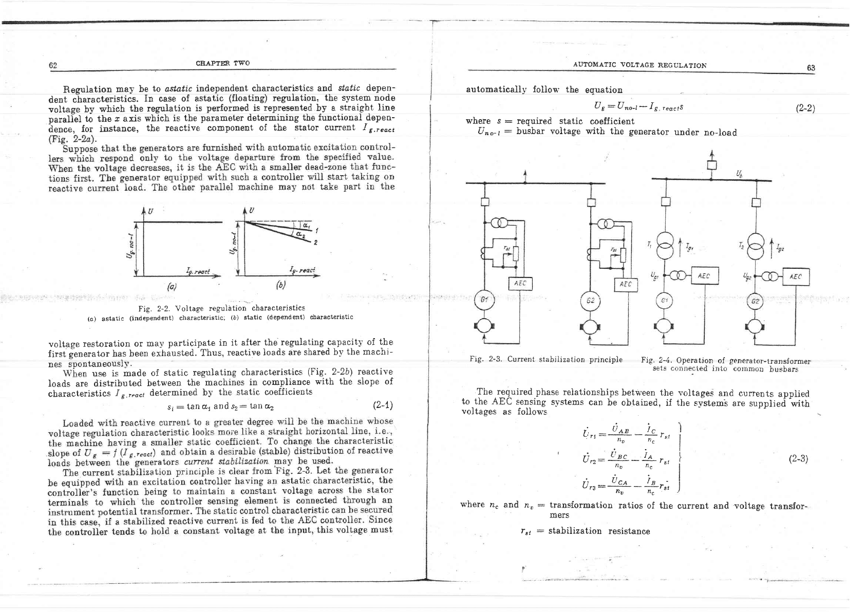
Regulation
may
be
to
astatic
independent
characteristics and,
statlc
depen-
dent
c-haraeteristics.
In case
of astatic
(floating)
regulation,
the system node
*^I+-^^ l,*' *'lrinh lho rornrlafinn ic nerfnrmad is tcnrcsentcd hv e straight line
v
\rrue6e
ryJ
n srvs
-I- ----'-'
-
J
parallel
to
the
s
axis
which
is
tbe
parameter
determining
the functionai
depen-
-J
-- - - f^- :-F+^h^^ *1-^ -a^a*it'a ^^m-nnanf nf f l"o cf of nl arrmanf I
(lguc!
fUL
IllD!alUfrgt
uIl9 lsavel
Ye
vvsPuussv
vr
uLe
eeqvvr
-
g.f
eOCt
Fig.
2-2.
Voltage
regulation
characteristics
(a)
astatic
(independent)
characteristic;
(b)
static
(dependent)
c'baracteristic
().-2\
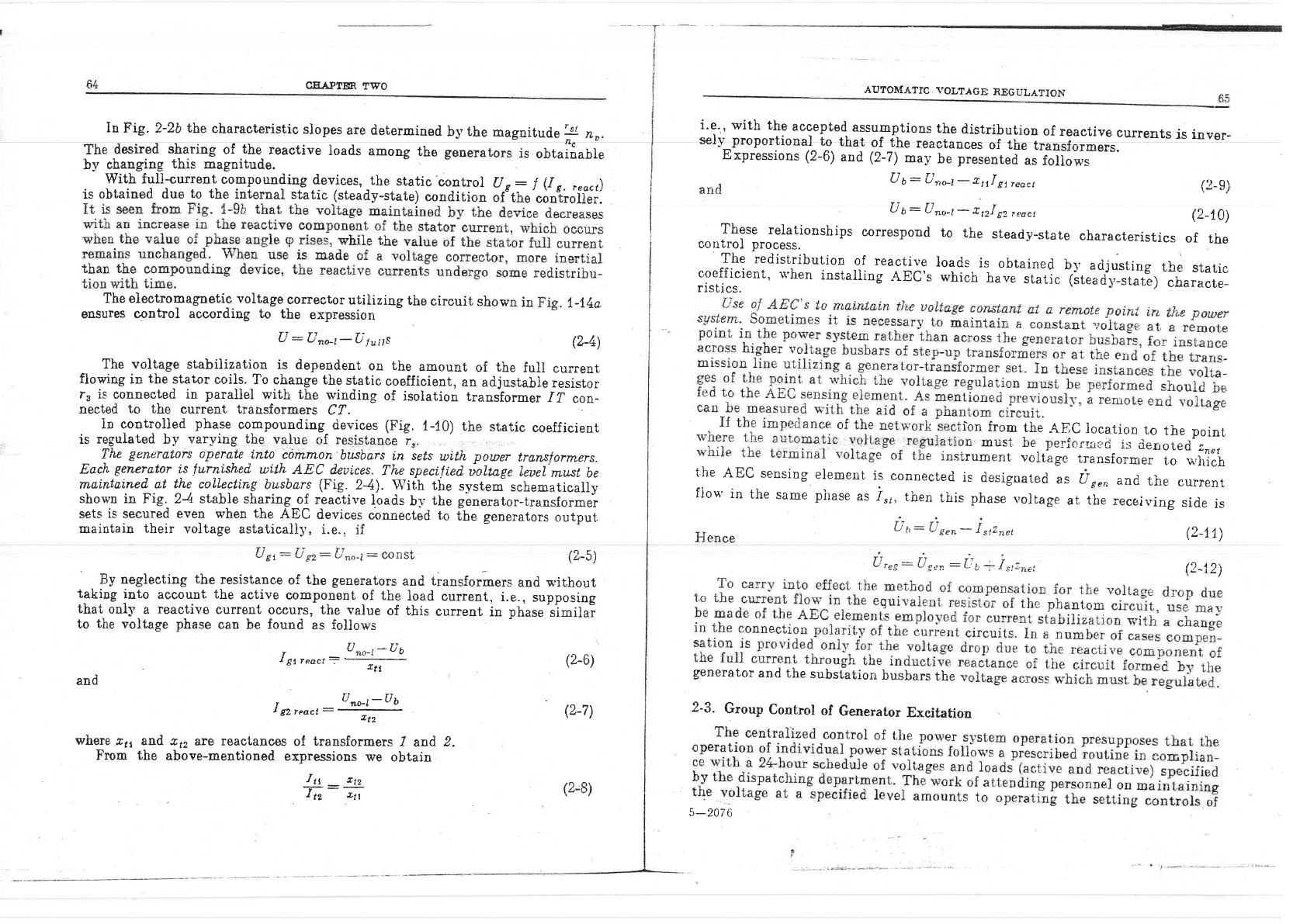
Fig. 2-3.
Current
stabiiization
principle
Fig.
2-4.
Operation
of
generator-transformer
^^4^
^-.---^^r^J i.-a- ------,,, t t
DTTi
UUIIIIUULU(I
III LU
(.;UIITIUOO
I]USDATS
the.ryquired
phase
relationships
between the
voltages
and
currents
appliecl
to the AEC
sensing
sJ*stems
can
be obtained,
if the
-.-vstem-s
are
supplled
witU
voltages
as
follows
L,t:+t
:
J-9-
,*
tlo
nc
'
ri
-
L'nc
in
v
r2-
,r, -l
'"t
(Jrs:'u'n
-i"
r:.
",
Tl'st
where zc
and
fto
:
trans{ormation
ratios
of
the
mers
rsr
:
stabilization
resistance
AUTOMATIC
VOLTAGE
REGULATION
63
automatically follow
the
where s
:
required
static
Uno-t: busbar voitage
equation
Ue:Uno-t-f
g
reacrs
coefficient
with the generator
under
no-load
voltage
re-qtoration
or
ma-v
participate
in it
after
ths regulating
,capacit,y
of
the
first
ienerator
has
been
exhausted.
Thus,
reactive
}oads are
shared b-v
the
machi-
nes
sDontaneousl]'.
Wiien use i-q made
of
static resulating
cbaracteristics
(Fig
-
2-2b)
load.s are
distributed
between
the
machines
in compliance
with
the
characteristics
/g.r"ocr
determined
by
the static coefficients
si
:
tan
&1 drrd -cz:
tart
a"
reactive
slope
of
(z-1)
(2-3)
current
and voitage
transfor-
-- - 'r'
'-
CEAPTSR.
Tq/O
In
Fig. 2-2b
the
charaoteristic
slopes
are determined.
by
the
magnitude
3
n".
The
desired
sharing
of
.the-
reactive
load.s
amoDg
the
geuerators
is
oftaliulie
by
changing
this
naagnitudo.
ctrangrng
t-nrs
Eeagnltud.s.
with full-current
compoun{iug
devices,
the
static
'coatrol
U
s:
f
V
e.
,"oct)
is
obtained due
to
the
in'ternal st"atic
(steaay-s1;;;i-;";dr;i;;
;ftrhr'd"1;.in#l
U
:
Uno-t-U
l.'tts
1-14a
(2-4)
i'e',
with the
accepted
assumPtion-s
the
distribution
of
reactive
currents
is
inver-
sely' proportional
to
that
of ihe
reactances
of the
transformers.
Expressions
(2-G)
and
(2-z)
may
be
p.r.*orcJ
as
forlows
ALI?OMATIC
VOLTAGE
REGULATION
and
Hence
These
relationships
correspond
control
process.
U
u:
Urrnt
-
rttl
s,
,oo",
U
t:
a
ro-t
-
rtzf
E2
react
Ti- -Ti f
o'
h:
U
Etn-
l
slZnet
U
res:
U
sun
:
t]l
r-
j
*znet
to
the
steady-state
characteristics
of
the
b1'
adjusting
the
static
(stea
d1'-state)
characte-
(2-e)
(2-10)
The
redistribution
of
reactive
loads
is
obtained
coefficient,
u'hen
installing
AEC's
whicli
have
siatic
ristics.
The electromagnetic
voltage
conector
utilizing
the
circuit
shown
in
ensures
control according to
the
expression
The
voitage
stabilization
is dependent
on
the
amount
of
the
fuII
current
fiowing
in
the
stator
coils.
To change
the
static
eoefficient,
aD.
adjustable
resisior
r, i's
c'onnected
in
parallel
with the
winding
of
isolation
translorm
er
I
T
con-
nected
to
the
current traasformers
CT.
In controlled
pha-se
compoupding
devices (Fig.
1-10)
the
static
coefficient
isreguIatedbyvarvingthevalueofresistance},.
Th,e
gentrators
operate
i,nto
common
busbars
i,n sets
wi,th
power
traruslorrrlers.
Each
gener-ator
i_s
furnish,ed
wi.th'
AEC
dcutces.
Th,e speci.f
ted
ioltage
Leuel
mu,st
be
maintai,ned at
th'e.
collecting
busbars
(Fig.
24).
With
tire
system
schematically
shown
in Fig. 24 stable
sharing
of
reactive
ioads
b1'
the
glnerator-transformer
sets
is secured even
when
the
AEC
devices
connected
to
ihe
generators
output
maintain
their
voltage
astaticall5',
i.e.,
if
r'on
from
the
AEC
location
to
the point
ln
must be.
perfoli:rcl
is
iierroted
in"r
trument.
voitage
transformer
to
t,Iiilh
the
AEC sensing
eiemett
is
connected
is
designated
as un"n
and
the
current
flou'in
the
same
pirase
".
ir,,
then
this phase
volLage
at
tlie
receiving
side
is
ll-.:fi -...-f'f
.-.^nci
-87
"gZ-vno-t-
vvrrou
/q
r\
\L-o )
(2-6)
(2-7)
(2-11)
ln tq\
\L-tz)
By
neglecting
the
resistance
of
the generators
taking
into
account
the
active
component
of the
that
only
a
reactive
current
occurs, the value
of
to
the
voltage
phase
can be found
as
follows
r"'*o"'=ry:"
and
I
92t..,ct
-
uno'I-ub
xt2
where
rs1
and Etz
ate
reactances
of transformers
I
and
2.
From
the
above-mentioned
expressions
we
obtain
4:e
t
tz
xll
and
transfor-mer-"
and without
Ioad
current,
i.e.,
supposing
this
current
in
phase
similar
generator
and the
substation
busbars
the
2-3.
Group
Control
of
Generator
Excitation
s-2076
CEAPTEN
TWO
the
AEC
devices
in
due
time.
lvith
compound"ing
devices
having
a
voltage
correcror,
attendini
;;;"ffii
"h.og.
int
it"o*orhation
ratio
of
the
setting
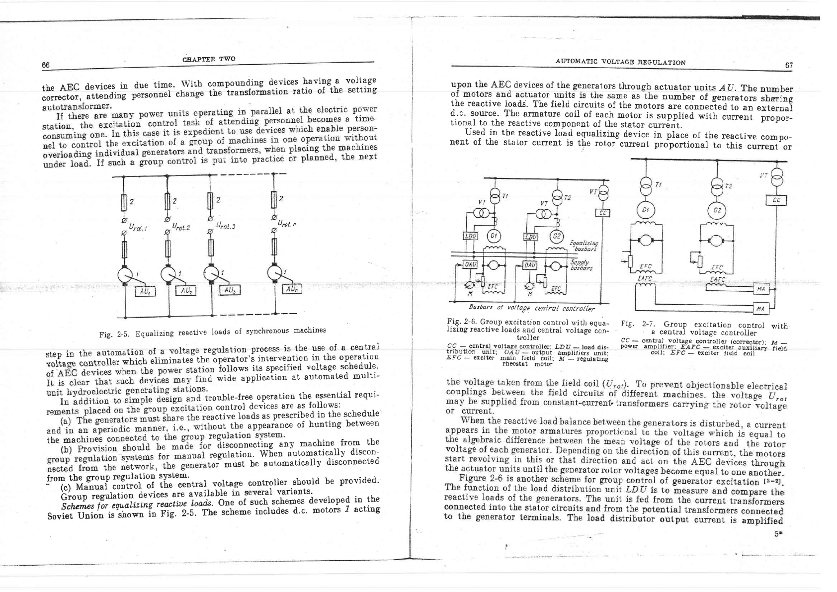
Fig.2-5.Equaiizingreactive]oadsofsynchronousmachines
crpn in the. automation
of
a
voltage
regulation.pr.ocess
is
the
Ptt,of
"::l:l{
:-:d^: .^-r'.,11o" which eliminates
the
operator's
interventrgn
r+
lrte
oP€raLr{ru
L
iollows
its
specified
voltage
sched'ule'
w-ide
applicaiion
at
automated
multi-
cuble-free
operation
the
essential
requi-
control
devices
are
as
follows:
rctive
loads
as
prescribed
in
t'he
s-chedule
out
the
appearance
of
hunting
between
egulation
sYstem.
disconnecting
anl'
machine
from
the
egulation'
Wben
Cutomatically
discon-
rr"
must
be
automatically
disconnected
from
the
group
regulation
sYstem'
-
(c) Manual
-.;;;;;i';;
lil'
"*ottal_
volra.ge
controller
should
be
provided.
Group
regutaiion
devices
are
available
in
several
variants'
Schcmes
far
equalizing
reactntlooiibne
of
such
schemes
developed
in
the
soviet
union
is
lhown
in
Fig.
z-i.
-ru"
scheme
incrudes
d.c.
motors
-z
acting
i
t
Unt.n
AUTO}IATIC
VOLTAGE
REGULATION
67
upon
the
AEC
devices
of
the generators
through
actuator
units
Att.
The
number
of
motors
and actuator
units
is
the
same
a-q"the
number
of
g""rr"tors
sharing
the
reactive
loads"
The
fieid
circuits
of the
motors
are
connected
to
an
external
f,,l; ;"Xt
"T:
:1n; ::T :* :t ^::l^y:.":-
i s-.sup
p.I
i'
a *itt'
"u,""o
t
pro
p
o
r-
^vuvv^
vv
vvspvuesu (,r
Llr'
DtULUI'
Gu.rrgnL.
Used in
the
reactive
load equaiizing
device
in place
of
the
reactive
co'po-
nent
of
the
stator
current
is
the
rotor
current
proportional
to-i[is
current
or
Dusoars
of vcttage
ceniral
canirol(er
Fig.
2-6.
Grgup_ excitation
controi
n,ith
equa-
Iizing
reactive
loads
and
central
voitage
con-
trol I er
CC
-
central voltage
controller;
LDU
_
)oad
dis_
tri_b_utron
unit;
OAU
-
output
amplifiers
unrr:
Err'c
-
exclter
T.Sg"_l,..rd_:gil;
M
-_
resutatins
r uvu-ra
I
luu
Lul
Fig.
2-7.
Group
excitatjon
control
q,ith
-.q
-
a centrai
voitage
controller
-!-C
-
cenL-3]
voltage_c-ontroller
(corrector):
M
_
power
ampllf ler:
-E,4.FC
_.exciler
.auxiliarf-
]leld
coil;
EFC
-
exciter
field coii
'
'
ATTTOJ\IA?IC
.I"OLTAG
g
REGULATION
69
68
CEAPTEN
T.wO
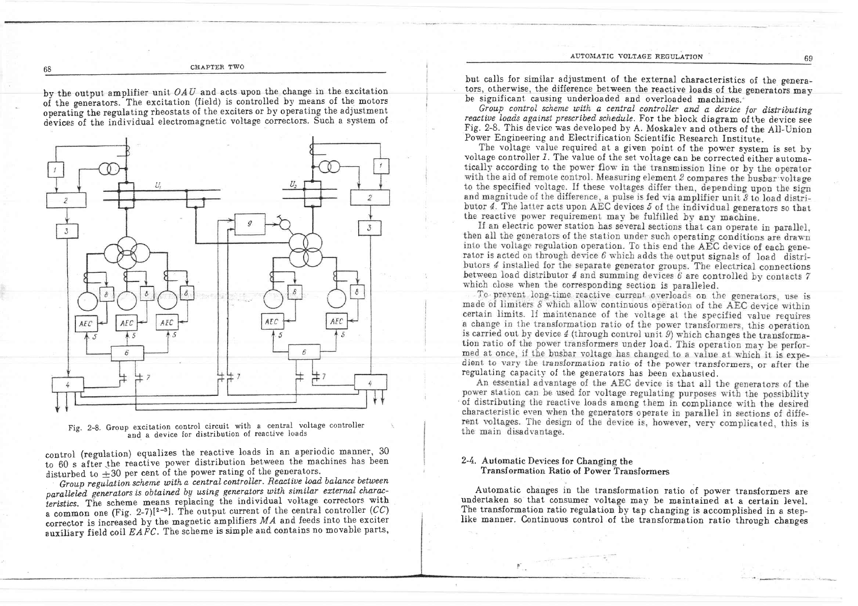
by
the output
amplifier
unit O,4
U. an_d
acts
upon
-the
change
in
the
excitation
of
the
generators.-The
excitation
(field)
is
controlled
by
means
of
the
motors
operatiig
the
regulating
rheostats
of
the exciters
or
b-v operating
the adju-stment'
device-" Jt tne
individual
eiectromagnetic
voltage correctors.
Such a
system of
Fig' 2-8'
*"ou
o",ii"i'T:""il"f;';'"i,,ffi
l,
"Nt
:1
'l, ;;H1L,I!
t'u*' co n
tro'er
control
(regulation)
equalizes
the
reactive
ioads
in an
.aperiodic
manner, 30
;;10
*
Iftl"r
Jhe
reacfive
power
distribut.ion
between
the machines
has been
disturbed
to
+-30
per cent
of
the
power
rating of
the
generators.
-
--l
Group
regulation
sch,emc
with
a
central
controllcr-
Reactiue
Load balarue
between
naralleled.
g-encrators
i.s obtai.ned
by
using
generators wtth
similar
etternal
ch'arar-
irriiit.
Tire
scheme
means
replacing
the
individual
voltage-
correctors
with
*
""**o"
one
(Fig. 2-7)Iz-81.
The
output
current
_of
tire central
controller
(CC)
corrector
is inoreaJed
by
the
magnetic-amplifiers
MA
and feeds
into
the exciter
,"iiri"ry
iield coil
EAFC.
The
siheme
is
simple
and
contains
no
ncovable
parts,
but calls
for similar. adjustment
of
the
external
characteristics
of
the
genera-
tors,
otherwise,
the difference between
the
reactive
loads
of the generatois
may
be significant causing
underloaded
and
overloaded
machines.
-
Group
co-ntrol
scheme
u;ith' a
central
controller
and.
a dnuice
lor
distributing
reafiive loads
agairut prescribed
sch,edule. For
tbe
biook
diagram
of tbe
device see
Fig. 2-8. This device
Eas
deveioped
b:v A.
tr{oskalev
and
ofhers
of
the
Ail-Union
Poq'er Engineering and Electrification
Scientific
Research
Institute.
-
The
voltage- value
-requireti
at a
given
point
of
the
pou:er
system
is
set
by
voltage
controller
I.
The
value
of the set
voltage
can
be
cbrrectedeither
automa--
:^'::,i^;L:':i_:::.:':;";;^^-:"i::^i:_":".::,-'_"^_v"_*:', l::."i""ruers'
ur
arrEr ''Ie
rcEurd.urrrS
L,dp.rL.r[.!
Ui
r,uE
gt,rttrtdLUr'] UaS
ljue11
e)rI]aUSIgO.
2-4.
Automatic Devices
for
Changing
the
Transformation
Ratio
of Power
Transformers
Automatic changes
in
the
t.ransformation
ratio
of
power
transformers
are
undertaken so that
cotrsurner
voltage
may be
maintained at
a
certain
ievel.
The
transformation
ratio regulation
by
tap
changing
is
accomplished
in a step-
like manner.
Continuous control
of the
transformation
ratio-through
changis

/U
CEAPTER T'WO
in the
magnetic
state
of
the
magnetic circuit
b-v
magnetizing
it
is
sometimes
used
for
low
rated trausformers intended
to
handie
special loads.
_
When-designing
the sensing element
of
the reguiator
step-like
changes
in
f ho trondfnnmof inn nqf in ^{ ^rtlinor-' hnntol lronc{ar*^-.
"*,1^-
I^^ J *--^r L^
'vru^!qr
!t lru
?vv!
!rsl'DrvluErJ
t
tltrsl rudu
ll_lust
Irg
taken
into account.
The regulator
must
have a
dead zone
which
overlaps
the
vcltage
overiegulation
value
afier the reguLating
deviee
is switched
tirroueh
one
step.
Reguiation must
be
slow in
order to
prevent
the
switching
device
from
o-perating during
sbort-time
voltage
variations
as
frequent
operation
m.ay damage
the
mechanism. The
output
control
signal
is
usually executed
within
20 to
30i.
The
sensing eJement of
thp
regulator
can respond
to a
change
in
the voltage
at
the reguLator location,-
to
a change in
the value
of the
vector
voltage
sum
ai
the
regulator
position
q'ith
a_
voltage
drop
because
of a
current flow
in
an
equiva-
Ient resistot, i.e., to
a
cha_nge in
-the
voltage
at
a
certain point
in the power
srrstem electricaliy
ciose
either
to
the load-centre
substation
or to the
connection
point
of
the
current
teceivers, and
to
a
change in the
vaiue
of the voltage
at the
reguiator
position s'ith
a comection
by
the
value
of
the
current
fiow
in
the
feeding line or by
tbe
value
of
reactive
power.
To
control
the transformation
ratio,
when
under
load,
the
transformer
tap-
changer
position
is sometimes
changed aiso
aufomatically
b-v
a
programmbr
insfalied at
the substation
or
at the
operator's point,
to
follow
an hour
sihedule.
for inslance.
When a
trausforner
with autorr.ratic
coniroi
of the
transformation
ratio is
installed
at
the recsiving
consumer
substation,
it is
better
to
accomplish
the
voltage
regulation
together
with
the
correction
of the
current
flowing
in
the
feed line or the
value
of
reactive power.
If
such
correction
is
not
used,
then,
tending to
maintain
a consLant
voltage
across the
consumer
terminals
in case
of
a drop-in the
voltage
due to increased
losses
when
the
load gro\I,s,
the regula-
tor
switches
over
tbe regulating
device
of
the
power
transformer
in
order
to
rcdrre.e the transformation rat.io.
The
result
v.'ili
be
an lncre*se
in
the
currenr,
fln'rxrino f hr^ttoh +ho foorl li-o o-d o rlrli*innol l^oooo -,i+1. *"-+1-^- -^1.,^+: ^* ^!
vs^vu6u uusrervuqr
tvoovD wruu
lua bugl
ltt(luul,lull
ul
the voltags
across
the
terminals
of
the power
transformer.
,A.Iong
with
the
principle
of
reguiating
the
voltage
by following
its
devia-
the regulating
principle,
the_
control
system
must
maintain
the
voltage
within
the limits
permitted
by
the
load of the
power
system
region.
, Let the voltage
regulator
priucipie
be
studied
on the
basis of the
TsSRZAI
type
(I{CPBAH)
regulator known for
its
simp}e
construction
(Fig.
2-9).
The
controlrela-vs
lCR
asd,2CR
co^nt1oi
tb-e
tap
changer
of the power
trans-
former
b.-;i means.of
auxiliary
relays
TAR
and
4iR
andtime
relaf
iTR.
fbe
relav
coils
are fed with
a.c. power.-Relays
lCR
and 2CR
are two-co'it
polarirea
(b)
ror
,.u,-"lr"e;,?;?;J1iT:Hfftil"":,,:,T,T::,t
!!,
^ u ,",
relays
(tbe
coils are
in
opposition).
Under
normal
cond.itions
the
resultant
emf
of
_the
rela-v
armature
is equal
t_o zero
and
its
contacts
are
opened.
One of the
coilsof
r-elays
lCR
and
also
of 2CR
are connected
through
r*ititirtr
to the
ter-
minals
of
the
instrument_voltage_transformer
VT
in series
with
tbe windinj
ot
a
guickly^
saturable
transformer
^S?.
Depending
upon
the value
of
terminai
vol-
Lagg
U
of
the
instrument
transformer
VT,
the-current,.L,
flowlnt
in
one of
the
goilj.of
relays
/Cr?
and
of.2CR
has
a
clearly
nonlinear
Lharacteristic
(curve
-l
in
Fig. 2-9b).
The
other
coils
of reiays-fCfi
and 2CR
arc
oonnected
to
the
second,ary
cir-
cuits of tbe
voltage
transformer
ST
and the
intervening
transforme{
ICT
AUTOMATIC
VOLTAGE
REGULATION
7t
lo)
79 CIIAPTER T\\'O
(Fig.
2-9a). The
primary
of
the transformer ICI'is
connected
to
the
secondary
winding
circuit
of the crurent
translormer
CT.
The behaviour of
the
current.I,
flowing
in the other
coils
of relays
lCR
and
2CR
conlorms
to
cutve
2
in Fig. 2-9b.
The
settings are
adjusted
by means of a
series
resistor and tap
changing on
the intervening
transformers
so that at
the voltage
equal
to
the
set
voltage.
the
currents
,I, and
.I,
equal each
other, Departure
of the
voltage
from the
specified
value
causes
relavs
/C,R
and
2CR ta function.
llorp
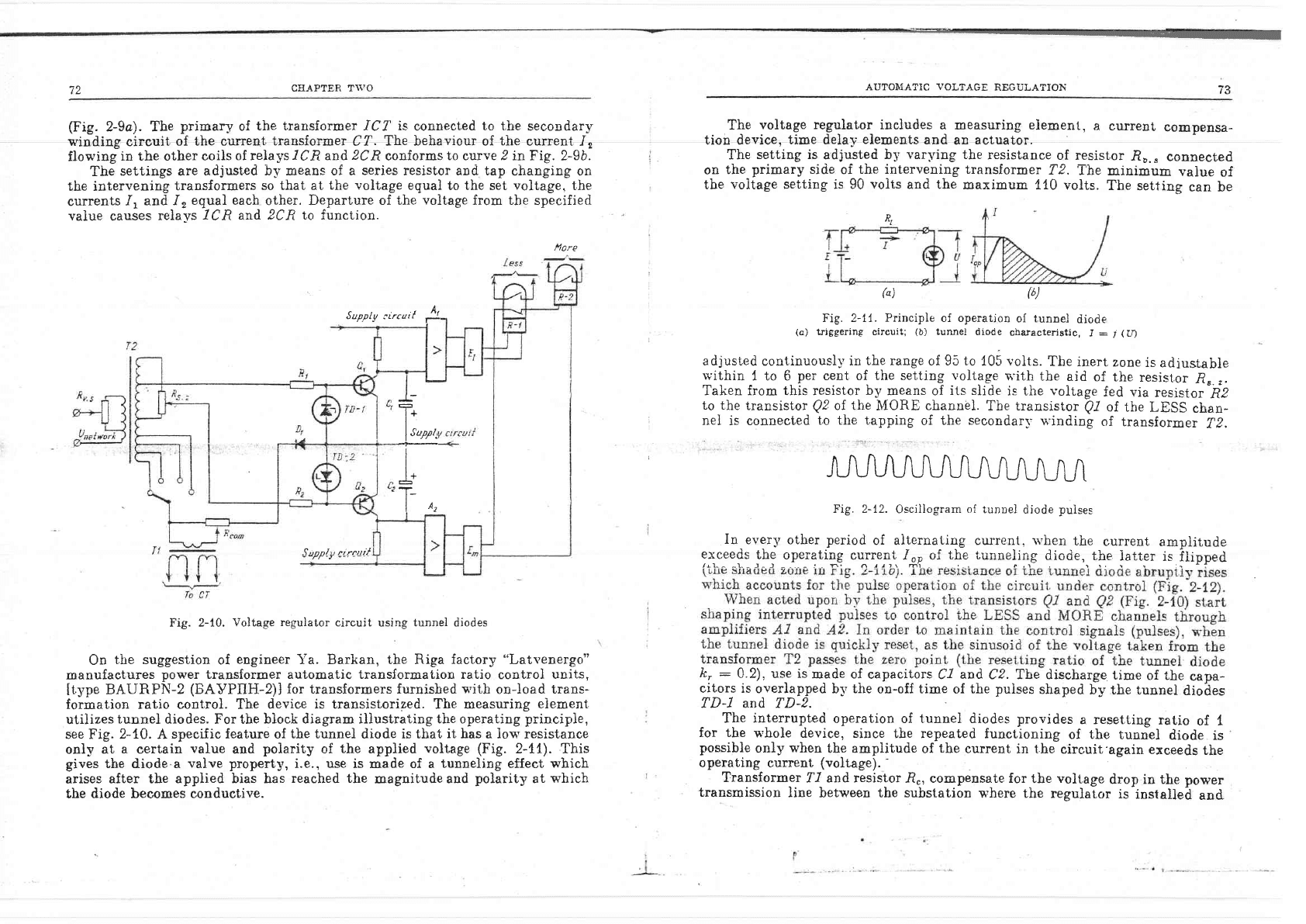
Fig. 2-10.
Voltage
regulator
circuit
using
tunnel
diodes
On
the suggestion
of
engineer
Ya. Barkan, the Riga
factory
"Latvenergo"
manufaetures
power transformer automatic transformation ratio
control
units,
ltype
BAURPN-2
(EAVPIIH-2)]
for
transformers furnished
with
on-Ioad
mans-
formation ratio control.
The
device is transistorized.
The
measuring
eiement
utilizes
tunnel
diodes. For the
block diagram iliustrating the operating
principle,
see Fig. 2-L0. A
specific feature of
the tunnel
diode
is that it has a low
resistance
only
at
a
certain
value
and
polarity
of
the
applied
voltage
(Fig.
2-11). This
gives the diode a
valve property,
i.e.,
use
is made of a
tunneling effect which
arises
after the applied
bias
has
reached the
magnitude and
polarity
at
which
the
diode beeomes conductive.
AUTOI\TA?IC
VOLTAGE
REGULATION
The
voltage regulator includes a
measuring
element,
a curreDt
cornDeDsa-
tion device,
time dela;*
elements
and
an
actuator.
The
setting is
adjusted
by
varyiug
the
resistance
of resistor
-Ro..
connected
on
the
primary side
of
the intervening transformer
72.
The
minimum
vaiue
of
the
voitage setting is 90
volts
and the
maximum
110 volts.
The
settins,
can be
(")
(b)
Fig. 2-11.
Principle
of operation
of
tunnel
diode
(o)
Uiggering circuit;
(b)
tunnel
diode
characteristic,
J:
t(Lr)
adjusted
continuousl-v
in
the
range of 95 to
105
volts.
Tire
inert zone
isadiustable
w-ithin
-1
to 6_
per cent of the setting voltage
with
the
aid
of
the
resist,or
,R".
r.
Taken from this resist.or
by
means
of
its slide
is the
voltage
fed
via
resistor-Ez
to the
transistor
QZ
af. the
MORE
channbl.
The transistor
Q-Z
of
the
LESS
chan-
nel
is connected
to
tlie
tapping
of
the secondar5.
v'inding
of
transformer
Tt.
Fig. 2-12.
Osciliogram
of
tunnel
diode
puises
In
everv other period
of alternating culrent. t'iren
the
current
amplitude
o.'^on.lo +1"^ ^-^-^+i-^ ^.'--^*+ f ^t +].^ +,-**^1:-- l:^l^ aL^ I-r---:- ?r. - r
;:J^""-i:.'1,'-'!-"j1:':q
":":,",\'g? "'
trfv. tru'rru"1'l',H
lttt"',
t1"
aoLteI'
rs
rrlppeo
kt
:0.2),
us-e
is
mads
of
capacitors
CI
and.
C2.
The discharge
time of the
capa-
citors is
overlapped by the on-off time
of
the pulses
shaped
by
the tuunel
dioiies
TD-[ and TD-z.
The
interrupted
operation of tunnel diodes provides
a reset,ting
ratio
of t
for tbe
whole
device, since
the repeated
functioning
of
the
tunnel
diode
is
possible
only
when
the amplitude
of
the
current
in t.he
circuit'again
exceeds
the
operating current
(voltage).
-
Transformer
Tl_and resistor.R'
compensate for
the
voltage
drop in the
power
transmission
line between the substation
where the
regulator
is
instalJed
and
"t
Sup.oty:rrcuil
rlJ
C nnl ninttil
.-L-
F.
l+
I
I
Supplt
T-
I+
!:
-t--
lA,
,2
l.
CTIA?TER T.wO
the
consumer
where
the specified
voltage
is to
be
maintained.
When the
cur-
rent flows ooly in the
primar*v v'inding
of transformer
Ti,,
tbe
i-nternal
shift
angle of
the
current
flowing in
the
secondary
winding
amounts
to 26-30
deg,
this
rietermiaes
^r,he
eounec'r,ion
of
tbe
primarv
-windins
of the
trausformer
Ti t,o the
current
transformer of the lagging
phase.
The
time
deiay
elemeui
made of semiconductor elements
can
provide
con-
tinuous adjustment
for
7
Lo
2 min. Fig. 2-10
shows two time
delay elements
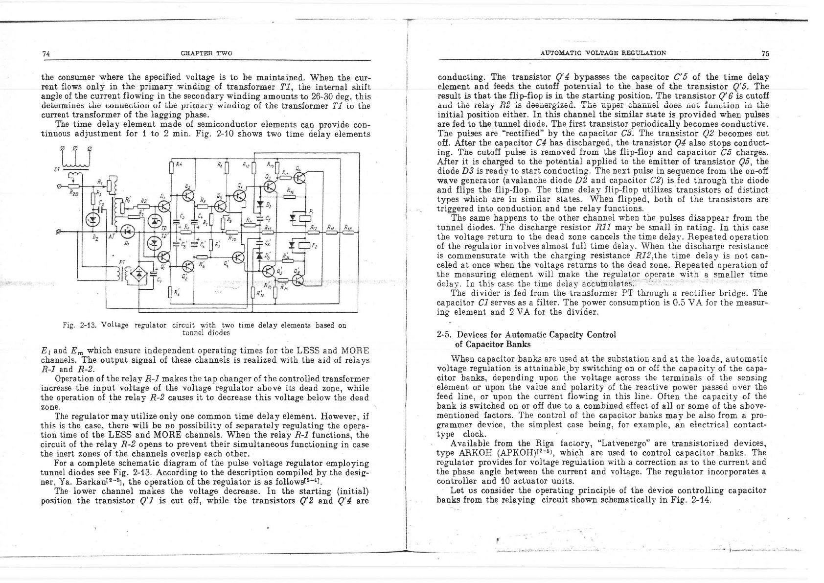
Fig. 2-13.
Voltage
regulatoi circuit with two time
delay
eiements
based on
tunnel
diodes
D ^-J Zr *L:^L
.:-l^-^-J^*+
^-^-^+:*- +:-*^^ 4^- +L^ T [iOC ^-l trr/1Dr}
Itl dlt|.I 12772
vrLLLrtLt
uu.Sl,lltt
rj.tUtrPt;lurrlt, UPt;ra1LIJ.IH
U.tI.Lrt s IUI t,LlE trI]lJLl
anU
IYIL,r-ftEl
cbanneis. The ouiput,
signai
of
ihese
channeis
is reaiized
with
the
aid
of
reiays
R-l
and
R-2.
Operation
of
the relay
l?-/
nakes
the
tap
changer of the controlled
transformer
increase the input
voltage
of the
voltage
regulator
above
its dead
zoue,
s'hile
the
operation of
the relay
.E-2
causes it
to decrease this
voltage
belor*'the
dead
zone.
The
reguiator may
utiiize
oniy one common
'uime
cieiay
element.
Iiowever, if
this is
the
case,
there
will
be
no
possibility
of separately reguiating
the
opera-
tion
time
of
the
LESS
and
h{ORE channels.
When the relay
,R-.2
functions, the
circuit of
the relay .R-2 opens
to
prevent
their
simultaneous functioning
in
case
the inert zones
of
the
channels
overlap
each
other.
For a complete
schematie diagram of the
pulse
voltage regulator
employing
tunnel
diodes see
Fig.
2-73. According
to the
description conpiled
by
the
desig-
ner,
Ya. Barkant2-z1,
the
operation
of the
regulator
is as
folloysfr-a].
The
lower
channel makes
the
voltage
decrease.
In
the
shrting
(initial)
position
the transistor
p'l
is cut off, while
the
transistors
Q'2
and
Q'4
arc
F
AUTOMATIC
VOLTAGE
NEGULATION
conducting. The
trausistor
Q'4
bypasses
the
capacitor
C'5
of.
the
tine delay
element
and
feeds the cutoff
potential
to
the
base
of the
transistor
Q'5.
The
result
is
that the
flip-flop
is in the starting
positiou.
The transistor
Q'6
is
cutoff
^- .] aL- -^]^-- T>O :^ l^^-^--:-^l mL^ ----^- ^L--*^1 l--- -^r t----!: -- :- aL^
auu
Llle fulily
flp
rs
uttruclgrzEu.
rlu
upPvl u!.a!.l.Iur
uueD uu! rrriloLIUrII ru Luc
initial
position either.
In this channel
tbe simiiar
state is
provided
when
pulses
are
fed
to the
t,unnel
diode.
The firsi; iransisior
periodicaily
becomes
conduciive.
The
pulses
are
'tectified"
by t,he
capacitor
C3.
The
transistor
QP
becomes
cut
off.
After
the capacitor C4
has
discharged,
the
transistor
Q4
also
stops
conduct-
ing.
The
cutoff
pulse
is temoved from
the flip-fiop
and
capacitor
C5 charges.
AJter it is charged
to the
potential
applied
to the emitter
of
transistor
Q5,
the
diode
Di
is
ready to start
conducting. The
next
puise
in
sequence
from
the on-off
wave
generator
(avalanche
diode
D2
and capaeitor
C2) is
fed
through
the
diode
and flips
the flip-flop.
The
time deiay fiip-flop utilizes
transistors
of distinct
types which
are
in simiiar
states.
When
flipped, both
of
the
transistors are
triggered
iato conduct,ion
and tbe relay functions
The
same happens
to the
other channei
'when
the
pulses
disappear
from
the
tunnel
diodes. The discharge
resisLor
RLl
ma-v be
small
in
rating.
In this
case
the voitage
retwn
to the dead zone
canceis
the time
delal'. Repeated
operation
of
the
regulator involves almost
full time dela-v.
When
tbe discharge
resistance
is
commensurate
with the
charging
resistance
R[Z,the
time delaf
is not can-
celed at once
when
the voitage returns
to
the
dead zoae.
Repeated
operation
of
the
measuring
element
will
make
the reguiator
operate with
a snaLler
time
deiav. In
',.his
case the
tirre
deiay acc.umulat.es.
'
The
divider is fed from the transformer PT
through
a rectifier bridge. The
capacitor
C-I
serves
as a filter.
The
power
consumption is
0.5 VA
for the
measur-
ing element and 2
VA
for
the
divider.
2-5.
Deviee*"
for Automatie Capaeitv
Control
of Capaeitor Banks
\X7L^- -^-^^:!-- L^-f-- ,] -r rL^ --.L^r^a:^- ^- J -r
rL^
l^^ l- ---r--^4i^
vYttvu
(ialjauruul'lraul{'D
a1ru {rStiu
au
Lutr
suusLaLruu auu
aL
Lutr
luilub,
auLUrrrilurL;
voltage reguiation is attainable.by
switching
on
or
ofJ the
capacit-v of the capa-
citor banks,
depending upotr the
voltage
across
the
term.inals of the sensing
element
or
upon the
value
and
polarity
of tbe reactive pov'er
passed
over
the
feed
line,
or upon the current
flowing in this line.
Often
the
capacitv of
the
bank is switched
on
or off
due to
a
combined
effect,
of all
or
some
of
the above-
ment,ioned factors. The control of
the
eapacii,or banks
may
be also
from.
a
pro-
grammer
device,
the
simpiest
case
being,
for
example,
an electricai contact-
type
clock.
Availabie
from the
Riga
faciory,
"Latvenergo" are
transistorized
devices,
type
ARKOH
(APKOH;tz-s:t, which
are used
to
control
capacitor
banks. The
regulator provides
for
voltage regulation
with a correctiou
as
to the
cu.rrent
and
the phase
angle between
tbe
current and
voltage.
The
regulator incorporates
a
controller
and 10 actuator
units.
Let us consider the operating
principle
of
the
device
controliing
capacitor
banks from the
relaying
circuit shown schematicali5'
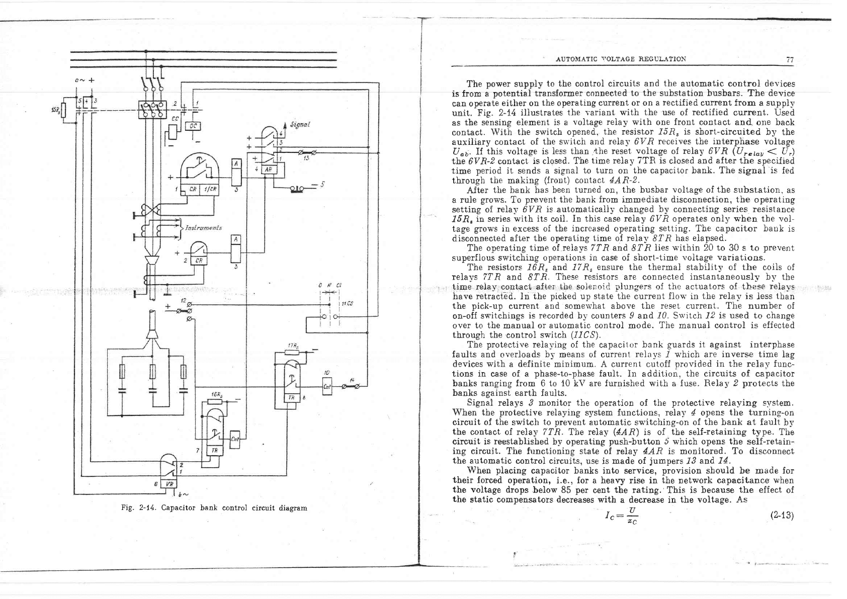
ls Fig. 2-74.
JJ
+
AUTOJ\{ATIC
TOLTAGE REGULATION
The
power
supply
to the
oontrol
circuits
and the
automatic control devices
is
from a
potential translormer conDected
to the
substation
busbars.
The
device
can operate
either
on
the operating
current or on
a rectified
curreut from
a
supply
unit.
Fig. 2-14
iliusfrates
the
r,ariant with the use
of
rectified
current.
Used
as
the
sensing
element
is a
voltage relay with
one
front
contact and
one back
contact.
U/ith
the switch opened.
the
resistor
15fi,
is short-circuited
by
the
auxiliary
contact of
the su'itch and
relal'
6VR
rcceives tbe
interphase
voltage
Uob. If.
this voltage is iess
than.the reset
voltage
of
relal'
6VR
(Ur.roy<-
U,)
tine
6VR-2 contact
is closed. The
time
relay 7TR is
closed and
after the
specified
time
period
it sends
a signal
to turn
on
the capacitor
bank.
The signai is
fed
througir
the
making
(frout)
coutact
4AR-2.
A-fter
the
hank
has been
turned
on,
the busbar
voltage
of
the
substation.
as
a rule
grows.
To
prevent the bank
from
immediate disconrrection,
the
operating
setting of
relal' 6trlft is automaticali-v changed
by connecting serie*q resistance
15R,
in series
*-ith its
coil. In
this
case relay 6P-R
operates onll'when the
vol-
tage
grows
in excess
of
the
increased
operating
setting.
The
capacitor bar:k
is
disconnected
after the operating
time of
rela-v 8fR
has
elapsed.
The
operating
time
of
reiays 7TR and
8?R
lies
u'ithin
20
to
30
s to
prevent
superflous
switching
operations
in
case of short-time
voitage
variations.
The
resistors
l6-R, and
17ft,
ensure
the
thermal
stability of the
coils
of
rela-vs
7?F and
8f,R.
These
resist.ors
are connected instantaneousl3' |1' 15.
time reia-v contact aJter the
solenoirl
llungers
ol the
actuators of
tLrese
relavs
have
retract€d.
In
the
picked
up
state the
current
fiorl
in
tiie
relas is
Jess
than
the
pick-up
current and
somen'hat
above the
reset
current. The number
of
on-off
switchings is
re.corded
b5' counters 9 and
70.
Srvitch
/2
is used to change
over
to the
manua]
or automatic
control mode.
The
manual control is
effectJd
through the
control
switch
(11C5).
The
protective
rela,ving of the
capacilor
bank
guards
it against
interphase
faults
and overloads
b1'means
of cument
rellvs.l s'hich are inverse time
lag
devices
with
a definite m,inimum. A
current
cutoff
rrrovided
in
the relai' func-
tions in case of a
phase-to-phase
fault.
In addition.
the circuits
of capacitor
banks ranging from
6
to 10
k\z are
furnished with a fuse. Relal'
2 protects
the
banks
against
earth
faults.
Signai
relays
3
monitor
the
operation of
the
protective
relaying s)'stem.
When the
protective
relaying
system functions.
rela-v 4
opens
the turning-on
circuit of
the
switch
to prevent
automatic sv'itching-on of
the
bank
at
fault
by
the
contact
of rela1.' 7TR. The rela-v
(4AR)
is of
tbe self-retaining
type.
Tlie
circuit is
reestablished
by
operating
push-button
5 u'hich opens
the
self-retain-
ing
circuit. The frrnctioning
state
of
relay
4AR
is
monitored. To
disconnect
the
automatic control circuits,
use is
made
of
jumpers
13
ard 14.
When
placing
capacitor
banks
into
service,
provision
should he made
for
their
forced operation,
i.e.,
for a heavy
rise in
the
network
capacitance
when
the
voltage
drops
below 85
per
cent
the
rating. This is
because
the
effect
of
the
static
compensators decreases
with
a decrease
in
the voltage.
As
i1
TU
It\:-
-tc
(2-r3)
Fig.
2-14.
Capacitor bank control
circuit
diagram
78
CEAPTER
:rWO
tbe
currenL
f
"
decreases proportionaliy
when the
volta
ge
[]
drops
with inva-
riant
u
s,
which
causes
additional
reactive
losses
and
a
filrther
drop
in
the
vol-
tage,
i.e., the
process
attains
an avalanohe
character.
This voltage
drop
c.an
be
A
R
L
stopped
b,w an
abrupt
drop
of
theeg
value,
i.e.,
by
an abrupt
insrease
in the
current
-Is
and
reduction
of
the
reactive
losses.
A-u
increase
in
the
capacitance
current
is
attai-
nabie
by
switching
on
additional
capacitor
banks
o-r
by switching
over the
capacitors,
ls
per
scheme
shown
-in
Fig.
2-15,
from
the
interphaje
voltage,
when the phase
current
is
,
BUpn
r;
J
e:
-;--
:
1.5
-
Pn
-
acc
EC
to
the phase
voltage,
when the
phase
current
be-
comes
equal
to
,
Uph
nUph
-. _:
:
_
-
v
0.529 rg
(2-1s)
This sn'itching
operation
is
effected
throueh
switch
2.
2-6.
Voltage
Regulation
by Booster
Translonners
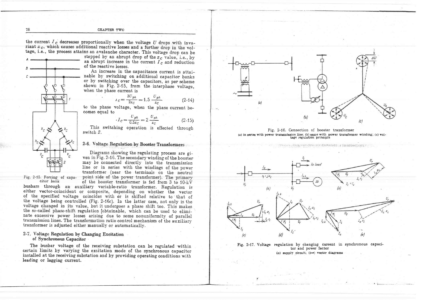
DiagraTs
showing the
regulating process
are gi-
ven
in
Fig.
2-16.
The secondarS'winding
of the
boosler
may
be connected
directly
into the
transmission
]ine or in
series
with
the
windings
of the power
transformer
(near
the
terminals
on the
neutra]
2-15..Forcing
of capa-
point
side
of
the
power
transformer).
The
primary
cir.or
bank
of
the
booster transformer
is fed
from
B'r-o
iO_kt
busbars
througb
an
auxiliar5.
variable-ratio
transformer.
RezuIation
is
either vector-coincident
or
composite, depending
on u'hether
tne
vector
of
the
specified
voltage
coincides
$'ith
or
is
shifted relative
to
'that
of
the
voltage
being controlled
(Fig.
2-16c). In
the
latter case,
not
oniy
is
the
voltage
changed
in
its
value,
but
it
undergoes a
phase
shift
too.
Tiris makes
the
so-called phase-shift
regulatiou
[obtainable,
wbich
can
be
used to
elimi-
nate
excessive power
losses arising due to
some
nonuniformity
of
parallel
transmission
lines.
The
transformation
ratio control mechanism
of the
auxiliarv
transformer
is adjusted
either manually
or automatically.
\roltage
Regulation
by
Changing
Excitation
of Synchronous
Capaeitor
The busbar
voltage
of
the
receiving
substation
can
be
regulated
within
certail
limits
by
varying the
excitation
mode
of
the
synchronous
capacitor
installed at
the
receiving
zubstation
and
by
providing
operating
conditions with
Ieading
or lagging
current.
(2-14)
tsJ
(')
Fig.
2-17. Voltage
regulation
by
changing
tor and
power
current in synchronous
capaci-
factor
(c)
Fig.2-16.
Connection of
booster transformer
(s)
in
B€rie6
witb
power
trarmiesion line;
(b)
eane
with
power
bansformer
wlnding;
(c)
vol-
ra€B regulation
principle
(d)
(a)
supply circuttl
(H)
vector diagrame
:E0
CEAPTER.
T.wO
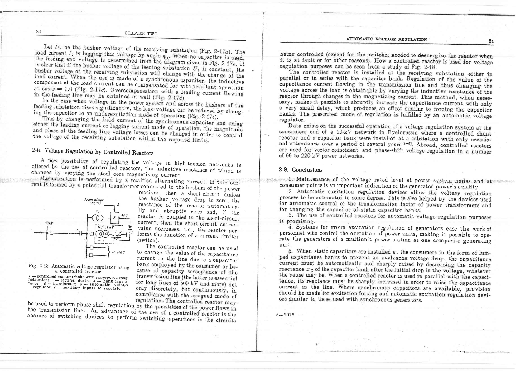
2-8.
Yoltage
Regulation
by
Controlled
Reaetors
Lnput.<
|
6
reaciance
of
the
reactoi
automatica_
y
A .-.
Ih'
.and.
abruptly.
rises
,ua,
li-'tn,
Fq
s
f\ ::i:::l
':,::iti-1,"1
iHg
si,ort-circuit
I f
nln_"_F_.
* ::;-.-"^"uj-urrEu
ulle
,bltorf,-Cttoutt
CUnent
---i
giI",.H:
'l..:l""X'.*ili"'l1i.i:ffillffJ;
2-9.
Conelusions
AIIfOId.f,TIC
VOLTAGE
RE&I'LArION
/t
Rvcfornc for rrrnrr- avnifo*i^-
--
vrt
vavl
uq
vlvu
personnel
who control
the
operation
-^^,,1-+{^- ^c ^^-
rsSuraLrul-r
ul
Et
utsrauul__\
gasg
[I}e
woIK
oI
of.
poi*'er
units,
making
it
possibie
to
ope-
rate
the
generators
of
a
multiunit
power
station
as
one
composite
generating
uo"it.
ie
voltage
in
high_tension
networks
is
rs,
the
inductive
reactance
of
wlrich
is
3netizing
current.
ctified.
alteraaiing
curreut.
If
this
cur_
lr
connect,ed
to
the
busbars
of
the
power
receiver.
tiien
a
short_circuit
makes
frcm other
the
busbar
^
voitage
d.rop
to
zero,
tire
8t
component
of the
load
curuent
can
be
cr
"1.'MaiutorlrBoei'of
tbe
voltage
rated
level
at power
s-I,s1.em
nodes
and
-j".r.
ruarsesrrd.uuril
ur
r.j_lLi
vurr,argc
rat,{ru
!eveI
ai
pOWeI
5-'115.l,€11L
nOdgS
and
at
consumer
points
is an important
indication
of
the
generated
Dower's orralitr,.
ra
ll--ry
(sw[,ch)'
-l
'. .
-
?he
controlied
reactor
can
be
used
I _ l
ne
conrrolled
reactor
can
be
used
|
lc
lood
to
change
the
value
of
the
capacitance
r
current
in the
line
due
to
a
iapacitor
L^*I- ^--l r r .,
ator
usinc'
Fig.
2-18.
Autornatic
vo-ltage
regulator
using
a
controlled
reactor
J
-
controlled
reactor
(choke
wjth
superposeC
mag-
netization);
?
-
rectitier
device;
.?
_
f dnk
cl
i;;;;-'
4:'
:-t-*i,tiii#.;
r
.-
automau"
"ifrl?i
re8ulator;
6
-
auxiliery
inputs
to
-regutaior
b-e
used to
perform
phase-shift
rezuIatior
the
transmission
lines.
An
advantage
r
absence
of
switching
devices
to
peifor
6-2A7 6