Cao Z. (Ed.) Thin Film Growth: Physics, materials science and applications
Подождите немного. Документ загружается.


© Woodhead Publishing Limited, 2011
288
12
Polarity controlled epitaxy of III-nitrides and
ZnO by molecular beam epitaxy
X. Q. Wang, Peking University, P. R. China and
a. YoshikaWa, Chiba University, Japan
Abstract: This chapter discusses the polarity controlled epitaxy of iii-
nitrides and ZnO by molecular beam epitaxy. The chapter rst explains what
the lattice polarity is and reviews the available detection methods for the
polarity. after a brief introduction of the polarity behavior at heteroepitaxy
and homoepitaxy, the chapter discusses the polarity controlled epitaxy of
gan, aln, inn and Zno, paying special attention to inn.
Key words: polarity control, epitaxy, iii-nitrides, inn, Zno.
12.1 Introduction
III-nitrides and ZnO are very promising materials which have many
applications in for example, solid state lighting, full color display, laser
printers, and high density information storage. These materials all have a
wurtzite lattice structure, with lattice polarity along the c-direction, the most
usual growth direction in their epitaxy. Polarity plays an important role in
the epitaxy since the growth mode/behaviors, surface morphology, crystalline
quality, doping ability, chemical and thermal stability are all inuenced by
the polarity. In this chapter, we introduce the polarity controlled epitaxy
of III-nitrides and ZnO grown by using molecular beam epitaxy, paying
attention to how to control the polarity on non-polar sapphire substrate and
the effect of the polarity on sample properties. Section 12.2 briey introduces
what the lattice polarity is and how to detect it. Section 12.3 illustrates the
polarity control in heteroepitaxy and homoepitaxy, in particular the former.
Section 12.4 briey demonstrates the polarity controlled epitaxy of GaN and
aln. This section is not discussed in detail since gan and aln have been
studied extensively. We discuss in detail polarity controlled epitaxy of inn
in section 12.5 including its p-type doping because research into this has
recently become very topical and inn is the most mysterious material of
the III-nitrides. Section 12.6 shows the epitaxy of ZnO, where the polarity
control issue is more complicated than for III-nitrides. Finally, we present
our conclusions in section 12.7.
ThinFilm-Zexian-12.indd 288 7/1/11 9:44:14 AM
289Polarity controlled epitaxy of III-nitrides and ZnO
© Woodhead Publishing Limited, 2011
12.2 Lattice polarity and detection methods
Crystals with wurtzite lattice structure such as III-nitrides and ZnO are polar
crystal along the c-direction, and lacking inversion symmetry along this
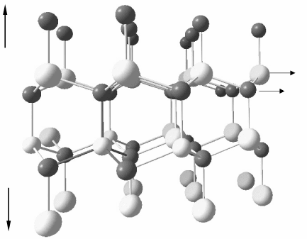
direction. These crystals or lms are either +c polarity or –c polarity. Figure
12.1 shows a lattice structure of a hexagonal crystal, for example, GaN. It
is shown that the lattice polarity can be easily claried, that there is only
one dangling bond along the +c polarity for a Ga atom, while three dangling
bonds are available toward the –c direction. Lattice polarity is an important
issue in the wurtzite semiconductor epitaxy since the growth behavior and
properties of these semiconductors (thermal and chemical stability, optical
properties, surface properties, etc.) are greatly affected by the polarity. For
example, III-nitrides are usually grown on +c-polarity where the growth is
under step-ow mode and atomically at surfaces are obtained. On the other
hand, the –c-polarity usually leads to rough surfaces. Thus, it is important
to perform epitaxy under controlled polarity.
several methods have been established to detect the lattice polarity. They
include chemical etching, convergent beam electron diffraction (CBED),
coaxial impact collision ion scattering spectroscopy (CaiCiss) (Wang and
Yoshikawa, 2004), surface reconstruction revealed from reection high-energy
electron diffraction (RhEED), and circular photogalvanic effect (CPgE).
Chemical etching is a simple method to detect the polarity, but destroys
the sample. Due to the chemical nature of different polarities, the chemical
stability varies. For example, +c-polarity iii-nitrides are more chemically
stable and more difcult to be chemically etched than the –c-polarity ones.
And the step-ow-like morphology usually keeps well for +c-polar samples
except that etching pits appear. on the other hand, hexagonal islands are
+C
–C
N
Ga
12.1 Schematic illustration of wurtzite GaN in different polarities.
ThinFilm-Zexian-12.indd 289 7/1/11 9:44:14 AM
290 Thin film growth
© Woodhead Publishing Limited, 2011
usually observed in the –c-polarity case, which is accompanied by roughening
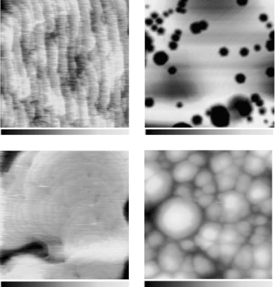
surface. This different behavior after chemical etching is shown in Fig. 12.2
for InN, where the +c and –c-polarity are in- and n-polarity, respectively.
CBED is a powerful method to detect polarity in sample, which works
in the transmission electron microscope (TEM) (Ponce et al., 1996). in the
measurement, the CBED pattern observed from the sample is compared
with the simulated CBED pattern by considering the lattice structure and
sample thickness as well. The CBED measurement is a unique method to
detect polarity at the atomic level, and demonstrates signicant advantages in
analyzing domain structures at the micro- to nano-scale. The disadvantage is
that the measurement is complicated and the sample preparation is also rather
difcult. The surface reconstruction revealed from RHEED has been widely
used to determine the polarity of iii-nitrides and Zno (smith et al., 1998).
This measurement can be taken in-situ in molecular beam epitaxy (MBE).
For example, the N-polar GaN surface shows the reconstruction of 1 ¥ 1, 3
¥ 3, 6 ¥ 6, and 6 ¥ 12 while that of Ga-polar shows the reconstruction of 2 ¥
2, 5 ¥ 5, 6 ¥ 4 and pseudo-1 ¥ 1. as for the aln, it has been suggested that the
reconstructions of 1 ¥ 1 and 2 ¥ 6 showed Al-polarity while that of 1 ¥ 1, 1 ¥
3, 3 ¥ 3, and 6 ¥ 6 indicated n-polarity (Lebedev et al., 1999). one problem
concerning this method is that it is difcult to nd surface reconstruction for
semiconductor layers since it requires rather at and metal-rich surfaces.
In-polarityN-polarity
0 [nm] 1.13
0 [nm] 6.88
As grown
0 [nm] 16.02
0 [nm] 157.26
Etched 13h
12.2 Atomic force microscopy images of as-grown and 13 h-etched
InN layers with different polarities. The scanned area for each image
is 1 ¥ 1 mm.
ThinFilm-Zexian-12.indd 290 7/1/11 9:44:14 AM
291Polarity controlled epitaxy of III-nitrides and ZnO
© Woodhead Publishing Limited, 2011
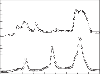
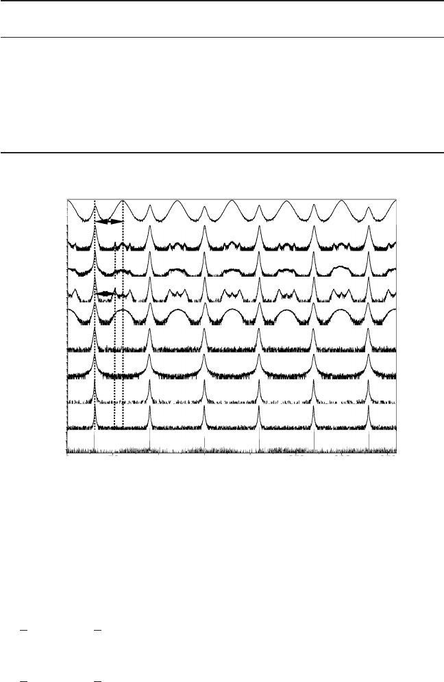
CaiCiss is a derivative of the generic technique of ion scattering
spectroscopy, in particular of low energy ion scattering spectroscopy. In
CAICISS measurement, a simple 180° backscattering geometry enables us
to determine the atomic positions at both an outermost surface and slightly
deeper layers.
CaiCiss spectra, including information on the surface structure
and lattice polarity, is obtained by analyzing the intensity of scattered signals
as a function of incident angle. The polarity is determined by comparing the
experimental CAICISS spectra to the simulated ones shown in Fig. 12.3, for
example in the case of InN. As shown in the gure, three peaks at 23°, 47°
and 72° are observed in simulated CAICISS spectra for +c-polarity while
six peaks at 15°, 23°, 32°, 51°, 67° and 74° are seen for –c-polarity.
CPGE is a newly reported method to detect the lattice polarity (Zhang
et al., 2009). In CPGE, a net current was generated without adding any
external bias under the irradiation of a circularly polarized light. The origin
of the CPgE can be attributed to the lack of spatial inversion symmetry.
The former degeneration band splits into two bands with opposite spin
indices as symmetry reduces. When the semiconductor layer is radiated by
circularly polarized light, an asymmetrical distribution of excited electrons
in momentum space is generated due to the optical selection rules, which
leads to a net current in the sample.
As a wurtzite semiconductor, III-nitrides and ZnO are lacking in inversion
symmetry. along the c-direction, the lattice of +c-polarity can be regarded
as a complete inversion of that of –c-polarity. Thus the spin-orbit interaction
in the samples with contrary polarities should be opposite, resulting in an
opposite spin splitting. Therefore, the sign of photocurrent due to CPgE
should be opposite for samples with different polarities because of the opposite
Signal intensity of ln (a.u.)
N-polarity
In-polarity
15
23
32
51
69
74
72
47
23
0 20 40 60 80
Incident angle q (deg)
12.3 Simulated CAICISS spectra of InN.
ThinFilm-Zexian-12.indd 291 7/1/11 9:44:15 AM

292 Thin film growth
© Woodhead Publishing Limited, 2011
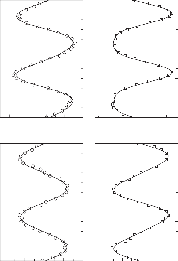
spin splitting. It has been conrmed by experimental observation that both
CPgE photocurrents and their dependences on the incident phase angle are
opposite for InN layers with different polarities, as shown in Fig. 12.4. It
is found that the above phenomenon is independent of the conduction type,
i.e. both n- and p-type InN shows the same sign of CPGE current and the
same dependence on the incident phase angle as well. Therefore, polarity can
be easily determined by investigating CPgE photocurrents in the measured
samples. It is worth noting that the CPGE measurement system is very easy
to construct at low cost and the measurement itself is also very simple and
non-destructive to samples. The disadvantage is that measurement is at the
macro-scale and it is very difcult to detect samples at the micro- or nano-
scale.
12.3 Polarity issues at heteroepitaxy and
homoepitaxy
although free-standing gan, aln and Zno substrates are commercially
available now, they are seldom used in epitaxy yet because they are several
tens to hundreds times more expensive than sapphire, which is the most popular
substrate up to now. It means that most epitaxy is heteroepitaxy. Sapphire
itself is non-polar along the c-direction. its atomic structure consists of an
al atom bilayer and an o single layer. Thus, it is very important to control
the surface of sapphire just in front of epitaxy. next, the effect of surface
treatment on rotation domains/polarity is shown, using as an example ZnO
epitaxy on sapphire by MBE.
Table 12.1 shows the surface treatment methods for sapphire substrate
before epitaxy of ZnO buffer layer, where etching, TC, H*, O*, Ga and N*
means chemical etching by a mixture of h
2
so
4
:h
3
Po
4
= 3:1 at 110°C, thermal
cleaning (TC) under ultra-high vacuum (UhV), atomic hydrogen treatment,
oxygen radical pre-treatment, ga atomic layer pre-deposition and nitridation
by using nitrogen radical, respectively (Yoshikawa et al., 2004). Figure
12.5 shows the XRD f-scans for (102) plane of ZnO epilayers grown with
the different sapphire surface pre-treatments listed in Table 12.1. The XRD
f-scan for (113) Al
2
o
3
is also shown for comparison. The dominant domain
in sample A is 30°-rotated compared to the ‘main’ domains observed in the
other samples B–I whose peaks are located at the same j angles as those
of (113) plane of Al
2
o
3
. These two domains have the epitaxy relationship
[112
0]ZnO//[1120]Al
2
o
3
and [1010]ZnO//[1120]Al
2
o
3
, respectively. The
latter is often called the main domain and the former is called the 30°-rotated
domain. There are three kinds of possible surface structures on clean sapphire:
terminated by o layer, single al layer, and al bi-layer. The oxygen layer is
sixfold symmetric while the Al layer is threefold symmetric. On the other
hand, both Zn and o are sixfold symmetric in Zno (the same is also true for
ThinFilm-Zexian-12.indd 292 7/1/11 9:44:15 AM
© Woodhead Publishing Limited, 2011
Photocurrent (nA)
8
4
0
–4
–8
0.8
0.4
0.0
–0.4
–0.8
0.8
0.4
0.0
–0.4
–0.8
8
4
0
–4
–8
0 60 120 180 240 300 360
(a)
0 60 120 180 240 300 360
(c)
0 60 120 180 240 300 360
(d)
0 60 120 180 240 300 360
(b)
n-type ln-polarity
n-type N-polarity
Quarter wave plate angle (deg)
p-type ln-polarity
p-type N-polarity
12.4 Photocurrents
observed in
four kinds of
InN layers with
different polarities
as a function of
quarter-wave
plate angle j.
Samples in (a)–(d)
are n-type In-
polarity, n-type
N-polarity, p-type
In-polarity and
p-type N-polarity,
respectively.
Incidence angles
are +25° in all
measurements.
ThinFilm-Zexian-12.indd 293 7/1/11 9:44:15 AM
294 Thin film growth
© Woodhead Publishing Limited, 2011
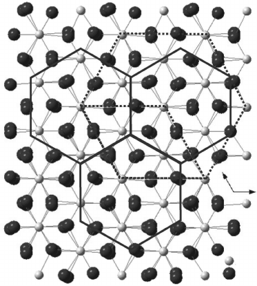
III-nitrides). The main domain is usually formed when the Zn atom forms
bonds with O atoms on the sapphire surface with epitaxial relationship of
[101
0]ZnO//[1120]Al
2
o
3
and lattice mismatch of about 18.2%, as shown in
Fig. 12.6. On the other hand, the 30° domain is formed due to the bonding
of O atoms in ZnO with Al atoms resulting in an epitaxial relationship of
[112
0]ZnO//[1120]Al
2
o
3
with a mismatch of about 31.8%. It is clear that
Intensity (logarithmic scale)
0 50 100 150 200 250 300 350
f–scan (deg)
30°
102
(113)
ZnO
Al
2
O
3
21.8°
A
b
C
d
E
f
G
h
I
12.5 XRd f-scans for (102) ZnO epilayers grown with several different
procedures of sapphire surface treatments. Three kinds of rotation
domains were observed after several surface treatments, but single
domain was obtained after Ga pre-exposure and sapphire nitridation.
XRd f-scan for (113) Al
2
O
3
is also shown here for comparison. The
surface pre-treatment conditions are shown in Table 12.1.
Table 12.1 The different pre-treatment methods of sapphire substrate before the
growth of ZnO buffer layer
Samples Etching time
(mins)
TC time
(mins)
h* time
(mins)
O* time
(mins)
Ga thickness
(ML)
N* time
(mins)
A 30
b 30 30
C 30 30 10
d 30 30 30
E 30 30 30 30
f 30 30 2
G 30 30 10 2
h 30 30 30 30 2
I 30 30 10 60
ML = monolayer.
ThinFilm-Zexian-12.indd 294 7/1/11 9:44:15 AM
295Polarity controlled epitaxy of III-nitrides and ZnO
© Woodhead Publishing Limited, 2011
the main domain is dominant in samples B–I in Fig. 12.5, though the 30°-
rotated domain is dominant in sample A. The third rotation domain, which
is 21.8°-rotated compared to the main domain, is observed in samples B,
C, and D, where it is stronger in longer H*-treated sample D. But if the
surface treatment for sample D is followed by O* pre-treatment, those peaks
become broad and nally the 21.8° domain cannot be identied though the
integrated intensity around both 21.8°- and 30° -rotated domains becomes
stronger. The 21.8°-rotated domain is most likely due to the Al-rich surface,
which has been conrmed by CAICISS and scanning force microscopy
(SFM) measurements (Barth and Reichling, 2001). The sapphire surface is
Al-rich after TC and it becomes Al-richer after H* pre-treatment due to the
loss of O atoms. Figure 12.5 shows that the intensity of the diffraction peak
of the 21.8° domain becomes stronger with increasing exposure period of
H*. It shows evidence that this rotation domain is ascribed to the Al layer
of sapphire. When ZnO buffer layer growth begins, O atoms form bonds
with Al atoms rst due to the Al-rich surface and relatively stronger bonds
of al–o in comparison to Zn–o. hence, the rotation domains of al layer
inuence the following ZnO layer and results in the 21.8° domain. On the
other hand, the surface is terminated at the O-plane after O* pre-treatment
and the Al metallic plane cannot be formed on the surface, which leads to
the elimination of the 21.8° domain as shown in Fig. 12.5.
a
Al + 3
O–2
12.6 Atomic structure of sapphire (perpendicular to c-axis) and
schematic illustration of the epitaxial relationship between ZnO and
sapphire. The dotted and solid lines show the bonding configurations
of two rotation domains, respectively.
b
ThinFilm-Zexian-12.indd 295 7/1/11 9:44:16 AM
296 Thin film growth
© Woodhead Publishing Limited, 2011
Ga pre-exposure on the O*-treated surface affects the ZnO epitaxy
dramatically as shown in Fig. 12.5, and the rotation domains were completely
suppressed resulting in a single domain, which is independent of treatment
condition, i.e., TC, TC+H* and TC+H*+O*. This is because Ga acts as the
template following ZnO layer deposition since it can migrate more easily
than the Al onto the surface and can uniformly cover it. When the growth
of the ZnO buffer layer begins, O atoms will bond with Ga atoms, resulting
in a single rotation domain. Furthermore, sapphire nitridation is also very
effective in eliminating the rotation domains as shown in Fig. 12.5. Following
sapphire nitridation, a very thin n-polarity aln layer is formed and this layer
acts as the template following ZnO layer growth. The AlN layer is a single
domain with hexagonal structure, which leads to the single domain ZnO.
In addition, the ZnO shows O-polairty on the Ga-treated surface while Zn-
polarity is formed on the nitrided sapphire surface. This will be discussed
in detail in section 12.6.
The important point to be emphasized here is that the samples with
multiple domains usually show mixed polarity and the treatment of surfaces
has great inuence on the epitaxy of ZnO and nitrides. Thus, it is important
to control the surface to eliminate the multiple domains and thus to be able
to control the polarity in heteroepitaxy.
The polarity control epitaxy on polar substrate is much easier than on
non-polar substrate. Due to the stronger bonds between metal atoms and N
or O atoms, the polarity usually follows that of the substrate. For example,
+c-polar nitride is grown on +c-polarity SiC while –c-polarity nitride is
obtained on –c-polaritysiC. in the case of homoepitaxy of iii-nitrides and
Zno, it is quite simple that the polarity usually remains the same during
epitaxy. The only exception happens when we do doping, for example,
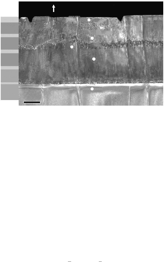
p-type doping of III-nitrides by using Mg as a dopant. Figure 12.7 shows the
TEM image and the polarity of inn layers. This multiple-inn layer structure
sample consists of four 390 nm thick InN layers grown at different [Mg]
levels, three 110 nm thick undoped spacer layers, a non-doped InN layer and
cap layer, respectively. [Mg]s in four Mg:InN layers from bottom to top are
1.0 ¥ 10
18
(1st layer), 5.6 ¥ 10
18
(2nd), 2.9 ¥ 10
19
(3rd) and 1.8 ¥ 10
20
cm
–3
(4th). It is shown that the polarity was inverted from In- to N-polarity above
the V-shaped domains, which happens at [Mg] ~ 2.9 ¥ 10
19
cm
–3
. Further
detailed investigation shows that the polarity inversion happens at [Mg] ~1
¥ 10
19
cm
–3
(Wang et al., 2007b). The observed N-polarity at position E in
Fig. 12.7 indicates that polarity inversion does not happen with further Mg
doping in the n-polarity case. investigation of the n-polarity sample does
not show any polarity inversion and thus this kind of polarity inversion only
happens in the in-polarity case. Very similar phenomena have also been
observed in gan (green et al., 2003).
ThinFilm-Zexian-12.indd 296 7/1/11 9:44:16 AM
297Polarity controlled epitaxy of III-nitrides and ZnO
© Woodhead Publishing Limited, 2011
12.4 Polarity controlled epitaxy of GaN and AlN
The most popular epitaxy methods for gan and aln are metal–organic vapor
phase epitaxy (MOVPE/also called MOCVD) and MBE. The polarity of
GaN and AlN can be controlled in both methods. In MOCVD growth, due
to the near quasi-equilibrium, the growth window to get +c-polar nitrides
is rather broad, while it is difcult to get –c-polar samples, in particular to
get a at surface for –c-polarity, since the growth window for –c-polarity
is rather narrow and the sample often includes +c-polarity domains, which
lead to rough surface with hexagonal grains with size up to hundreds of
micrometers. In MBE growth, it is relatively easy to control the polarity by
controlling the buffer layer growth.
If GaN is grown directly on sapphire substrate, it is mainly Ga-polarity,
which is due to the Al-rich surface of sapphire substrate after thermal cleaning
under UhV (Xu et al., 2002). However, sapphire nitridation is commonly
used in order to improve the crystal quality of GaN and/or AlN. During the
nitridation, n atoms replace o atoms and a thin aln or alno layer is formed
with an epitaxial relationship of [101
0]AlN//[1120]Al
2
o
3
(namkoong et al.,
2002). The nitridation temperature has a large effect on the properties of
the formed AlN thin layer and inuences the properties of the grown GaN.
Low temperature nitridation (200–400°C) is often used since the AlN layer
formed is much purer and includes less no. But this process usually takes
a much longer time than high temperature nitridation though the aln layer
formed by the lattice process often includes no in a higher atom ratio. as far
g = [0002]
Cap
Spacer
Spacer
buffer
GaN
Spacer
Mg:InN
(4th)
Mg:InN
(3rd)
Mg:InN
(2nd)
Mg:InN
(1st)
500 nm
A
E
d
C
b
Idbs
Ga-polarity
N-polarity
N-polarity
In-polarity
In-polarity
[Mg]:1.8 ¥ 10
20
cm
–3
[Mg]:2.9 ¥ 10
19
cm
–3
[Mg]:5.6 ¥ 10
18
cm
–3
[Mg]:1.0 ¥ 10
18
cm
–3
12.7 Cross-sectional dark field TEM images of a multiple-layer-
structure InN film recorded with g = [0002]. The sample structure is
shown on the left.
ThinFilm-Zexian-12.indd 297 7/1/11 9:44:16 AM