Czichos H., Saito T., Smith L.E. (Eds.) Handbook of Metrology and Testing
Подождите немного. Документ загружается.

498 Part C Materials Properties Measurement
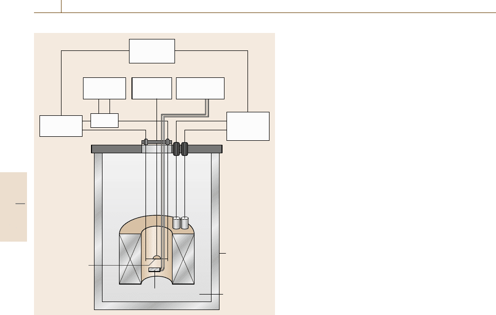
Computer
Voltmeter
Nano-
voltmeter
Temperature
controller
Magnet
power
supply
Current
source
Standard
resistor
Twisted-pair wires
Dewar
Cryogen bath
Sample
Thermometer
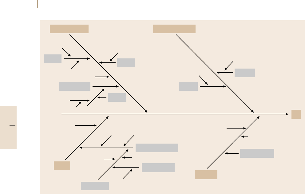
Fig. 9.17 Measurement setup for the characterization of super-
conductors (after [9.18]). The resistance of the superconductor
is determined by a voltage–current measurement. The apparatus
allows for the variation of temperature and magnetic field to de-
termine T
c
and B
c
vided into so-called type-I and type-II superconductors.
If a superconductor of type-I is kept at a temperature
T < T
c
and the magnetic induction B is increased there
is a critical magnetic induction B
c
, where the super-
conductor becomes normal conducting. Below this B
c
,
screening currents on the surface of the superconduc-
tor compensate the magnetic field inside. This means
that a type-I superconductor behaves like a perfect dia-
magnet, μ
r
=0[9.17]. Since this effect is also observed
for a volume surrounded by a superconductor, these
type-I superconductors allow perfect shields for mag-
netic fields at low temperatures.
Superconductors of type-II show a different behav-
ior. With increasing magnetic induction B, the transition
from the superconducting state to the normal con-
ducting state occurs continuously with two critical
inductions B
c1
and B
c2
.BelowB
c1
, a type-II supercon-
ductor behaves as one of type-I. At the critical induction
B
c1
, the magnetic field starts to penetrate the conduc-
tor creating flux vortices. At the critical induction B
c2
no more vortices can be created and the magnetic field
can completely penetrate the superconductor and it be-
comes normal conducting. The critical induction B
c2
is
typically much higher than B
c1
or the B
c
of a type-I
superconductor. Some properties (T
c
and B
c
)oftypical
superconductors are listed in Table 9.4.
The measurement of these parameters are carried
out in an apparatus allowing for control of both, tem-
perature and magnetic field by measuring the voltage
as a function of current through the superconductor
(Fig. 9.17)[9.18].
Similar to the determination of the DC conductivity
the voltage drop over a short length of a supercon-
ducting strand is measured, passing a DC current I.
At constant temperature T and magnetic induction B
the current I is varied to determine the critical current
density of the material under test. Other possible mea-
surements are the determination of T
c
as a function of
B or of B
c
as a function of T with I kept constant.
With these measurements it is possible to characterise
a superconductor. Standardized methods for the deter-
mination of parameters are described in [9.19].
9.3 Electrolytic Conductivity
The electrolytic conductivity is a measure of the amount
of charge transport of ions in solution. While in met-
als the current is carried by electrons in metals, in
electrolyte solutions, molten salts and ionic solids the
charge carriers are ions. The extent to which current
flows through an electrolyte solution depends on the
concentration, charge and mobility of the dissolved ions
present.
The SI derived unit of conductivity is siemens per
meter (S/m). The symbol for electrolytic conductivity
is κ in chemistry, σ or γ in solid-state physics. Very
low conductivity values are often expressed in terms of
resistivity (ρ =1/κ) in the unit ohm meter (Ω m).
9.3.1 Scale of Conductivity
Electrolytic conductivity is a nonspecific sum parame-
ter reflecting the concentration and mobility of all ions
dissolved in a solution. Since the mobility of the ions is
temperature dependent, the conductivity also depends on
Part C 9.3
Electrical Properties 9.3 Electrolytic Conductivity 499
High purity water
Deionized water
Rain water
Drinking water
Mineral water
Waster water
Process water
Hemodialysis
Seawater
1 mol/l HCl
0.055 µS/cm
1 µS/cm
50 µS/cm
100–1000 µS/cm
1–8 mS/cm
10–500 mS/cm
15 mS/cm
50 mS/cm
332 mS/cm
400–7000 µS/cm
0.05 µS/cm
0.1 µS/cm
10 µS/cm
10 mS/cm
100 mS/cm
1000 mS/cm
100 µS/cm
1 mS/cm
1 µS/cm
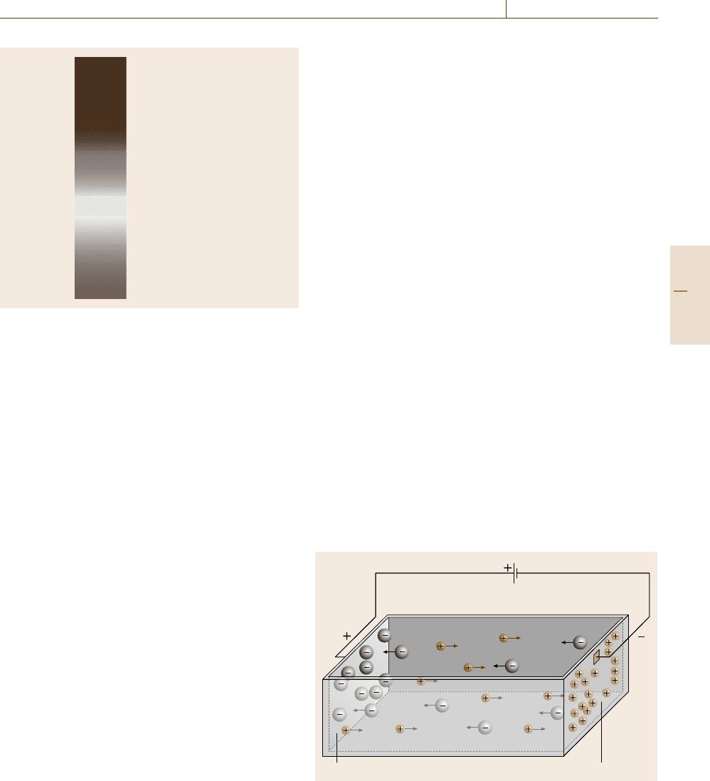
Fig. 9.18 The scale of conductivity with examples of vari-
ous aqueous solutions at 25
◦
C
temperature. Sometimes the term specific conductance
is used to describe conductivity. Since electrolytic con-
ductivity is nonspecific this expression is misleading and
should be avoided. Figure 9.18 shows the electrolytic
conductivity of different aqueous media at 25
◦
C.
The measurement of conductivity ranges from qual-
ity control of high purified water to waste water treat-
ment monitoring and process control in chemical in-
dustry. Electrolytic conductivity can also be used to
determine the relative ionic strength of solutions and as
a detection technique in ion chromatography.
Electrolytic conductivity is in fact the most widely
used parameter to monitor the overall ionic purity of wa-
ter and it is considered the major parameter defining and
ranking grades of purified water, e.g., in pharmaceutical,
semiconductor and power plant industries. Electrolytic
conductivitymeasurements are used for the evaluation of
water quality under regulations and standard practices,
e.g., drinking water and water used in food industry.
Important parameters in specific areas as, for instance,
the measurement of the amount of total dissolved solids
(TDS) and the salinity of sea water are also related
to conductivity measurements. Furthermore, electrolytic
conductivity is also measured in nonaqueous or mixed
solutions like fuels and paints and varnishes, respec-
tively for quality control purposes.
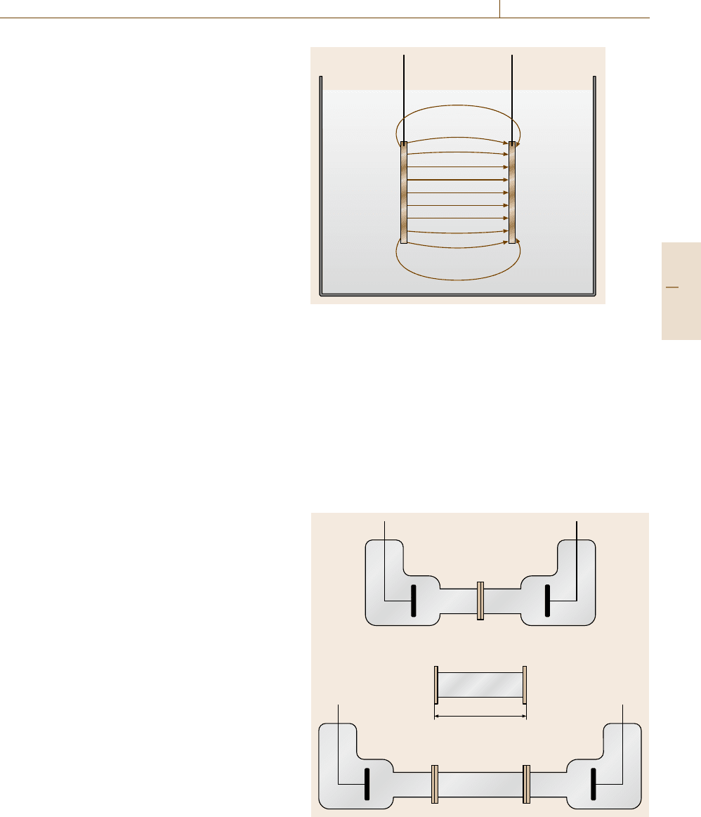
9.3.2 Basic Principles
In a volume, in which a homogeneous electric field is
present, the conductivity κ is given as the ratio of the
current density j, generated by the field, and by the
electric field strength E
κ E = j . (9.10)
Figure 9.19 schematically shows such a volume with
respect to an electrolyte solution. Two parallel elec-
trodes are immersed into the solution and connected to
a voltage source. The applied voltage generates a homo-
geneous electric field in the volume. Positive ions move
constantly towards the cathode, while the negative ions
move towards the anode.
Ion Mobility
For a volume of a constant cross sectional area A,
electrode distance l and with a homogeneous, constant
electric field of strength E, the voltage U across the
sample between the electrodes is given by
U =lE . (9.11)
The field exerts a force F on an ion of charge ze ac-
cording to (9.12), where z is the signed charge number
of the ion and e the elementary charge
F
z
= zeE . (9.12)
This force (9.12) accelerates the cations in the di-
rection of the cathode and anions towards the anode. An
ion moving through the solvent experiences also a fric-
tional force F
R
proportional to its velocity. Assuming
Stoke’s law of friction is applicable [9.20], the frictional
force is given by (9.13) and where r is the radius of
U
Anode Cathode
Fig. 9.19 Ions in solution conduct the electric current. The positive
ions (cations) constantly move towards the negative electrode (cath-
ode), while the negative ions (anions) move towards the positive
electrode (anode)
Part C 9.3
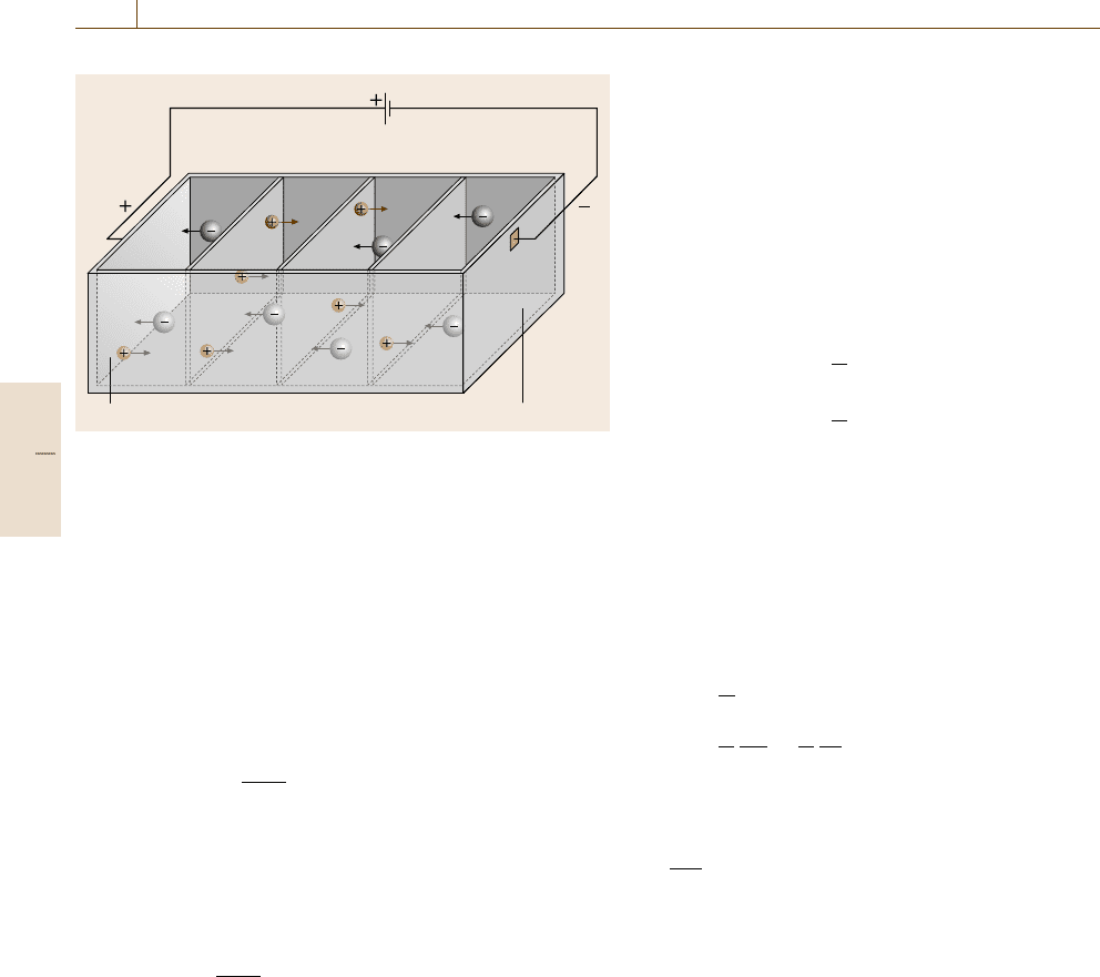
500 Part C Materials Properties Measurement
U
Anode Cathode
A
Fig. 9.20 The charge carried per time Δt period through the area A
results in the current I
+
and I
−
, respectively
the ion, which includes the radius of its solvate shell,
η is the viscosity of the solvent and w the speed of ion
motion
F
R
=6πrηw . (9.13)
The two forces act in opposite direction. After a short
time the speed of ion motion reaches a steady
state (9.14)and(9.15)
F
z
=−F
R
, (9.14)
w = E
ze
6πrη
. (9.15)
Note that the direction of the movement is determined
by the sign of z and that the speed of motion is pro-
portional to the field strength. From (9.15)afield
independent quantity for the speed of ions, the ion mo-
bility u
i
can be derived
u =
ze
6πrη
, (9.16)
with
w =uE . (9.17)
A strong electrolyte i. e. potassium chloride (KCl),
A
ν+
B
ν−
dissociates into ν
+
cations A and ν
−
an-
ions B carrying the charge z
+
e and z
−
e, respectively.
Lets assume the amount of substance concentration of
an electrolyte solution is c, then the concentration of
cations is ν
+
c and of anions is ν
−
c. The number of
cations and anions, respectively, per volume is ν
+
cN
A
and ν
−
cN
A
. N
A
is Avogadro’s constant. In the elec-
tric field, cations and anions move with speed w
+
and
w
−
in opposite direction. Hence, during a time period
Δt a positive charge of ΔQ
+
= N
A
ν
+
cz
+
ew
+
AΔt and
anegativechargeofΔQ
−
= N
A
ν
−
cz
−
ew
−
AΔt pass
an area A asshowninFig.9.20.
The charge carried per time period through the
area A results in the current I
+
= ΔQ
+
/Δt and
I
−
= ΔQ
−
/Δt, respectively [9.21]. Inserting Faraday
constant F (9.18) and using (9.15)and(9.11)givesI
+
(9.19)andI
−
(9.20) depending of the applied voltage U
F = N
A
e , (9.18)
I
+
= Fν
+
z
+
cu
+
A
l
U , (9.19)
I
−
= Fν
−
z
−
cu
−
A
l
U . (9.20)
According to (9.19)and(9.20) an electrolyte solution
shows the same electric behaviour as an ohmic resistor
R =ρ(A/l), where ρ is the resistivity of the conducting
material.
Molar Ionic Conductivity
With Ohm’s law (9.21), we find for the conductivity κ
+
(the reciprocal of resistivity) of the cations (9.22),
I =
U
R
, (9.21)
κ
+
=
l
A
1
R
+
=
l
A
I
+
U
. (9.22)
Inserting (9.19)into(9.22) yields (9.23) for the mo-
lar ionic conductivity λ
m+
of the cations.
κ
+
ν
+
c
= z
+
u
+
F = λ
m+
. (9.23)
The molar ionic condcutivity λ
m−
of the anions is de-
rived similarly.
Since the conductivity depends on concentration of
all mobile ions, measured values for different solutions
are not directly comparable. For this reson the molar
conductivity Λ
m
of electrolytes (9.24)asthesumof
the molar ionic conductivities of anions and cations has
been inroduced. Equations (9.23)and(9.24) applied to
the anions and cations in the solution yield (9.25). The
molar conductivity is expressed in S m
2
mol
−1
Λ
m
=ν
+
λ
m+
+ν
−
λ
m−
, (9.24)
κ =cΛ
m
. (9.25)
For strong electrolytes, Kohlrausch’s law empirically
relates the molar conductivity with concentration ac-
cording to (9.26) meaning that the molar conductivity
Part C 9.3
Electrical Properties 9.3 Electrolytic Conductivity 501
decreases with increasing concentration due to ionic
interaction
Λ
m
=Λ
0
m
−K
√
c , (9.26)
where λ
0
m
is the limiting molar conductivity of an elec-
trolyte at infinite dilution, K is a (typically small)
constant and depends primarily on the type of elec-
trolyte and on the solvent. In an aqueous solution the
ions arrange in a way that on a time average each ion
is surrounded by a sphere of counter ions. As a conse-
quence two main effects lead to a decrease of the molar
conductivity with increasing electrolytic concentration.
When the ions move in an applied electric field they per-
manently try to rebuild the ionic sphere, which results
in a restoring force and lowers their mobility. This ef-
fect is called the relaxation or asymmetry effect. The
so called electrophoretic effect is a result of the ionic
sphere influencing the friction force which a solvated
ion experiences when moving through the solution. For
a detailed description of the classical Debye–Hückel–
Onsager theory and further sophisticated quantitative
treatment of the concentration dependence of the con-
ductivity see [9.22, 23]. If the sample contains only the
species of interest and if the concentration dependence
of this species is known, conductivity measurement can
be used to estimate concentration.
Weak electrolytes dissociate only to a certain de-
gree, which depends on the concentration of the weak
electrolyte. Therefore the molar conductivity is mainly
determined by the nonlinear dependence of the dissoci-
ation constant α (9.27) on the electrolyte concentration
α =
Λ
m
Λ
0
m
. (9.27)
The limiting molar conductivity for any electrolyte so-
lution can be expressed in terms of the limiting molar
conductivities of the anions and cations (9.28). This re-
lation is known as Kohlrausch’s law of the independent
motion of ions in electrolyte solutions at infinite dilution
Λ
0
m
=ν
+
λ
0
m+
+ν
−
λ
0
m−
. (9.28)
Limiting conductivities of cations and anions in var-
ious solvents are listed in [9.23]. The ion mobilities
and therefore the limiting ionic molar conductivities of
the hydronium and of the hydroxyde ions are much
larger than for other ions due to a different trans-
port mechanism. Hydronium and hydroxyde ions are
not transported through the solution but protons are
transferred by a sequential von Grotthuss type proton-
hopping mechanism through water bridges [9.24].
9.3.3 The Measurement
of the Electrolytic Conductivity
Basic Measurement Principle
An equipment to measure the electrolytic conductivity
consists of a cell, mostly with built-in temperature probe
and a measurement device to determine the resistance
(and the temperature) of the cell (conductivity meter).
The conductivity cannot be measured directly. Accord-
ingto(9.22) the conductivity κ = κ
+
+κ
−
of a solution
under investigation is evaluated from the measurement
of the resistance R of a sample in the cell and the
geometric cell dimensions. In case of two parallel elec-
trodes opposite to each other the geometric parameters
in (9.22) are combined in terms of the cell constant K
(9.29).
K =
l
A
. (9.29)
K is equal to 1.0cm
−1
if the current flow contained
within 1 cm
3
of sample solution is between the two elec-
trodes of 1 cm
2
area and in a distance of 1 cm. The
so-called standard cell is shown in Fig. 9.21.
The cells shown in Figs. 9.19 and 9.21 are ide-
alized. In practice, side effects must be taken into
account. These effects in particular include effects at the
electrode–solution interface: electrode polarisation, i. e.
accumulation of ions at the electrodes (so-called double
layer capacitance), charge transfer across the electrodes
(polarization resistance) and adsorption/desorption phe-
nomena. Additionally, fringing electric fields at the
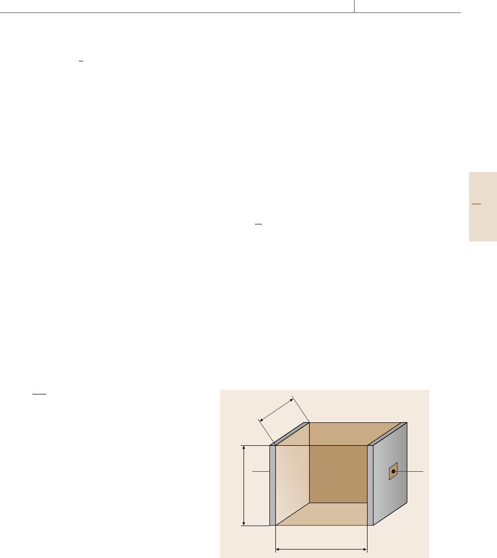
1cm
1cm
1cm
Fig. 9.21 For a standard cell, the volume of the sample
solution is the area of the electrode times the distance be-
tween the electrodes
Part C 9.3
502 Part C Materials Properties Measurement
Resistance R Temperature T
Resistance
Calibration
Capacitance
Frequency
Polarization
Cable
Design
Area
Contamination Electrodes
Meter
Sensor
Calibration
Range
Reference temperature
Cell design
T-coefficient
T-coefficient
Reference solution
Concentration
Viscosity
Composition
Geometry
Certificate
CO
2
CO
2
K
cell
K
cell
, primary
Sample
κ
Fig. 9.22 The relevant uncertainty sources and their relationship are shown in a cause and effect diagram (fishbone)
cell margin and the geometric capacitance of the two
electrodes affect the measured resistance. The solu-
tion resistance is therefore typically determined from
impedance measurements Z
i
( f
i
) at various frequencies
f
i
rather than a DC measure-ment of U and I. Depend-
ing on the electrode design, electrode effects affect the
measured impedance spectrum at low frequencies, typi-
cally up to a few kHz, while the influence of the (rather
small) geometric capacitance shows up at frequencies
in the upper kHz range. The resistance R of the solution
therefore can be derived from an extrapolation (9.30)
of the real part of the impedances measured in the low
frequency range [9.25]
R = lim
(1/ f )→0
Re{Z
i
( f
i
)}. (9.30)
Furthermore, the cell design must be optimized to
permit minimization the influence of fringing electrical
fields. For this purposes a confinement of the current
path to a defined volume having a large cross section A,
and a small electrode distance is desirable. On the other
hand this reduces the measured resistance. This is of
disadvantage for the conductivity measurement of solu-
tions having large conductivities, since the uncertainty
of resistance measurements increases for resistances in
the ohm and milliohm region. Hence, geometric and
electric properties of a conductivity cell are typically
optimised for a conductivity range of interest.
If the cell constant K is determined from the ge-
ometric dimensions of the cell and if the resistance is
measured traceable back to the SI, such as outlined
above, the resulting conductivity of a solution is trace-
able to the SI unit S m
−1
.Suchprimary cells are used to
measure the conductivity of primary reference solutions
(primary standards). Aqueous solutions of potassium
chloride are usually used for this purpose. In a traceabil-
ity chain, the known electrolytic conductivity of primary
standard is used to calibrate conductivity cells of un-
known cell constant. These cells are then used together
with properly calibrated conductivity meters for routine
measurements the results of which are traceable to the
SI unit S m
−1
[9.26]. Calibration and measurements of
such devises are usually performed at a single frequency.
On a worldwide scale the equivalence of the existing na-
tional primary measurement standards are ensured by
means of international comparison measurements.
Part C 9.3
Electrical Properties 9.3 Electrolytic Conductivity 503
The best way to obtain all information on possi-
ble sources of uncertainty on the resulting conductiv-
ity of the sample is a cause and effect diagram shown
in Fig. 9.22. This fishbone visualizes the relationship of
the uncertainty sources. The main sources of uncertainty
are the measurement of the resistance of the sample, the
sample temperature, the cell constant and the stability of
the sample.
Temperature Influence
on Electrolytic Conductivity
The conductivity of a solution depends on temperature.
Consequently, only conductivity values obtained at the
same measurement temperature can be compared. The
concept of reference temperatures (mostly 25
◦
C) was
introduced to solve this problem. A temperature correc-
tion function allows the conductivity meter to convert
the actually measured conductivity to that of the refer-
ence temperature.
There are three ways to deal with the temperature:
dependence of conductivity
•
No correction (according to the specification of the
United States Pharmacopeia (USP)[9.27]) for wa-
ter used in pharmaceutical industry, like water for
injection (WFI);
•
Linear correction to a reference temperature, which
is, depending on the target uncertainty, appropriate
for small deviations of up to 1
◦
C;
•
Nonlinear correction (e.g. for natural waters accord-
ing to ISO 7888 [9.28]).
The standard uncertainty of the temperature should be
u = 0.1 K or better. For low target uncertainty it is rec-
ommended to thermostat the sample so that the same
temperature is used for calibration and measurement.
Primary Cells
The conductivity of primary reference solutions are
measured by means of conductivity cells with cell
constants, which are determined by geometric mea-
surements. Various cell types have been tested in the
past on their ability to avoid or minimize fringe ef-
fects and stray fields typical for two-electrode cells as
seen from Fig. 9.22. Two common models are shown in
Figs. 9.23 and 9.24.
The cell type schematically shown in Fig. 9.24 was
developed at the National Institute of Standards and
Technology (NIST, Gaithersburg) [9.29]. The so-called
Jones cell [9.30] is based on the principle of a ge-
ometrically measured, removable center section. The
cell constant is primarily determined by the cross sec-
Fig. 9.23 Fringe effects occur on the edge of a two-
electrode cell. If the field is not homogeneous it is not
possible to determine the cell constant by a geometrical ap-
proach
tional area and length Δl of the glass tube separating
the platinum electrodes rather than by the size of the
electrodes themselves. In this primary cell the resistance
of the solution can be reduced by removing the cen-
ter section. The difference in the measured resistances
is therefore correlated to the length of the removable
center section. The conductivity of the sample can
Δl
Fig. 9.24 Jones-type primary cell with removable center section
Part C 9.3
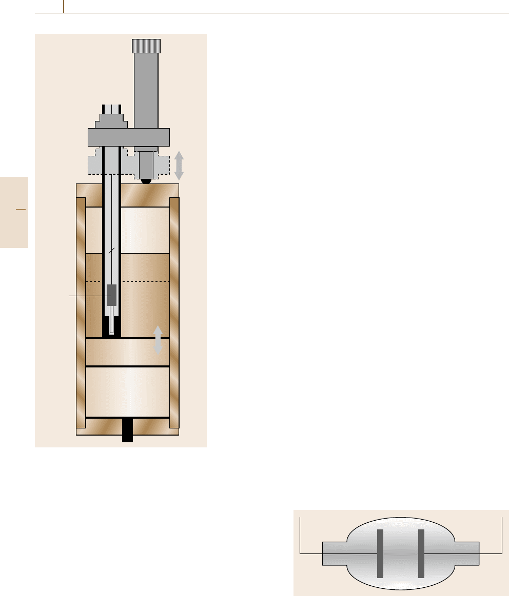
504 Part C Materials Properties Measurement
Pt 100
Δl
Δl
Fig. 9.25
Primary differ-
ential cell with
adjustable elec-
trode distance
therefore be determined from Δl and the differential
resistance.
The disadvantage of this cell design is that the
cell must be disassembled and cleaned between mea-
surements with and without the center section which
enhances the risk of contamination. The relatively ex-
panded uncertainty (coverage factor k = 2) e.g. for the
conductivity of a 0.01 mol/kg potassium chloride so-
lution with nominal conductivity of 1.41 mS/cm (at
25
◦
C) is of the order of 0.03%.
A different approach of a two-electrode cell with
well-known geometry developed at the Physikalisch-
Technische Bundesanstalt (PTB, Braunschweig) [9.31]
goes back to Saulnier [9.32,33]. In this design one elec-
trode is mounted on a movable piston. The distance
between the two electrodes can be adjusted very pre-
cisely without the cell being disassembled. The cell
design is shown in Fig. 9.25. The cross-sectional area
is constant and is determined by the internal diameter
of the cylindrical tube. The two electrodes are made
of Pt, directly vapour deposited onto the electrode bod-
ies [9.34]. If the spacing between the two electrodes is
large enough, the distribution of the electric field in the
bulk solution is not influenced by the movement. There-
fore the difference in the measured resistances then can
be attributed to the change Δl of the distance between
the electrodes, so that conductivity can be calculated
from the differential values, quite similar to the Jones
cell.
Four-Terminal DC Cell
Conductivity measurements of a primary reference so-
lution can also be performed using a four-electrode
DC cell [9.35]. This method can be applied at higher
conductivities, i. e. at low resistances. It has the advan-
tage [9.26] to avoid the reactive effects typical of AC
circuits. Measurements are effected by two outer Pt cur-
rent electrodes, which imprint a constant current to cell,
and two inner electrodes to measure the voltage drop
across a portion of the cell. The current has to be kept
relatively low to avoid heating the solution and elec-
trolysis. Reversible potential electrodes are required to
eliminate any polarization effect. The traceable value of
the cell constant is directly determined through the ge-
ometry of a center glass tube precisely bored at which
ends the potential electrodes are located.
Commercial Conductivity Cells –
Two-Electrode Cell
The two-electrode cell as shown in Fig. 9.26 is the
classical conductivity cell sometimes called Kohlrausch
cell.
The two-electrode cell consists of two parallel elec-
trodes immersed in the sample solution. An AC current
Fig. 9.26 Classical two-electrode conductivity cell
Part C 9.3
Electrical Properties 9.3 Electrolytic Conductivity 505
at a single frequency is typically applied and the re-
sulting voltage is measured. Stray field and polarization
effects influence the measurement. These effects must
be kept under control in order to measure only the bulk
resistance of the sample. Polarization is a side effect of
the contact of electronically conducting electrodes with
a solution showing ionic conduction. A charge buildup
occurs at the electrical double layer at the electrode–
solution interface and causes a voltage drop across the
electrode surface. As a consequence, the measurements
can, in general, not be performed with DC but have to be
carried out with AC in the frequency range of typically
up to 5 kHz.
The deposition of a platinum black layer on
a platinum electrode (platinization) also reduces the
polarization effect by increasing the electrode sur-
face [9.36]. This increases the double layer capacitance
so that the measured impedance is virtually resistive.
It is important to choose the right frequency for the
respective application, which significantly depends on
the cell design and the solution under investigation. In
general, low frequencies in the sub-kHz region can be
applied at low conductivities. In this range the polar-
ization is negligible compared to the bulk resistance of
the sample. Frequencies in the low kHz region must be
applied at high conductivities in order to minimize the
influence of electrode polarization.
A disadvantage of the two-electrode cells is that any
changes of the electrode surface such as corrosion or
coatings influence the measurement result. If the elec-
trodes are covered by platinum black any scratch or
other damage would change the surface and therefore
the cell constant.
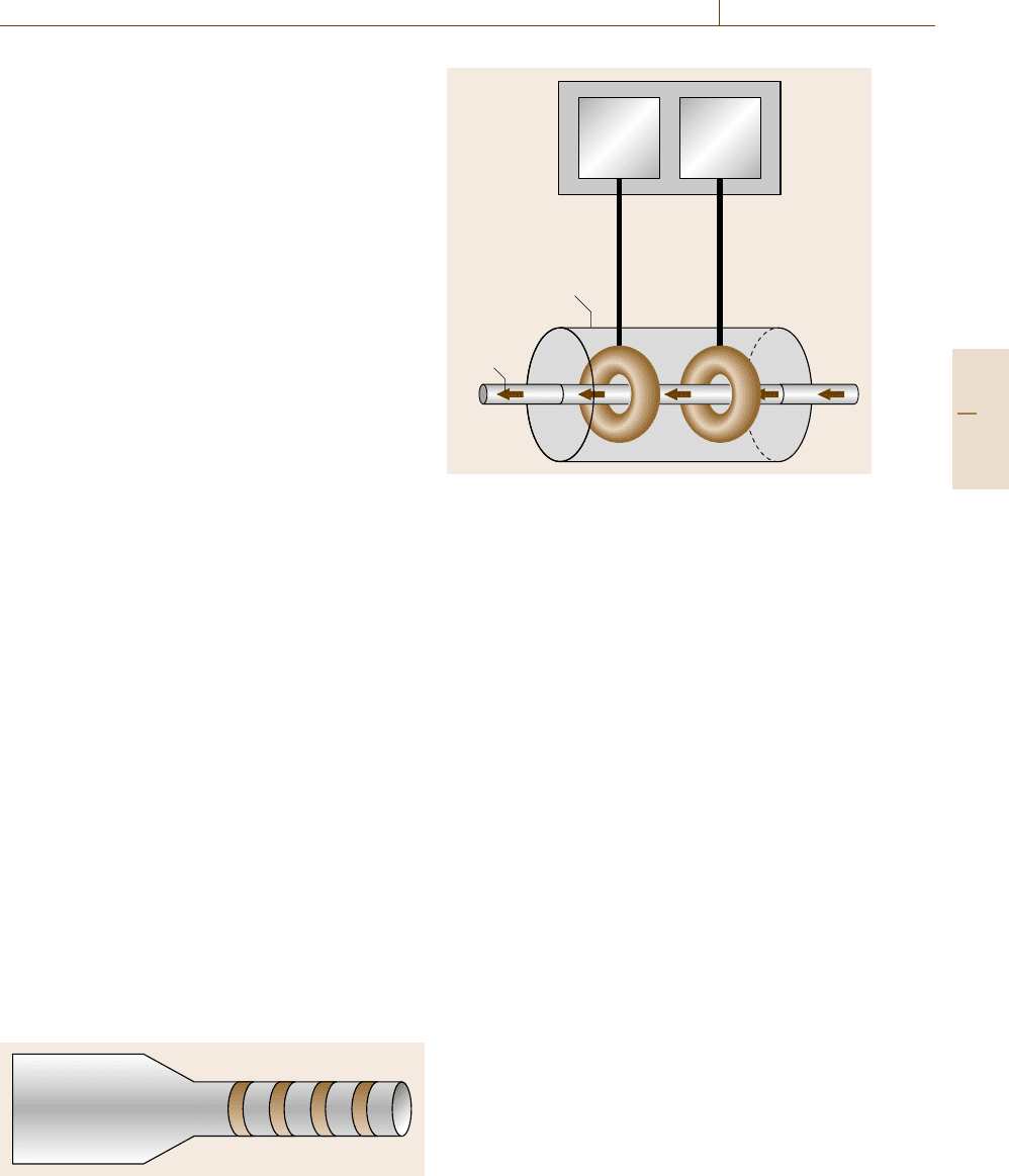
Four-Electrode Cell
The four-electrode cell reduces the problem of polar-
ization effects. Changes of the electrode surface like
blocking and coating do not influence the measurement
result. A typical four-electrode cell as oversimplified
shown in Fig. 9.27 consists of four concentric rings. One
outer pair of current electrodes and one inner pair of
voltage electrodes. A constant AC current is applied
to the outer pair of rings. The voltage is measured on
Fig. 9.27 Oversimplified four-electrode cell
Oscillator Detector
Cell cube
Sample
Fig. 9.28 Toroidal inductive conductivity cell
the inner rings with a large input impedance of the
impedance meter to reduce polarization effects.
Three-Electrode Cells
The three-electrode cell type is nowadays almost com-
pletely replaced by the four-electrode cell. In a three-
pole cell a third pole is connected to one electrode of
a two electrode cell, which serves to guide the electrical
field. In this way the stray-field can be reduced [9.37].
Electrodeless Conductivity Measurements –
Toroidal Inductive Conductivity
In a toroidal conductivity measurement cell as shown
in Fig. 9.28, the electrodes are located outside the so-
lution being investigated. An oscillating potential is
applied to the first electrode, which induces a cur-
rent in the solution. Inversely the induced current is
measured with the second toroidal coil [9.38]. A main
field of application is the process control, e.g., in food
industry.
Monitoring the Purity of Water
Since electrolytic conductivity is a sensitive measure
for the amount of ions dissolved in the solution,
a threshold for conductivity is a clear and simple
specification for the quality and purity of water in
general but also for high-purity water. The relevant
measuring range is below 0.1mS/m(0.06–1 μS/cm
at 25
◦
C). The US Pharmacopoeia [9.27]aswellas
the European one [9.39] have specified the standard
Part C 9.3
506 Part C Materials Properties Measurement
D
A
D
I
l
Fig. 9.29 Flow-through cell for the low conductivity
range. For this closed cell type the influence of air-borne
contaminations like carbon dioxide on the measurement
result can be avoided
for purified water, highly purified water and water
for injection for the pharmaceutical industry based on
conductivity measurements. Sectors that also use con-
ductivity thresholds for water purity are electrical power
plants, food industry, electronic industry and analytical
laboratories.
In the sub-mS/m region no certified aqueous refer-
ence solutions are available, because the conductivity
of aqueous solutions is not stable due to the influence
of atmospheric carbon dioxide (CO
2
). CO
2
dissolves in
water and partly forms carbonic acid. By that it con-
tributes to the measured conductivity value in the order
of 0.1mS/m, depending on the partial CO
2
pressure
present during the measurement. To compensate for the
D
A2
l
2
l
1
D
I2
D
A1
D
I1
Pt 100
Pt 100
Fig. 9.30 Primary flow-through cell for in-line conduc-
tivity measurements in the high-purity water range. The
concentric cell consists of two inner electrodes of differ-
ent length and one outer electrode. The gap between the
inner electrodes is filled with inert material
absence of certified reference solutions, a calibration
method based on high-purity water as a standard has be-
come widely accepted by the users of low conductivity
measuring devices [9.40]. For this purpose it is neces-
sary to determine the conductivity of high-purity water
traceable to the SI unit S/m.
Flow-Through Cell
for the Low-Conductivity Range
The most common cell design for in-line applications in
the high-purity water range is shown in Fig. 9.29. The
Part C 9.3

Electrical Properties 9.4 Semiconductors 507
concentric design minimizes electromagnetic interfer-
ence [9.41] and is suitable for integration of the cell into
a closed loop. Contamination with atmospheric carbon
dioxide from surrounding air is avoided for this type of
cell. For calibration it is integrated into a closed loop of
purified water together with a reference cell of known
cell constant, which is used to measure the conductiv-
ity of the purified water. In this way the purified water
in the loop is used as a transient reference material to
calibrate the commercial cell in-line and at the same
temperature.
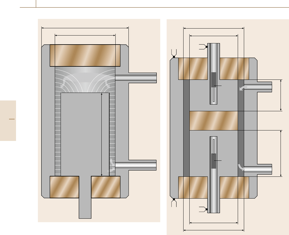
The principle of a primary reference flow-through
cell [9.42] is shown in Fig. 9.30. It consists of two in-
ner cylindrical electrodes of different lengths l
1
and l
2
and an concentric outer electrode, which herby form
two conductivity measurement cells. The gap between
the inner electrodes is filled with inert, nonconduct-
ing material. Platinum resistance temperature sensors
are mounted in each inner electrode. The cell con-
stant of each cell can be calculated from the inner
and outer diameter D
i
and D
o
, respectively, and from
the lengths of the inner electrodes according to (9.31).
Fringe effects at the holes and at the end of the elec-
trodes are considered in terms of an effective stray
length a
K
1
=
ln
(
D
o
/D
i
)
2π(l
1
+a)
,
K
2
=
ln
(
D
o
/D
i
)
2π(l
2
+a)
. (9.31)
Since the two cells just defer in length, a can be as-
sumed equal for both cells. Using κ = K
1
/R
1
= K
2
/R
2
(9.22) the effective stray length can be calculated from
the measured resistances R
1
and R
2
of the pure wa-
ter in the two cells. The cell constants are of the order
of 1 m
−1
with a relative expanded target uncertainty
(k =2) smaller than 0.5%. Because cell dimensions, re-
sistance and temperature measurements are measured
traceable to the SI unit, the conductivity of the high-
purity water can thus be determined in the SI unit S/m.
Another promising design of a primary flow-
through cell is based on the on the so-called van der
Pauw principle which is used extensively in solid-state
physics to measure surface resistivity. The principle is
based on a theorem similar to that of Lambert used for
the determination of the capacitance unit. The theorem
can be applied to a cell with constant cross section and
with four electrodes at the edges [9.43].
9.4 Semiconductors
Semiconductor materials offer a wide range of con-
ductivity according to their free carrier concentration,
starting from the intrinsic conductivity (10
−8
S/cm) up
to 10
5
S/cm by controlling the doping concentration
from 10
12
up to 10
21
cm
−3
. Thus, the determination of
the conductivity, conductivity type (n- or p-doped), and
the related majority carrier mobility are the most impor-
tant characterizations, especially in the case of newly
developed materials.
After these majority carrier properties are known,
minority carrier properties come into consideration,
which are mainly related to lattice defects (vacancies
and interstitials), but also to chemical impurities, which
produce (deep) electron or hole states within the band
gap. The most important parameter is the minority
carrier lifetime which is applied to describe leakage cur-
rents of p-n junctions, charge storage times in dynamic
memory cells or sensitivity of charge-coupled device
light sensors.
With respect to high-speed devices, like e.g. bipolar
transistors or photodiodes, saturated drift velocity val-
ues are needed to estimate the high-speed performance.
Many semiconductor devices reach their operating lim-
its with respect to some breakdown mechanisms, like
the onset of tunneling currents or impact ionization.
Table 9.5 gives a selected list on semiconductor
properties and related methods to determine their val-
ues. The following paragraphs give some guidance to
determine the most relevant parameters useful for de-
vice simulation, device design, and device analyses.
As all semiconductor devices need a more or less
ideal contacting of their active regions via metallization
of ohmic contacts, the final section collects measure-
ments methods for specific contact resistances.
9.4.1 Conductivity Measurements
Conductivity measurements on semiconductors are pre-
dominantly related to bulk material, e.g. semiconductor
wafers and epitaxial layers or layer stacks. The conduc-
tivity σ (S/cm) is related to the specific resistance ρ
(Ω cm)
σ =
1
ρ
.
(9.32)
Part C 9.4