Czichos H., Saito T., Smith L.E. (Eds.) Handbook of Metrology and Testing
Подождите немного. Документ загружается.

508 Part C Materials Properties Measurement
Table 9.5 Overview on selected semiconductor properties and related characterization methods
Property Symbol Characterization method
Specific resistance ρ Four-point probe,
van der Pauw method
Conductivity type (n- or p-type) Thermoprobe, Hall effect
Carrier concentration n, p Hall effect,
capacitance–voltage (C–V )
Carrier mobility μ
n
, μ
p
Hall effect with resistivity
Compensation ratio N
A
/N
D
, N
D
/N
A
Temperature dependence
of Hall coefficient
In-depth doping profile N(x) Capacitance–voltage (C–V ),
Hall effect with selective layer removal,
spreading resistance on beveled samples
Diffusion length L
n
, L
p
Junction photocurrent,
electron beam induced currents (EBIC)
Saturated drift velocities v
n,sat
, v
p,sat
I–V analysis (Kelvin method)
Ionization rates by electrons α
n
, α
h
Temperature resolved I–V
or holes (impact ionization) analyses
Minority carrier lifetime τ
n
, τ
p
I–V analysis, photoconductivity
Deep states (traps): density, N
t
Deep level transient
thermal emission rates, capture e
n
, e
p
, σ
n
, σ
p
spectroscopy (DLTS)
cross sections, energy level E
t
The conductivity can be calculated from basic semi-
conductor properties in case of dominating electron
conduction
σ =qμn , (9.33)
with the elementary charge q (1.602 × 10
−19
As), the
carrier mobility μ (unit cm
2
/(V s)), and the carrier den-
sity n (unit cm
−3
).
If both carrier types (electrons and holes) are con-
cerned, the conductivity is deduced from
σ =qμ
n
n +qμ
p
p . (9.34)
The standard method for measuring the specific resis-
tance of bulk materials and thin layers is the four-point
probe [9.44]. This method is well established for sili-
con and germanium but works as well on GaAs, InP,
and other III–V compound materials. By applying the
method to beveled surfaces, in-depth resistivity profiles
can be deduced (spreading resistance method [9.45]).
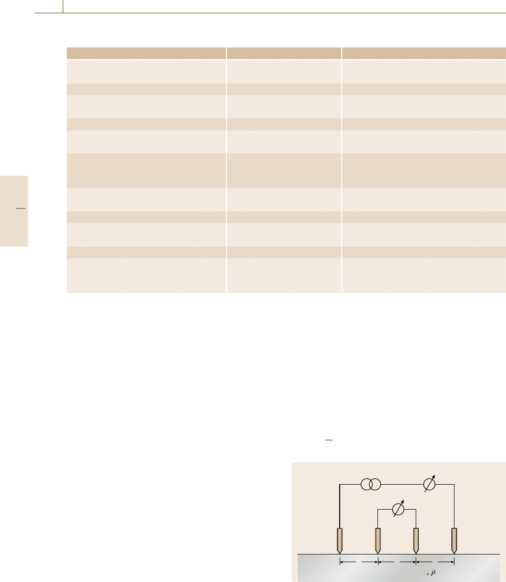
The basic measurement setup of the four-point
probe (c.f. e.g. DIN Norm 50431) is depicted in
Fig. 9.31. A measurement head comprising four spring-
loaded needles with equal distances s (e.g. s =1 mm), is
pressed onto the semiconductor sample with a pressure
ensuring good near-ohmic contacts, but soft enough not
to produce visible damage. The measurement current I
is fed via the outer needles through the sample. The
voltage V is measured between the inner needles. As-
suming a constant current source with nearly infinite
source impedance and a voltage meter with nearly in-
finite input resistance, possible contact voltages at the
needles due to the current flow can be neglected in this
Kelvin-like setup. The specific resistance of the sample
is
ρ =
V
I
c , (9.35)
I =const.
I
V
sss
Semiconductor wafer,
Fig. 9.31 Four-point probe on a semiinfinite semiconduc-
tor wafer with specific resistance ρ
Part C 9.4
Electrical Properties 9.4 Semiconductors 509
with c denoting a geometry dependent correction fac-
tor, depending on the sample dimensions and the needle
distances. The following constraints have to be fulfilled
in all sample configurations for accurate measurement
within inaccuracies below 1%
a) nearly ohmic contacts between the needles and the
semiconductor,
b) negligible heating of the sample due to the measure-
ment current I (mA range),
c) no excess injection of carriers, which would lead to
excess conduction (dark measurement),
d) no extreme surface potential induced surface band
bendings; otherwise leading to stronger surface ac-
cumulation or surface inversion layers which would
affect the bulk conduction.
In the following sections the correction factor c is given
for different samples geometries.
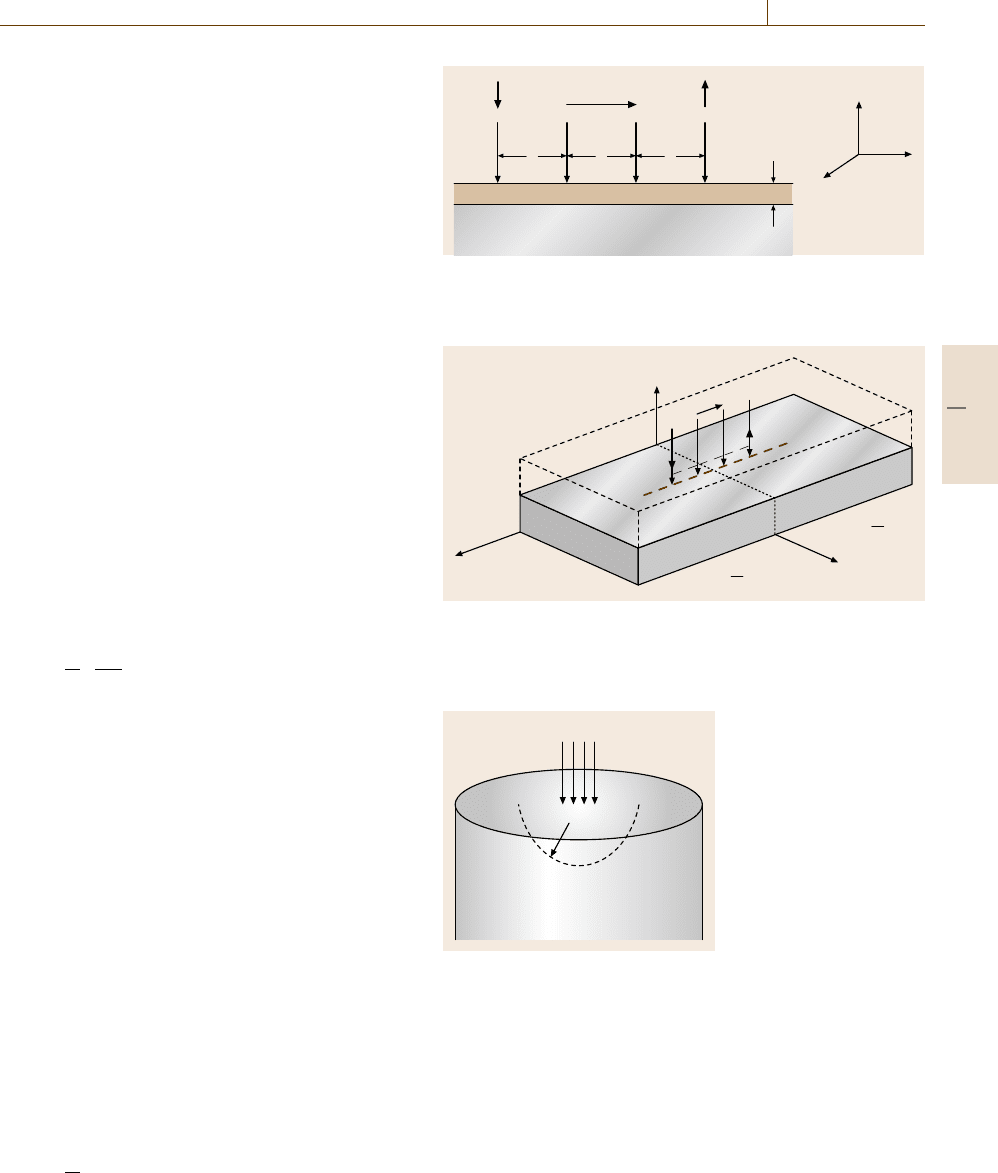
Conductivity of Thin Layer Samples
The measurement setup of the four-point probe applied
to a laterally infinitely extended thin layer of thickness
d and specific resistance ρ, grown on a semiinsulating
wafer is depicted in Fig. 9.32. The specific resistance
(unit Ω cm) of the layer can be deduced from the meas-
ured voltage V, induced by the current I using
ρ =
V
I
d
π
ln 2
. (9.36)
An error in the evaluation of the specific resistance ap-
proaches 1%, if the layer thickness d would be one
half of the needle distance s. This error would increase
to 8%, if the layer thickness d would equal the nee-
dle distance s. Normally, needle distances of 1 mm are
used, thus, for layer thickness values in the 1–10 μm
range this systematic error can be neglected easily. This
solution is also applicable in all cases, where the lat-
eral dimensions of the sample are much larger than the
threefold measurement–tip distance. If the latter con-
dition cannot be met a setup as in Fig. 9.33 hastobe
used.
Conductivity of Semiinfinite Bulk Samples
The measurement setup of the four-point probe applied
to a semiinfinitely extended bulk sample with a specific
resistance ρ, is depicted in Fig. 9.34. The specific resis-
tance of the semiinfinite bulk sample can be deduced
from the measured inner voltage V induced by the outer
current I by
ρ =
V
I
s2π. (9.37)
Semiinsulating substrate
1234
sss
II
V
d
z
x
y
ρ
Fig. 9.32 Four-point probe applied to a thin, infinitely extended
layer of thickness d and specific resistance ρ; the measured layer
is isolated by a semiinsulating substrate
z
b
d
l=
a
2
l=
a
2
x
s
s
s
y
V
I
I
Fig. 9.33 Four-point probe on a thin, rectangular shaped layer of
dimensions a× b×d with a specific resistance ρ; the measured layer
may be isolated by an underlying semiinsulating substrate or a pn-
isolation
IIVV
sss
d
Fig. 9.34 Four-point
probe on a semi-infinitely
extended bulk sample
with a specific resistance
ρ; the radius of the meas-
ured volume is defined
roughly by d > 3.5s
This is valid under the assumption, that the radius of
the measurement volume d > 3.5 s, with s denoting the
equal spaces s of the needle setup.
Conductivity
of Rectangular Shaped Small Samples
In some cases, the samples to be characterized exhibit
neither the shape of a semiinfinitely extended bulk sam-
ple nor the structure of a laterally infinitely extended thin
Part C 9.4
510 Part C Materials Properties Measurement
layer. Thus, a further solution is given for the case of
a rectangular shaped sample of finite dimensions a and
b(Fig.9.33).
The solution of this problem can be obtained by sev-
eral approaches, like finite difference methods. Here, an
analytical approach of Hansen [9.46] may be mentioned
which can be easily implemented on desktop comput-
ers. The Laplace equation is solved using a separation
of variables and applying standard boundary conditions
on the doubled sample (see dotted lines in Fig. 9.33)
without changing the field and current line conditions
in the original sample. A series expansion is developed
in [9.46] to deduce the specific resistance ρ from meas-
ured I–V values and the sample geometry data a, b,and
d as well as the probe head tip distances s
ρ =
V
I
s
bd
+
8
bd
×
∞
m=0
∞
n=0
cosh β
(
l −3s/2
)
sinh
(
βs/2
)
1 +δ
0,m
1 +δ
0,n
β cosh (βl)
−1
(9.38)
with (m, n) unequal to (0, 0) and
β =
2π
b
m
2
+
nb
2d
2
1/2
(9.39)
and δ
r,s
= Kronecker’s delta (δ
0,m
=1(m =0) or 0 (m >
0)).
A general remark for all four-point probe configu-
rations: the four-point probe can be applied to silicon
and germanium using pressures of the needles of ap-
proximately up to 50 p; in case of more sensitive III–V
materials like InP, the pressure of the probe needles has
to be reduced to around 5 p.
Conductivity of Isotype 2-Layer Stacks
If there are two adjacent layers (1, 2) with isotype
conduction type with individual sheet carrier concen-
trations n
1,2
(unit cm
−2
) and mobilities μ
1,2
(unit
cm
2
/V s), contributing to the total sheet conductance δ
s
,
the resulting mixed conductance in terms of the effec-
tive sheet carrier densitiy n
s
and effective mobility μ
s
can be calculated from the conductances of the single
layers according to [9.47]
n
s
=
(μ
1
n
1
+μ
2
n
2
)
2
μ
1
2
n
1
+μ
2
2
n
2
, (9.40)
μ
s
=
μ
1
2
n
1
+μ
2
2
n
2
μ
1
n
1
+μ
2
n
2
. (9.41)
It is assumed that the adjacent isotype layers are grown
either on a semiinsulating buffer layer or together being
isolated by a pn-junction from the substrate. Thus, the
substrate or buffer conductance should be negligible in
this two-layer mixed conduction model.
9.4.2 Mobility Measurements
The mobility μ of the majority carriers is extracted
by a two-step procedure applying van der Pauw test
structures [9.48]. Firstly, the specific resistance ρ is
measured, secondly the carrier concentration n is de-
termined. Both measurement setups use the same test
structure but apply different schemes for contacting to
feed the measurement current into the sample and to
measure the resulting voltages. In a final step the mobil-
ity is deduced from the equation σ =qμn solved for μ
μ =
σ
qn
=
1
qnρ
. (9.42)
The term |1/(qn)| is the Hall constant, which is indica-
tive of the carrier concentration n within the test sample.
Thus, the mobility can also be written as
μ =
R
H
ρ
= R
H
σ. (9.43)
Due to the fact that the Hall effect is polarity sensi-
tive with respect to the conduction type, the sign of the
Hall constant comprises the information of the dominat-
ing carrier type: negative sign – n-type, positive sign –
p-type. In the following, the Hall effect is explained in
more detail and some van der Pauw test structures will
be discussed.
Hall Effect, van der Pauw Structures
The Hall effect after Hall (1879) denotes the onset of
a voltage V
H
at a long thin sample of length a, where
a current I is driven through the long axis and a mag-
netic field B is applied perpendicular to the sample
(Fig. 9.35). Due to the balance of the Lorentz force
F =qv × B and the electric field force due to E
H
of the
Hall voltage, the Hall voltage for an n-type sample can
be deduced after integrating over the transverse field E
H
V
H
=−
1
nq
1
d
IB . (9.44)
The term −1/(nq) is known as the Hall constant R
H
of the sample, the sign of which depends on the carrier
type. In case of a p-type sample, the Hall constant has
a positive sign.
Thus, the Hall effect can be used to determine the
dominant carrier or conduction type of an unknown
semiconductor sample.
Part C 9.4
Electrical Properties 9.4 Semiconductors 511
The Hall voltage of either type can be written as
V
H
= R
H
1
d
IB , (9.45)
with voltage signs +/−↔p/n-type conduction.
When Hall’s constant R
H
is determined, the carrier
concentration can be deduced
n, p =
1
qR
H
(9.46)
(with n, p due to a negative, positive sign, respectively)
In principle, the mobility value can now be calcu-
lated from (9.43) assuming that the conductivity of the
sample was determined by the four-point probe before.
This method applying two different test samples would
work but it is rather unpractical. A more convenient way
was published in [9.48], where a disk of arbitrary shape
can be used for both types of measurement. In practice,
later a rectangular sample is preferred. The original van
der Pauw sample type is shown in Fig. 9.36; the sample
must not contain any holes. The van der Pauw sample is
used in two measurement configurations
1. For the measurement of the specific resistance.
The current I is fed into contacts M, N and the
voltage V is taken at contacts P, O. This I–V con-
figuration can be cycled around 90
◦
, and the voltage
at M, P taken, too. Thus, two resistances are built:
R
MN,OP
and R
NO,PM
.In[9.48], it is shown by a con-
formal mapping method that the sample’s specific
resistance obeys van der Pauw’s equation
e
[
−
(
πd/ρ
)
R
MN,OP
]
+ e
[
−
(
πd/ρ
)
R
NO,PM
]
=1 . (9.47)
The specific resistance can be solved from (9.47)
graphically or numerically, e.g. by a Newton
method. For the practically preferred rectangular
sample geometry the specific resistance can be de-
duced from
ρ =
πd
ln 2
R
MN,OP
. (9.48)
In this symmetrical case, the I–V configuration
can be rotated four times by 90
◦
and the resulting
four voltage values can be averaged. Addition-
ally, the current polarity can be reversed and the
resulting voltages averaged again. Thus small asym-
metries of the sample can be averaged by taking the
mean value of eight measurements. More elaborate
evaluation procedures in cases of asymmetric I–V
measurements in the van der Pauw configuration are
givenin[9.44].
2. For measurement of the carrier concentration.
For the determination of the carrier concentration
B
E
I
d
b
z
y
x
a
b
–q
E
y
E
H
V
H
I
Θ
Fig. 9.35 Hall effect at a long sample with dimensions a × b ×d,
where a measurement current I is driven along a, and a magnetic
field is applied perpendicular to a, b in z-direction
P
O
N
M
d
ρ
Fig. 9.36 van der Pauw
test sample of specific
resistance ρ, disc of arbi-
trary shape of thickness
d with infinitesimal small
contacts M, N, O, P at its
periphery
from a Hall measurement at the van der Pauw sam-
ple, the I–V setup is modified in which the current
and voltage contacts are now crossed. The Hall
constant is determined in this case by forming the
average out of two measurements
R
H
=
d
B
R
NP,OM
+R
OM,PN
2
. (9.49)
This scheme can also be improved by averaging
over eight Hall resistance terms, as given in [9.44].
The carrier mobility is now deduced using (9.43),
(9.49) together with (9.48).
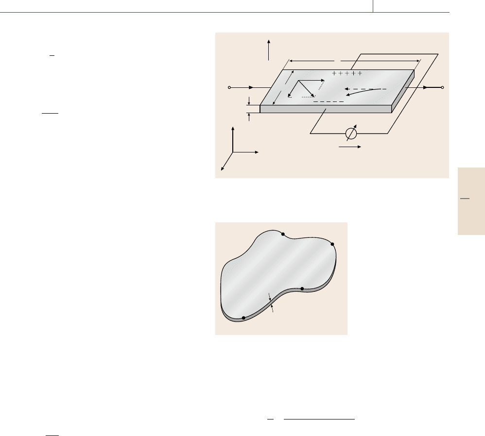
Van der Pauw Test Structures
It was mentioned before, that a rectangular test sam-
ple with quite small contacts at the corners can be
used favorably for the van der Pauw measurements
(Fig. 9.37). The ideal infinitesimally small contacts can
be approached by soldering 500 μm Sn balls into the
corners of the sample while using sample sizes of, e.g.
> 5×5mm
2
.
Part C 9.4
512 Part C Materials Properties Measurement
P
O
N
M
ρ
Fig. 9.37 Quadratic van
der Pauw test sample
with ideal infinitesimally
small contacts in the four
corners
a) b) c) d) e)
Fig. 9.38a–e van der Pauw test samples with nonideal finite con-
tact sizes (after [9.44])
However, real samples suffer from different nonide-
alities of the sample preparation; the contacts are not
small enough compared to the sample’s edge length
or the contacts are not correctly deposited at the sam-
ple’s corners. Respective correction terms can be found
in [9.44]. To overcome the distorting effects of finitely
extended contacts, a lot of alternative test samples are
in use. Figure 9.38 gives an overview of common van
der Pauw test sample geometries [9.44]. Very popular
is the clover-leaf structure (e), which can be fabricated
by ultrasonic cutting and which does not need further
electrical corrections even in the presence of finite con-
tacts. Very precise results can also be obtained from the
greek cross structure (b). Many discussions concerning
ease of fabrication, fragility, heat dissipation, and needs
of correction factors can be found in [9.44].
Temperature Dependent Carrier Concentration
and Compensation
The carrier concentration determined by the standard
Hall technique described so far is assumed to repre-
sent the value of the dopant concentration as well. This
is valid when a complete dopant ionization can be as-
sumed. In practice, at least two additional aspects have
to be considered.
Temperature Dependent Carrier Concentration
(Dopant Ionization < 100%)
The mobile carrier concentration n(p) follows the
dopant concentration N
D
(N
A
) up to concentration val-
ues of the order of the effective density of states (N
c
or N
v
, for n- or p-type conduction, respectively). The
effective density of states depends, besides the sam-
ple temperature (∝ T
3/2
), on the effective mass of the
carrier, e.g. for the conduction band E
c
N
c
=2
2πm
0
m
e
k
B
T
h
2
3/2
, (9.50)
with m
0
denoting the free electron mass and m
e
the
effective mass of the electrons; the other constants
have their usual meanings. Normally, electron effective
masses m
e
are smaller than hole effective masses m
h
.
Thus, the density of states in the conduction band is
smaller than in the valance band (for a first very rough
orientation take N
c
=10
18
cm
−3
and N
v
=10
19
cm
−3
for E
c
and E
v
, respectively). The free carrier concen-
tration n is regulated by the position of the Fermi level
E
F
with respect to the band edges E
c
and E
v
. Although
the Fermi distribution [9.49] gives the correct Fermi
level and carrier concentration, often Boltzmann’s ap-
proximation is used for nondegenerate semiconductors
(E
c
−E
F
> 3k
B
T), again denoted for the electron con-
centration: n = N
c
exp[−(E
c
−E
F
)/(k
B
T)] (for holes:
p = N
v
exp[(E
v
−E
F
)/(k
B
T)]). The Fermi level E
F
adjusts itself in relation to the band edges to pro-
vide overall charge neutrality for the sum of fixed
and mobile charges, i. e. for the charge sum of ion-
ized impurities and electron and hole densities (for the
n-type semiconductor: N
+
D
=n − p). The ionized im-
purity concentration N
+
D
is given by the Fermi level
position with respect to the impurity level energy E
D
N
+
D
= N
D
1
1 +g exp[−(E
D
−E
F
)/(k
B
T)]
(9.51)
with g denoting the ground-state degeneracy of the
donor level (g = 2(4) for electrons (holes)), E
D
usually
is some (ten) meV below the conduction band edge en-
ergy. This equation shows that complete ionization can
be achieved at Fermi level positions well below E
D
,i.e.
for doping concentrations below the effective density
of states N
c
. The charge neutrality equation together
with Boltzmann’s approximations for the free carrier
concentrations and the before mentioned ionization re-
lation for the dopant N
D
fixes the Fermi energy and
the free carrier concentrations for a given temperature.
For incompletely ionized donors, i. e. for lower temper-
atures (below 100 K) the carrier freeze-out range begins.
This means that only a certain percentage of the donor
concentration results in free electrons in the conduction
band. Thus, also the Hall technique will measure a re-
duced carrier density towards decreasing temperatures.
Fitting the free carrier concentration given by the above
Part C 9.4
Electrical Properties 9.4 Semiconductors 513
equations to a temperature-resolved Hall measurement,
e.g. within a range from 77 up to 400 K, allows the
determination of the dopant ionization energy E
D
.
Compensation Effects
In semiconductors there may also coexist a smaller
amount of the adverse dopant type of opposite charge
polarity besides the dominating one which determines
the sign of the Hall constant and the conduction type (n-
or p-type). This adverse dopant type tends to partially
compensate the effectiveness of the major dopant and
results in a pronounced temperature behavior of the free
charge concentration in excess of that of an uncompen-
sated semiconductor. At normal (room) temperatures,
the free carrier concentration is given by n = N
D
−N
A
,
while at reduced temperatures, the free carrier concen-
tration diminishes much more pronounced due to the
compensation and incomplete ionization of the major-
ity carrier dopant type. The charge neutrality equation
is now replaced by N
+
D
−N
−
A
=n − p. Applying again
Boltzmann’s approximations for the free carrier concen-
trations and the noted ionization relation for the dopants
N
D
and N
A
, the free electron concentration in case of
a partially compensated n-type semiconductor can be
deduced
n
N
D
=−
1
2
n
1
gN
D
+
N
A
N
D
+
1
4
n
1
gN
D
+
N
A
N
D
2
+
1
g
1 −
N
A
N
D
n
1
N
D
,
(9.52)
with n
1
= N
c
exp[−(E
c
−E
D
)/(k
B
T)]. This equation
can be related again to a temperature-resolved Hall mea-
surement n(T ). The fit allows to determine, besides the
donor ionization energy E
D
, also the compensation ra-
tio N
A
/N
D
. In dominating p-type semiconductors, the
compensation ratio is defined as N
D
/N
A
(< 1).
In all cases of compensated semiconductors, the
Hall mobility is more or less lower than in the uncom-
pensated cases because the additional ionized impurity
scattering effects at the compensating centers lead to re-
duced mobility values. This effect can be even more
pronounced at low temperatures when carrier scatter-
ing effects by lattice vibrations are negligible, i. e. when
the Hall mobility is only affected by free carrier or ion-
ized impurity scattering. Thus, the maximum mobility
values of low-doped semiconductors achievable at e.g.
77 K give invaluable information on the purity of the
material.
Hall Mobility and Drift Mobility
Deducing from the Hall effect, the carrier velocity was
orientated solely along the y-direction of the constant
current fed through the long test sample. In practice, the
electrons (or holes) are moving not with a linear trans-
lation but they are moving on cycloid-type paths due to
the two forces of the electric field in y-direction and to
Lorentz’s force in x-direction. These cycloid-type curves
are interrupted by scattering events of the carriers at lat-
tice vibrations and (ionized) impurities depending on
the impurity density. A result of these combined move-
ments of the carriers in x-andy-directions under the
combined electrical (E
y
) and magnetic (Hall) field (E
H
)
forces are trajectories, where the carriers feel the crys-
tallographic properties of the semiconductor crystal in
both directions x and y. Consequently, the Hall mobil-
ities μ
Hn,p
may deviate from the drift mobilities μ
n,p
.
The newly introduced Hall factor r
H,n
denotes the ratio
of μ
H,n
/μ
n
; in the case of a p-type semiconductor, r
H,p
denotes the ratio of μ
H,p
/μ
p
. The Hall factor modifies
the formerly Hall constants for an n-type semiconductor
R
H,n
=−r
H,n
1/(qn) and for the p-type semiconductor
R
H,p
=−r
H,p
1/(qp). The Hall factors depend slightly
on the magnetic field, the crystal structure, and the mea-
surement temperature. For high magnetic fields, the Hall
factor tends to unity. In practice, due to often unknown
precise values of the Hall factors, a unity value is as-
sumed for material quality comparisons of different epi-
taxial approaches or annealing conditions.
Field-Effect Mobility (FET Transistor)
In devices like field-effect transistors (FET), the con-
ducting channel is controlled by gate electrode applying
an electrical field perpendicular to the current path.
The channel can be either located at the surface
of the device, like in a MISFET (metal-insulator-
semiconductor FET) or the channel may be buried,
like in HFET/HEMT (hetero structure/high-electron
mobility FET) transistors. For these large variety of de-
vices, the Hall effect can be applied to measure the
channel mobility which can be either enhanced by two-
dimensional electron gas effects or be reduced due to
surface scattering effects between the insulating gate
oxide and the surface conducting channel, compared to
bulk conduction in thicker epitaxial layers.
9.4.3 Dopant and Carrier Concentration
Measurements
The measurement of the dopant and carrier concen-
tration is mainly done by capacitance–voltage (C–V )
Part C 9.4
514 Part C Materials Properties Measurement
analyses because this method delivers not only aver-
aged carrier concentrations but provides the in-depth
carrier concentration profiles, too. Capacitance–voltage
(C–V) analyses are predominantly executed applying
LCR-meters, which can measure the sample’s AC con-
ductance besides the capacitance. C–V analyses should
be evaluated under the assumption that the loss tangent
(G/ωC) of the sample does not exceed some percent
proving that the capacitance for a given measurement
frequency is dominating the conductance contribution.
If sufficiently low values of the loss tangent cannot be
achieved for a standard frequency of e.g. 1 MHz, then
higher frequencies should be chosen in case of paral-
lel conductance leakage, or lower frequencies should be
used in cases of high series resistances of the samples
under test. A rule of thumb is to choose the measure-
ment frequency according to the minimum of the loss
tangent. If stray capacitances in parallel to the sample
are present, then those should be determined by apply-
ing adequate test structures and subtracting them before
conducting further C–V analyses.
The C–V method can be most simply explained
applying a Schottky contact, i. e., a metal contact on
an n-type semiconductor. Firstly, the doping profile
analysis is explained under the assumption of the de-
pletion approximation. Secondly, some limitations of
the C–V method with respect to in-depth resolution
limitations due to Debye length effects are discussed.
Thirdly, correction procedures are explained for the
most important cases of near-surface doping profiles
in metal–insulator–semiconductor (MIS) structures and
in-depth implantation profiles as well as high-low dop-
ing profiles.
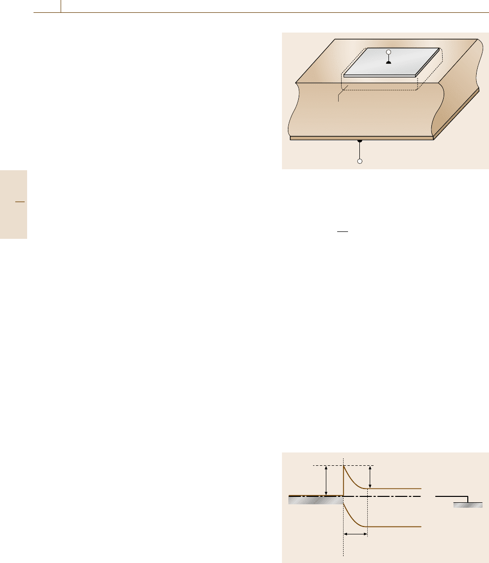
Capacitance–Voltage (C–V)Analyses
The basic capacitance-voltage (C–V) evaluation with
respect to semiconductor in-depth doping profiling is
based on the depletion approximation, i. e. on the as-
sumption of an abrupt space charge edge in conjunction
with complete dopant ionization. A suitable sample
test structure is shown in Fig. 9.39. A Schottky contact
metal with defined area A is evaporated on top of the
semiconductor, while ohmic metallization is provided
at the back side. Due to the work function difference of
the metal to the electron affinity of the semiconductor,
a space charge region of depth w is formed. The depth
of the space charge region can be controlled by a re-
verse biased voltage applied to the top gate electrode.
Within the depletion approximation, the capacitance of
the space charge region (neglecting side wall effects and
other stray capacitances) is given by the plate capacitor
Metal
Area A
Space charge region w
n-type semiconductor (ε
r
)
Ohmic back contact
Fig. 9.39 Schottky metal contact (area A) on top of an n-
type semiconductor with space charge region depth w
model
C
sc
=ε
0
ε
r
A
w
0
, (9.53)
with ε
r
being the dielectric constant of the semiconduc-
tor, ε
0
the vacuum permittivity, and w
0
the space charge
width at zero bias. Figure 9.40 shows the related band
diagram at zero bias. The Schottky barrier height Φ
Bn
induces a band bending within the semiconductor of
qV
bi
, with V
bi
being the built-in voltage of the Schot-
tky diode. E
c
, E
v
and E
F
are the conduction, valence
band edges, and the Fermi level, respectively. The Fermi
level at equilibrium is constant throughout the whole
metal–semiconductor structure indicating the absence
of current flow at zero bias conditions. If an external
reverse voltage is applied to the left-sided metal elec-
trode, the band bending of the semiconductor increases
and the width of the space charge region increases, too.
Consequently, the resulting capacitance is reduced, ac-
cording to (9.53). The depletion approximation model
can be seen in Fig. 9.41, where the in-depth free electron
Metal
n-type semiconductor (ε
r
)
E
c
E
F
E
V
w
0
qV
biΦ
Bn
Fig. 9.40 Band diagram of a metal–semiconductor Schott-
ky contact in thermal equilibrium at zero bias
Part C 9.4
Electrical Properties 9.4 Semiconductors 515
Concentration
Depth
Neutral
region
Space
charge
region
N
D
(w)
N(w)Δw
n(x)=N
D
(w)
L
D
Δw
w
n(x)=0
0
Fig. 9.41 Arbitrary in-depth doping profile N
D
(w)andre-
sulting in-depth free electron concentration profile n(x),
described according to the depletion approximation
concentration n(x) is shown in idealized form compared
to an arbitrarily assumed in-depth doping concentra-
tion profile N
D
(w). In the neutral region, the free
carriers (here electrons) compensate the ionized donor
atoms [N
+
D
(w) = N
D
(w) =n(x)]. Depletion approxima-
tion means that the free carrier concentration at the
edge of the space charge region makes an abrupt tran-
sition down towards zero concentration inside the space
charge region. This corresponds to a zero Debye length.
The Debye length L
D
=
ε
0
ε
r
k
B
T/(q
2
n) denotes a typ-
ical screening length depending on the square root of
temperature T compensating space charge distortions
from thermal equilibrium of the carrier concentration n.
By solving Poisson’s equation div D = ρ and in-
tegrating twice over the space charge region, the
total band bending potential V depending on the
space charge region depth w, can be deduced:
V =
1
2
qN
D
w
2
/(ε
0
ε
r
) (so far a constant dopant profile
N
D
is assumed). By combining this equation with the
plate capacitor equation, solving for an expression of
1/C
2
(V) and differentiating 1/C
2
(V ) versus the exter-
nal voltage, an expression for a nonconstant in-depth
carrier concentration profile n(x) (identified equal to
N
D
(x)) due to the depletion approximation can be found
N
D
(x) =
1
qε
0
ε
r
1
A
2
C
3
(V)
dC(V)/dV
for an n-type semiconductor, (9.54)
N
A
(x) =−
1
qε
0
ε
r
1
A
2
C
3
(V )
dC(V)/dV
for a p-type semiconductor.
(9.55)
In both cases, the depth x is calculated from the plate
capacitor model x = ε
0
ε
r
A/C(V).
The accuracy of the C–V method is mainly deter-
mined by the known accuracy of the gate electrode area,
e.g. an accuracy of the area A within 1% gives an ac-
curacy of the doping profile of 2%. Further, the spatial
variation of the doping profile should be small within
a Debye length to assure the validity of local charge
neutrality during in-depth profiling.
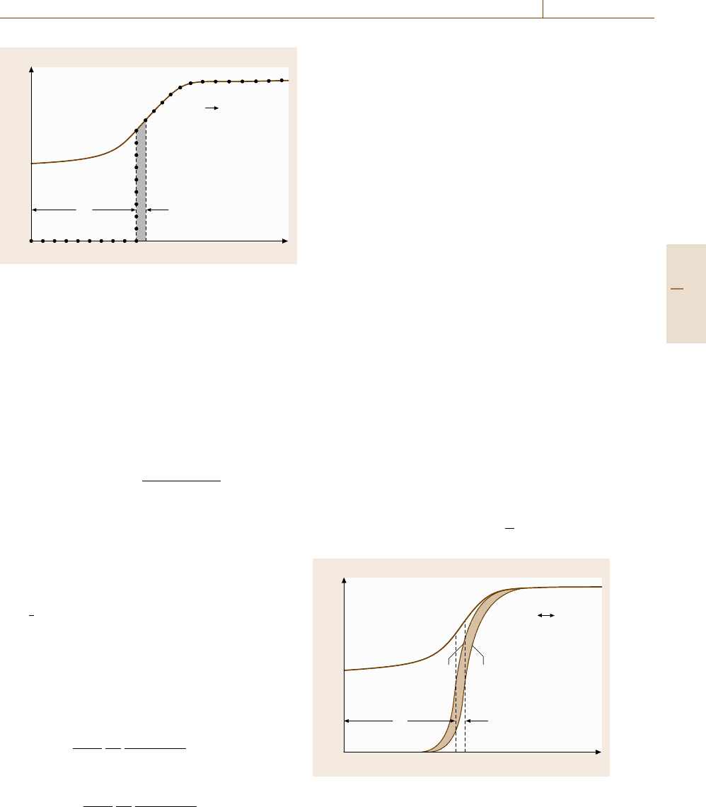
Limitations on C–V Analyses,
Applying the Depletion Approximation
The in-depth resolution of doping profiles determined
by the C–V profiling method is limited by the Debye
length. The finite Debye length leads to a smear out of
the abrupt space charge edge over roughly 2–3 Debye
lengths. This phenomenon is shown in Fig. 9.42. Two ef-
fects may result: first, in the case of abrupt steps within
the doping profile, the equilibrium carrier profile will not
follow the doping step with the same abruptness (local
neutrality is not fulfilled); second, in the case of near-
surface profiling, the free carrier tail of the space charge
edge will touch the interface region even if a certain
space charge region is still opened. In both cases profil-
ing errors will arise. In the first case, the abruptness of
real doping profiles cannot be measured adequately; in
the second case the apparent carrier profile (from which
the user concludes the doping profile) will increase artifi-
cially towards the interface when the space charge region
is smaller than about two Debye lengths.
The Debye length can be reduced by lowering the
measurement temperature (L
D
∼
√
T), but for very low
Concentration
Depth
Neutral
region
Space
charge
region
N
D
(x)
n
2
(x)
n
1
(x)
n(x) ≈ N
D
(x)
L
D
Δw
w
Fig. 9.42 Arbitrary in-depth doping profile N
D
(x)and
more realistic in-depth free electron concentration profile
n(x) in presence of Debey length smearing of the space
charge edge
Part C 9.4
516 Part C Materials Properties Measurement
temperatures, the dopant ionization is diminished, too.
Thus, the measured carrier concentration would under-
estimate the true dopant concentration and this approach
was limited to very shallow donor levels.
These further aspects of finite Debye length prob-
lems during doping profiling will be discussed in the next
section.
Debye Length Corrections for Near-Surface
Doping Profiles in MOS/MIS Structures
and for Ion-Implanted In-Depth Profiles
In this section two correction procedures will be de-
scribed which help to improve approximations of the
true doping profiles while the apparent C–V (carrier)
profiles are affected by Debye length broadening ef-
fects.
Near-Surface Doping Profiles in MOS Structures
MOS (metal–oxide–semiconductor) or MIS (metal–
insulator–semiconductor) structures play an important
role in all CMOS based devices, like CMOS transistors
or (B)CCD ((buried) charge-coupled device) focal plane
arrays. The surface doping profile, i. e. the doping pro-
file in the direct vicinity of the dielectric–semiconductor
interface needs to be known very accurately because
the value and homogeneity of the threshold voltage
depends on it. MIS structures isolate quite well any
current flow due to the high specific resistivity of the
dielectric/oxide. This allows to solve Poisson’s equa-
tion while neglecting any current flow and to consider
the additional contribution of mobile carriers in the
space charge region [9.50]. By applying this analyti-
cal approach Ziegler et al. [9.50] extended the range
of the depletion approximation till up to the flatband
point of MIS capacitors which means up to the semi-
conductor surface. They developed an analytic tabular
correction algorithm for the apparent carrier profile,
which is calculated from the depletion approximation
and they avoid any artificial increase of the apparent
carrier profile towards the surface, even when the profil-
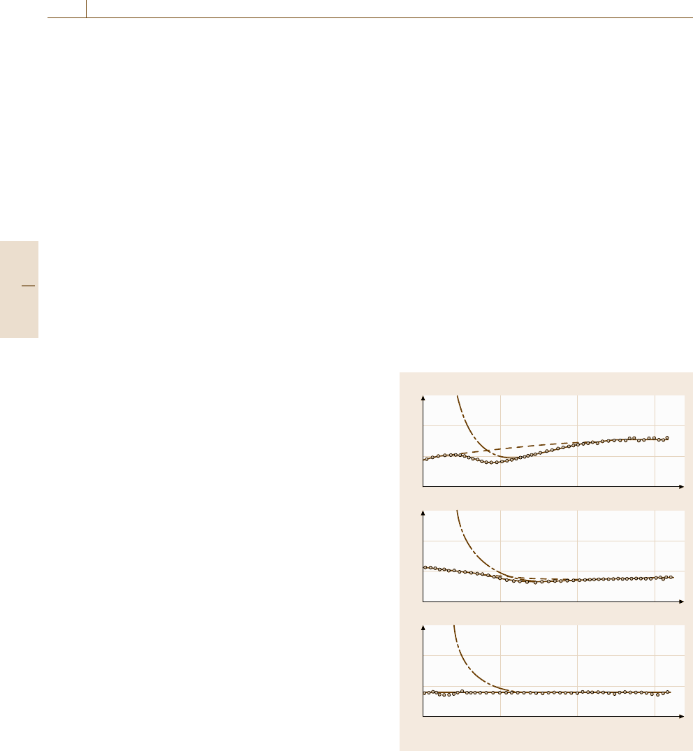
ing depth is lower than two Debye lengths. Figure 9.43
shows a typical comparison of uncorrected concentra-
tion profiles (dash-dotted lines) with the corrected ones
(circles). In both cases of boron and phosphorus doping
of the MIS capacitor, the correction algorithm delivers
relatively flat profiles. Without this correction pile-up
effects of the dopants were assumed due to annealing
and segregation effects. The precise determination of
the flatband point and the surface inversion point were
greatly improved by applying the Ziegler–Klausmann–
Kar profile correction [9.50]. The method is applicable
for quasi-static RF measured MIS C–V curves as well
as to pulsed RF C–V curves which avoid the surface
inversion of MIS structures during the short (ms) mea-
surement windows.
Measurement of Ion Implanted Profiles
In-depth profiling of ion implanted semiconductors is
a special challenge for the application of the depletion
approximation because a Gaussian-like implantation
profile has more or less steep edges around the max-
imum, i. e. around the average projected range of
deposited atoms. Furthermore, implantation profiles are
used, compared to diffusion doping profiles, to achieve
more abrupt doping transitions when scaling devices or
to achieve low-ohmic contacts. Thus, the steepness of
profile edges may occur easily within a Debye length,
especially for lower implantation doses.
The discussed correction algorithm of Ziegler
et al. [9.50] cannot be applied for smaller depth than two
Debye lengths. For larger depths this algorithm exhibits
Sample 1
Boron doped
Sample 2
Phosphorus doped
Sample 3
Phosphorus doped
2
1
0
2
1
0
2
1
0
N (10
16
cm
–3
)
N (10
16
cm
–3
)
N (10
16
cm
–3
)
Depth (μm)
0 0.1 0.2 0.3
Fig. 9.43 Examples for doping profiles in silicon MIS ca-
pacitors. The steeply uprising curves show the apparent
doping profiles using the uncorrected depletion approxima-
tion; the circles show the Debye-length corrected measure-
ments (after [9.50])
Part C 9.4
Electrical Properties 9.4 Semiconductors 517
Concentration
x
2ΔR
p
N
D
(x)
n(x)
1
e
Fig. 9.44 In-depth profiles of implanted dopants N
D
(x)
and free carrier concentration n(x): near the peak is
N
D
(x) > n(x)andfarawayfromthepeakisn(x) > N
D
(x)
a smooth transition into the standard depletion approx-
imation. Quite a lot of implanted profiles show their
projected ranges are quite deeper than several Debye
lengths.
The same problem arises during profiling of high–
low or low–high doping transitions of the same doping
type, e.g. in varactor diodes. In all these cases, lo-
cal charge neutrality is not fulfilled, especially in the
vicinity of the steepest doping gradient. This typical
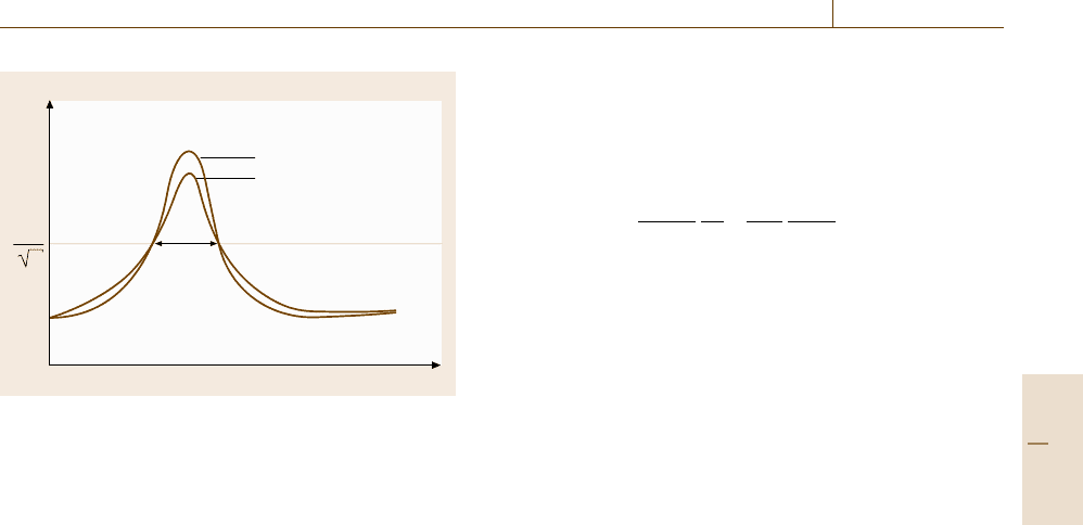
situation is explained in Fig. 9.44 using the example
of an implantation profile N
D
(x) with a Gaussian-like
shape of its edges. The mobile carrier concentration
n(x) deviates typically from the dopant distribution due
to spreading diffusion effects and repelling electrical
field forces, i. e. at the maximum, free carriers are miss-
ing and in the edges the mobile carriers produce longer
tails of the apparent concentration. This can be proved
by comparing SIMS (secondary ion mass spectroscopy)
measured implantation profiles with their C–V evalu-
ated counterparts. The C–V technique is based on the
signal from the mobile carriers (C = dQ/ dV ), thus
the apparent doping profile lacks the abruptness of the
real profile. Unfortunately SIMS cannot replace the
C–V evaluation because SIMS cannot measure the elec-
trically active concentration which is relevant for the
device function. It determines only the atom concen-
tration without information with respect to electrical
activation. Thus, an effort is needed to improve the C–V
evaluation in these applications. This improvement was
done by Kennedy et al. [9.51,52]. They developed a cor-
rection of the apparent depletion approximation profiles
assuming that the free carrier concentration is known.
Therefore, they solved Poisson’s equation considering
additionally the charge contributions of the majority
carriers and neglecting current flow in the reverse direc-
tion of Schottky- or pn-junction contacts. They deduced
(9.56) which extracts the dopant profile N
D
(x) from the
mobile carrier profile n(x)
N(x) =n(x)−
ε
0
ε
r
kT
q
2
d
dx
1
n(x)
dn(x)
dx
, (9.56)
where n(x) is obtained by evaluation of the standard
depletion approximation (9.54), (9.55) evaluation from
a C–V measurement. This extraction is valid if the true
mobile carrier profile would be known exactly. Un-
fortunately, the C–V measurement determines only an
approximation to this true mobile carrier profile because
the space charge edge is smeared out over about two De-
bye lengths. Thus, the Kennedy correction [9.51, 52]is
a useful improvement to obtain a more realistic shape
of implanted profiles but it cannot, in principle, provide
the true physical profile again caused by Debye length
reasons. A good rule of thumb in case of implanted
profiles, not to be affected too much by Debye length
distortions (error < 1%), is the relation ΔR
p
≥ 10L
D
,
with ΔR
p
being the half width of the implanted pro-
file and L
D
the Debye length for a given doping. This
means in practice that high-dose implanted profiles suf-
fer much less from Debye length distortions applying
the C–V technique.
Applying (9.56) for the improvement of step-like
high–low doping profiles, it is recommended (if pos-
sible) to provide the depletion from the highly doped
side because the Debye length is shorter at the begin of
the measurement which helps the accuracy of the profile
reconstruction [9.53].
Electron and Hole Effective Masses
The effective masses of mobile carriers in semi-
conductors reflect the curvatures of the band struc-
ture in the E(k) diagrammes. The effective mass
is of a tensorial type with components: 1/m
∗
ij
≡
1/
(
h/2π
)
2
[∂
2
E(k)]/(∂k
i
∂k
j
) with E denoting the band
energy and k (= 2π/λ) the wavevector of the carrier
related to its moment p = (h/2π)k. The band struc-
ture of semiconductors is described by Schrödinger’s
equation which is based on the wave nature of electron
propagation in crystals. Tabulated values of effec-
tive masses of common semiconductors can be found
in [9.49]. Effective masses can be measured by cy-
clotron resonance and by angle-resolved photoemission
spectroscopy (ARPES)[9.54]. III–V semiconductors
with their low effective electron masses (≈0.07) pro-
vide high carrier velocities within short acceleration
Part C 9.4