Czichos H., Saito T., Smith L.E. (Eds.) Handbook of Metrology and Testing
Подождите немного. Документ загружается.


518 Part C Materials Properties Measurement
times and thus a very high speed potential of electronic
circuits.
9.4.4 I–V Breakdown Mechanisms
Electrical breakdown in semiconductors is character-
ized in terms of the electrical field strength (unit
kV/cm) in regions of the I–V curve, where the cur-
rent increases to a much higher extent than for slightly
reduced field strength below. Electrical breakdown, in-
dicated by a steep current increase versus voltage, is
mainly related to two mechanisms: impact ionization
(avalanche) breakdown and tunneling (internal field
emission). Both mechanisms can be distinguished by
investigating the temperature behavior of the current-
voltage (I–V ) curves. For a certain constant voltage
in the breakdown region a positive temperature co-
efficient of the current is indicative for tunneling
breakdown, while a negative temperature coefficient
indicates impact ionization breakdown. Both mecha-
nisms are discussed in more detail in the following two
subsections.
Impact Ionization Breakdown Field Strength
Impact ionization is a bulk controlled current flow
mechanism induced by a carrier multiplying band–band
process. Carriers are accelerated by an high electrical
field, that they can induce electron–hole pair ionization
due to their high energy. The resulting additional elec-
trons and holes are accelerated in opposite directions,
until they gain and overcome their specific ionizing
energy (kT); thus, the whole process produces an
avalanche-like increase of the current after an only
small voltage increase. Impact ionization breakdown
can be concluded from a negative temperature coef-
ficient of the current at a high fixed reverse voltage.
Increasing temperature causes more lattice vibrations,
which hinder carriers, to gain directed acceleration; thus
higher electrical fields are needed at elevated temper-
atures, to produce the same current. Small effective
masses ease the ionization process due to higher car-
rier mobility in the accelerating field. Impact ionization
is a band–band pair generation process, thus the break
down electric field strength increases with increasing
bandgap of the semiconductor. The avalanche process is
described by the ionization rates α
n
and α
h
(unit 1/cm)
for electron or hole induced electron–hole pairs, respec-
tively. The ionization rates α
n,h
depend largely on the
electrical field strength E
α(E) =α
∞
e
[−(E
0
/E)
m
]
(9.57)
with α
∞
, E
0
,andm being a temperature dependent
material constant. Graphs of ionization rates of several
semiconductors can be found in [9.49] ranging up to
values of α
n,h
of 10
5
/cm.
Tunneling (Internal Field Emission)
Breakdown Field Strength
Tunneling or internal field emission is a quantum
mechanical process, where carriers penetrate through
thin energy barriers when the barrier thicknesses ap-
proach the value of the de Broglie wavelength (a few
nm). During the quantum mechanical tunneling pro-
cess their energy is conserved. Carrier tunneling is
a barrier-controlled current flow mechanism. Tunneling
is observed in highly doped pn junctions, where narrow
barriers are favored by the high doping and the resulting
small space charge regions. The de Broglie wavelength
λ
e,h
is given by
λ
e,h
=
h
2 ∗m
0
m
e,h
E
(9.58)
with m
0
denoting the free electron mass, m
e,h
the ef-
fective mass of electrons or holes, and E the energy of
the carrier. For, e.g. InP with an electron effective mass
of 0.07 and an electron energy of kT(T = 300 K)λ
e
amounts to 29 nm, while for E = 1eV, λ
e
reduces
to 4.64 nm.
The barrier to be penetrated by the carrier should be
narrower than de Broglie’s wavelength for the relevant
carrier’s energy. The probability for tunneling increases
considerably for electrical field strength in the range
of 10
6
V/cm, i. e. 1 (e)V/10 nm, where the effective bar-
rier width for band–band tunneling is reduced to 10 nm,
being in the range of the aforementioned de Broglie
wavelength. For this nonthermal process, the thermal
energy of the carrier (electron) is most often neglected.
Temperature Dependent Reverse Current
I–V Analysis
According to the explanations given in the two sub
sections before, the dominating mechanism for break-
down in pn-diodes or transistors can be identified by
measuring the reverse I–V characteristics for various
temperatures. A recommended temperature range ex-
tends, e.g. from 0 to 80
◦
C in steps of 20
◦
C, which can
be controlled by Peltier cooling or heating. Much wider
temperature ranges can be achieved in cryostats, where
electrical heating in conjunction with liquid nitrogen
cooling can provide a temperature range between 77
and 420 K. Because generation currents in pn-junctions
are increasing proportional to the intrinsic concentration
Part C 9.4
Electrical Properties 9.4 Semiconductors 519
n
i
, which itself increases exponentially over temper-
ature in half of a given bandgap; an even moderate
temperature spacing within a set of I–V curves results
in a current spread over about two orders of magnitude
in the low-field generation current regime. The current
versus voltage in this low-field generation regime in-
creases quite moderately with the square root of the
voltage. At the onset of either tunneling or avalanche
breakdown a much steeper increase of current is ob-
served. The following two figures of pn-diodes show
typical characteristics of either tunneling or avalanche
breakdown.
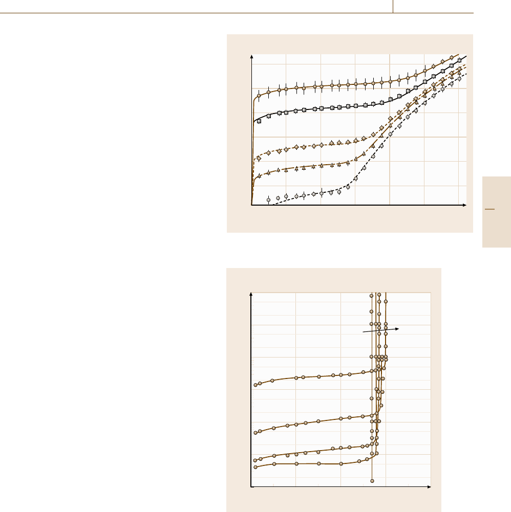
Figure 9.45 shows for a GaInAs homojunction pho-
todiode the typical band–band tunneling behavior for
voltages above of 15 V, where the remaining temper-
ature dependence stems from the decreasing bandgap
with increasing temperature. Thus, a positive tempera-
ture coefficient of the current for fixed voltage is present
in the tunneling region. Typical at the onset of tunneling
is a pronounced reduction of the temperature sensitivity
at the transition from the generation regime below 15 V
to the tunneling regime above 15 V.
Figure 9.46 presents the typical reverse current char-
acteristics of a silicon p
+
n diode [9.56] dominated
by avalanche breakdown above 27 V. Again, in the
lower field regime, the I–V characteristics show typi-
cal Shockley–Read–Hall generation behavior exhibiting
a pronounced temperature sensitivity according to the
higher bandgap of silicon (compared to Fig. 9.45)com-
prising a GaInAs photodiode. The onset of impact
ionization is characterized by a much steeper increase
of the current versus voltage compared to the tunneling
breakdown in Fig. 9.45. Furthermore, the temperature
coefficient is reversed compared to the tunneling case
before. In the impact ionization regime, a higher voltage
is needed for constant current with higher temperature,
due to increasing lattice vibrations which hinder the
electrons from being accelerated due to a higher colli-
sion rate. Thus, the I–V characteristics exhibit a typical
crossing behavior when the generation regime is taken
over by impact ionization.
In conclusion, the temperature resolved I–V char-
acteristics can clearly distinguish between generation,
tunneling and impact ionization regimes.
9.4.5 Deep Level Characterization
and Minority Carrier Lifetime
Deep levels in semiconductors heavily affect the for-
ward and reverse current curves they increase the noise
in photodiodes and transistors, reduce the minority
I
D
(A)
10
–5
10
–6
10
–7
10
–8
10
–9
10
–10
0 5 10 15 20 25 30
V
reverse
(V)
T =333K
285 K
230 K
208 K
156 K
N
D
=1.5× 10
16
cm
–3
A =2.9× 10
–4
cm
2
τ
eff
=15±2ns
Fig. 9.45 Dark current of a GaInAs homojunction photodiode (af-
ter [9.55]) dominated by tunneling breakdown above 15 V
Reverse current (A)
10
–4
10
–5
10
–6
10
–7
10
–8
10
–9
10
–10
Reverse voltage (V)
0 10 20 30 40
T
100 °C
45 °C
20 °C
2°C
–25 °C
Fig. 9.46 Reverse current of a silicon p
+
n diode (af-
ter [9.56]), dominated by avalanche breakdown above 27 V
carrier lifetime, or quench the storage time in charge-
coupled devices or CMOS focal plane arrays. One of
the most sensitive methods to determine a comprehen-
sive set of deep level or trap parameters is the DLTS
(deep level transient spectroscopy) technique.
Part C 9.4
520 Part C Materials Properties Measurement
Definition and Role of Trap Parameters
There is a common basis for the description of donor or
acceptor states and the so called deep levels or traps.
Donor or acceptor states are situated very closely to
the respective band edges in the band diagram (some
tens meV), while deep levels or traps have an energy
position more or less close to the midgap band en-
ergy, i. e. they are located deeper than 200 meV. The
equations for deep and shallow level ionization, which
are given in Sect. 9.4.2 are valid for dopants as well
as for deep levels or traps. The difference between
deep levels and traps is mainly attributed to their dif-
ferent interaction rates with both bands. While deep
levels often may interact with the conduction and va-
lence bands with comparable probabilities, traps are
exchanging their carriers dominantly on with one band.
This behavior is reflected by differences in energetic
positions: deep levels are close to the midgap energy
while traps are located near to one of the bands, but
considerably deeper than shallow donors or acceptors.
Thus, deep levels often function as recombination cen-
ters to extract electrons and holes from the bands under
nonequilibrium excitation conditions, while traps cap-
ture carriers from one of the bands within a very
short time constant (capture time constant in the ns
range) and emit these carriers back to the same band
after some delay (emission time constant in the ms
range). The temporal change of the total charge (ion-
ized dopants and deep levels) in the depletion region
of a Schottky diode affects the space charge capaci-
tance, which can be measured versus time to monitor
trap recharging processes. This field is called capaci-
tance spectroscopy [9.57], or more detailed deep level
transient spectroscopy (DLTS)[9.58].
Majority carrier traps Minority carrier traps
Electron trap
Hole trap
n-type semi-
conductor
p-type semi-
conductor
p-type semi-
conductor
n-type semi-
conductor
e
n
>> e
p
e
n
e
p
E
v
E
v
E
v
E
v
E
c
E
c
E
c
E
c
e
p
e
p
e
p
e
n
e
n
e
n
e
maj
>> e
min
e
min
>> e
maj
e
p
>> e
n
Fig. 9.47 Energetic location and main interactions of ma-
jority carrier traps and minority carrier traps in n- and
p-type semiconductors
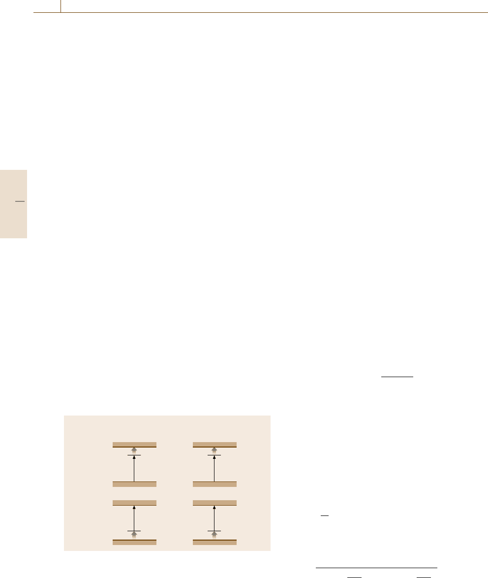
Figure 9.47 shows the principal possibilities for lo-
cating traps in the band diagrams of n- and p-type
semiconductors. The thick arrows indicate the domi-
nant interaction paths. If a trap is located much closer
to the conduction band than to the valence band (see
the electron traps in the upper parts of Fig. 9.47), then
their electron emission rates e
n
(unit s
−1
) are consider-
ably larger than their hole emission rates e
p
(unit s
−1
).
This situation reverses for hole traps located near to
the valence band. A trap interacting dominantly with
the majority (minority) carrier band is called a major-
ity (minority) carrier trap. A trap interacting dominantly
with the conduction (valence) band is called an electron
(hole) trap.
Traps are characterized by several parameters. The
first is the concentration N
T
(unit cm
−3
), the second is
the energetic distance from the corresponding energy
band edge E
c
−E
T
(E
T
−E
v
) (unit eV). The capture of
carriers represented by the capture rates c
n
, c
p
(unit s
−1
)
into traps from the bands is normally a very fast process,
the time constant of which is in the ns range
c
n
=σ
n
v
th
n and c
p
=σ
p
v
th
p , (9.59)
with σ
n
, σ
p
denoting the capture cross sections (unit
cm
2
, for orientation purposes 10
−15
cm
2
), v
th
denot-
ing the carrier thermal velocity (10
7
cm/s) and n, p the
carrier concentrations in the corresponding bands. Af-
ter the capture process the subsequent emission rate e
n
(unit s
−1
) is driven exponentially by the trap activation
energy E
c
−E
T
given here for an electron trap
e
n
=σ
n
v
th
N
c
g exp
−
E
c
−E
T
k
B
T
. (9.60)
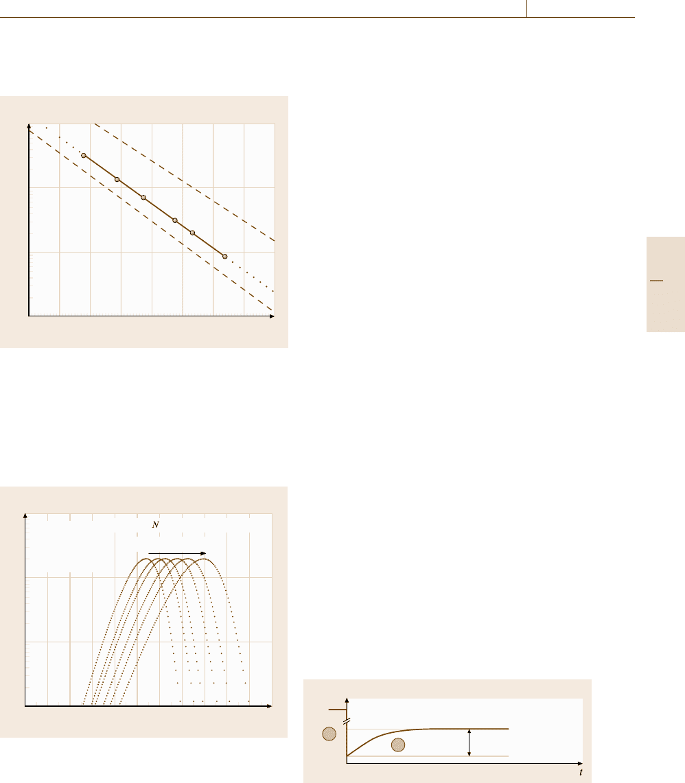
Equation (9.60) is the basis for the Arrhenius plot
which allows the extraction of the trap activation energy
by plotting log(e
n
/T
2
) versus 1000/T (Fig. 9.48). The
prefactor T
2
stems from the joined temperature behav-
ior of the effective densitiy of states N
c
in conjunction
with the thermal velocity v
th
.
The minority carrier lifetime τ
eff
(s) can be deduced
from the generation rate U (cm
−3
s
−1
) from the trap pa-
rameters according to the theory of Shockley, Read,and
Hall [9.59,60].
τ
eff
=
n
i
U
(9.61)
with n
i
denoting the intrinsic carrier concentration of
the semiconductor material [9.49]and
U =
σ
p
σ
n
v
th
N
T
σ
n
exp
E
trap
k
B
T
+σ
p
exp
−
E
trap
k
B
T
n
i
. (9.62)
Part C 9.4
Electrical Properties 9.4 Semiconductors 521
Here, E
trap
is the trap energy position with respect to
the intrinsic energy E
i
(E
i
≈(E
c
+E
v
)/2) of the semi-
Emission rate/T
2
(s
–1
K
–2
)
10
–1
5.2 5.4 5.6 5.8 6 6.2 6.4 6.6 6.8
10
–2
10
–3
10
–4
1000/T (K
–1
)
Fig. 9.48 Arrhenius plot of the DLTS spectrum in
Fig. 9.49 for Au in n-type silicon; the measurement is
shown as full line,thedashed lines represent comparison
data from a trap library to assess the measured Arrhenius
data compared to known data for easier identification. The
measured activation energy is 340 meV. The dotted line
is used for extrapolation of the capture cross section for
1000/T →0
ΔC
tot
(fF)
10
4
10
3
10
2
10
1
100 110 120 130 140 150 160 170 180 190 200 210
Temperature (K)
r/w
1000/s, 400/s
200/s, 80/s
50/s, 20/s
Rate windows (r/w)
Si at 13.3 V, N = 3.5 × 10
17
cm
–3
, C = 100 pF
Fig. 9.49 DLTS measurement of the Au trap in n-type sili-
con doped with 3.5×10
17
cm
−3
, reverse pulse: 13.3V.The
rate windows rw are from left to right:20/s, 50/s, 80/s,
200/s, 400/s, and 1000/s. The depletion capacitance is
100 pF
conductor. It can be seen from this equation that deep
levels near midgap are most effective for generation and
recombination because they lead to the largest genera-
tion or recombination rates U and thus give the lowest
minority carrier lifetime according to (9.61). Thus, it
is an important task of semiconductor materials qual-
ity assessment to determine the trap parameters N
T
, E
T
(respectively E
trap
), σ
n
,andσ
p
to deduce all further
generation and recombination statistics.
The DLTS Technique
The DLTS technique is based upon repetitive pulsing
the bias of a Schottky diode or pn-diode from slight for-
ward bias conditions (short pulse, some μs) into deep
depletion for a considerably longer time (ms to s) and
observe the resulting capacitance transient which stems
from the charging and emptying of traps. During these
repetitive measurements which also allow averaging of
the mostly relatively small capacitance transients, the
measurement temperature of the sample is varied over
a large range, e.g. from 77 to 400 K. The development of
this temperature dependent capacitance transient which
is directly indicative for trap charging and emission is
shown in more detail in this section.
Figure 9.50 shows the typical capacitance transient
for the emission phase 3 of a majority carrier trap, i. e.
a donor-like trap which is neutral in the electron occu-
pied or filled state and positively charged in the empty
state.
The process starts after phase (1), the empty (pos-
itively charged) state of all traps in reverse bias of
the sample (not shown in Fig. 9.50, this corresponds to
C(t) →∞), with a short filling pulse at t < 0, which
is in the range of some μs. The time period 2 is long
enough so that all majority carrier traps capture elec-
trons from the conduction band because in the forward
biased filling phase all traps are pulsed below the Fermi
energy E
F
. The traps are now neutrally filled at the
end of phase (2). The emission phase (3) is started by
pulsing the sample into deep depletion and the capaci-
tance drops to a minimum C(t = 0) =C
0
. The resulting
2
3
C(t)
C(t =0)
C(t →∞)=C
∞
ΔC
tot
= C
∞
– C
0
= C
0
Fig. 9.50 Transient capacitance during majority carrier
emission (3) after trap filling phase (2) of a donor-like trap
Part C 9.4
522 Part C Materials Properties Measurement
space charge depth is given by the bias voltage and
the depleted donor charge of the shallow doping level.
The traps are neutral at the beginning of the emission
phase (3) and thus they do not contribute to the de-
pleted space charge. Due to the high reverse bias V
r
in phase (3) all traps are pushed above the Fermi en-
ergy and they are switched to emission. The capacitance
transient C(t) in the emission phase can be calculated
with (9.63)
C(t) =
A
qε
0
ε
r
2
(
V
bi
+V
r
)
N
+
D
+N
T
1 −exp
(
−e
n
t
)
(9.63)
with A denoting the area of the Schottky diode and V
bi
representing the built-in voltage of the test diode. To-
wards the end of the emission phase (3) all traps are
empty, i. e. after loosing their electrons to the conduc-
tion band, the traps now contribute to the space charge
of the shallow donors N
(+)
D
with concentration N
(+)
T
.
The transient capacitance thus changes by an amount
ΔC
tot
=C
∞
−C
0
. From the amplitude ΔC
tot
of this
transient, the trap concentration N
T
can be deduced.
For large trap concentrations and thus large capaci-
tance transients, it may be practical to fit (9.63) with
a transient capacitance measurement to extract the trap
concentration. In practice, this direct way is difficult
when the trap concentration falls below the shallow
doping level by orders of magnitude. The transient will
be buried within the noise of the measurement. In 1974
Lang published a procedure to detect very small capac-
itance transients out of the noise even when the trap
concentration falls by 4–5 orders of magnitude below
the shallow doping level: the DLTS technique [9.58].
Two aspects are important. First, according to the
DLTS technique, the biasing sequence between filling
(slight forward direction) and emptying (reverse volt-
age V
r
) of the traps is applied repeatedly to the sample,
thus averaging of the transient can be reached. Sec-
ond, due to (9.60), the emission rate covers a very
large range of more than 10 orders of magnitude if all
possible trap positions between conduction band and
midgap are considered. This implies too much prob-
lems for standard electronics in covering this large
emission time range to measure the capacitance tran-
sient with sufficient resolution. Thus, the capacitance
transient is observed by sampling within a given time
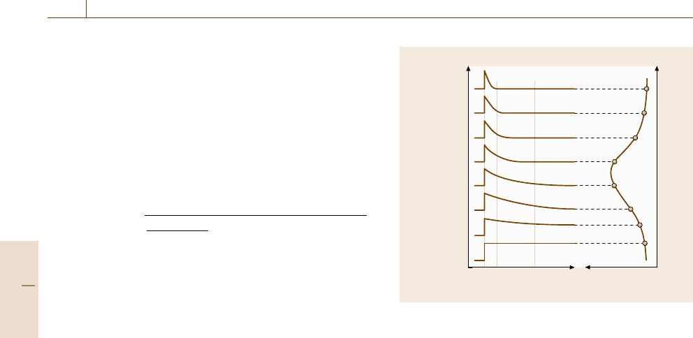
window called the rate window rw. The measurement
temperature is scanned such that the maximum of the
transient amplitude can be easily observed for any given
Capacitance transient C(t)
Temperature
Time DLTS signal
0–t
1
C(t
1
)–C(t
2
)t
2
Fig. 9.51 Construction of a DLTS signal (C(t
1
) −C(t
2
))
by observing the temperature depent transient capacitance
within an observation time window (t
2
−t
1
)
rate window rw. Figure 9.51 elucidates the principle
of Lang’s DLTS technique. For deep temperatures, the
emission process is very slow, thus the capacitance stays
practically constant over the observation time window
t
2
−t
1
. For high temperatures, the transient has oc-
curred completely even before the first sampling time
t
1
, thus the observed capacitance difference over t
2
−t
1
is again a constant. For a certain intermediate temper-
ature, where the trap emission rate fits the observation
time window, a maximum transient will be measured.
The DLTS signal (C(t
1
) −C(t
2
)) (right) is the differ-
ence capacitance over the rate window rw, according to
t
2
−t
1
. If a trap is very shallow, i. e. located energeti-
cally near to the band edge, quite deep temperatures are
needed to obtain the maximum of the DLTS signal.
The sign of the DLTS signal allows to determine
the trap type, ΔC
tot
> 0: majority trap and ΔC
tot
< 0:
minority carrier trap. Minority carrier traps in Schot-
tky diodes can be excited by applying pulsed optical
illumination (optical DLTS); in pn-diodes a sufficient
forward biasing is necessary to inject minority carrier,
to be trapped.
A typical DLTS measurement of the Au donor trap
in n-type silicon is shown in Fig. 9.49. The shift of the
DLTS peak to higher temperatures with increasing rate
window can be observed i. e. the emission rate increases
with increasing temperature. The trap concentration can
be determined from the amplitude of the DLTS signal.
For extracting the trap activation energy, the emission
rates need to be plotted in an Arrhenius plot over the in-
Part C 9.4
Electrical Properties 9.4 Semiconductors 523
verse of the temperature 1000/T. From the same plot,
the capture cross section for T →∞can be extracted
by extrapolating the emission rate for 1000/T → 0.
A corresponding Arrhenius plot of the measurement
in Fig. 9.49 is shown in Fig. 9.48. The measurement
of the emission rate, deduced from the DLTS signal
maxima for the different rate windows is shown in full
line, the dashed lines represent comparison data from
a trap library to assess the measured Arrhenius data
compared to known data for easier identification. The
measured activation energy is 340 meV. The dotted line
is used for extrapolation of the capture cross section for
1000/T →0.
The DLTS method cannot identify the physical na-
ture of a trap or a deep level, e.g. if the level originates
from a crystal defect or from an impurity. The big ad-
vantage of DLTS is its impressive sensitivity of N
T
/N
D
down to 10
−6
, unsurpassed by other physical analy-
ses. Trap concentrations as low as < 10
10
cm
−3
can
be detected, this is 13 orders of magnitude below the
crystals atomic concentration. Therefore electronic av-
eraging of the sampled small capacitance transients
applying boxcar or lock-in techniques are necessary.
DLTS delivers fingerprints of deep levels, which should
be compared to trap libraries of known defects, concern-
ing activation energy and capture cross section. DLTS
is spectroscopic, because traps with different activation
energies appear with their maxima at different tem-
peratures. If the spectra of two traps are overlapping,
subtraction methods can be applied by simulating and
approximating the DLTS maxima by Gaussian curves
with different slopes and subtracting the leading peak
from the rest of the spectrum until all traps have been
identified.
A lot of extensions of the DLTS technique have
been published. One important evaluation is the deter-
mination of the temperature dependence of the capture
cross section of a deep level [9.61], having in mind that
the standard DLTS technique allows only to measure
the extrapolated capture cross section for T →∞. The
method of Partin et al. is based on varying the width of
the filling pulse to very short times until the traps cannot
capture anymore carriers in the filling phase.
The Surface Recombination Velocity
Mesa diodes and also planar pn-diodes sometimes suf-
fer from additional leakage currents across the surface
or perimeter of the sample. Thus analyses of the bulk
currents are impeded by surface currents, which are in-
duced by additional surface recombination. The surface
recombination is described by the surface recombi-
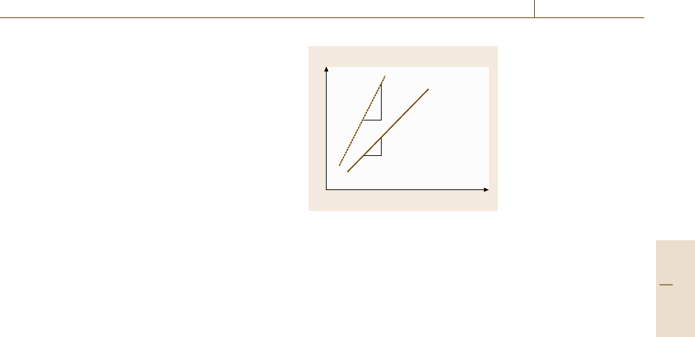
log I
log (diameter)
I ∼ πr
2
I ∼ 2πr
≈ 2
≈ 1
Fig. 9.52 Meas-
ured current of
a test diode in
double logarith-
mic plot versus
diode diameter
nation velocity S
0
(cm/s). Surface recombination or
generation occurs during nonequilibrium conditions,
e.g. under reverse bias of a pn-junction. A surface
recombination current j
s
(A/cm
2
) is directed perpen-
dicular to the semiconductor surface
j
s
=−qS
0
Δn , (9.64)
Δn is the deviation of the carriers from the equilib-
rium value. The surface recombination velocity S
0
can
be expressed by surface state parameters, like the cap-
ture cross section of the surface state σ
0
(cm
2
)andthe
concentration N
st
(cm
−2
).
S
0
=σ
0
v
th
N
st
. (9.65)
To identify whether a measured current of a test sam-
ple is dominated by bulk or by surface conduction,
a double logarithmic plot of the current versus the diam-
eter of the samples under test is helpful (Fig. 9.52). If
the current increases linearly with the diameter, then
surface recombination is dominant. If the current in-
creases quadratically with the diameter, bulk conduction
is dominant.
Bulk conduction should be proved before current
conduction mechanisms or parameters are extracted
from I–V measurements, like Schottky barriers, ide-
ality factors, Shockley–Read–Hall trap parameters, or
reverse current analyses are done with respect to tun-
neling or impact ionization.
9.4.6 Contact Resistances
of Metal-Semiconductor Contacts
Ohmic contacts at semiconductor devices are manda-
tory to connect the inner active regions to the outside
circuitry or other devices. Ideal ohmic contacts may be
described by several views of physicists or engineers
on the idealization of the tasks of ohmic contacts, i. e.
ohmic contacts should provide
Part C 9.4
524 Part C Materials Properties Measurement
Technical current
Metal
n-type semiconductor
E
f,m
E
max
E
a
V
f
E
c
E
f,s
δE
f,n
<0
1)
3)
2)
θ
θ
θ
θ
Φ
B
Fig. 9.53 Band diagram of a highly doped, degenerated
metal–semiconductor contact under forward bias condi-
tions (metal is positive with respect to the grounded n-type
semiconductor)
•
a bipolar linear I–V characteristics,
•
an unlimited high recombination rate for minority
carriers,
•
negligible voltage decay compared to that of the
active regions,
•
no minority carrier injection.
Basic work on the description and technology of ohmic
contacts to semiconductors can be found in [9.62, 63].
The main current conduction mechanisms in ohmic con-
tacts are elucidated in Fig. 9.53. A metal is evaporated
onto an n-type semiconductor. The work function differ-
ence to the electron affinity of the n-type semiconductor
should be well chosen to induce at best either an ac-
cumulation region at the semiconductor side or at least
a small barrier height Φ
B
. This has to be surmounted
or penetrated by electrons from the semiconductor, e.g.
here under forward biasing conditions. A more or less
small barrier is a usual case for a lot of metals to semi-
conductors. If the barrier cannot be avoided principally,
it should be only a small obstacle to be surmounted
or penetrated. Three current conduction mechanisms
should be mentioned here which help electrons to cross
the interface into the metal.
1. Thermal emission: electrons have to surmount the
barrier V
bi
(≈Φ
B
) which is only possible for a few
electrons with enough energy compared to the
thermal energy kT. Consequently, thermal emis-
sion results into bad ohmic contacts. Mostly, these
contacts exhibit rectifying characteristics at room
temperature. Thermal emission is favored exponen-
tially at high temperatures (thermal process).
2. Field emission or tunneling: this quantum mechan-
ical process allows electrons, due to their wave-like
nature, to penetrate the barrier without energy loss
if the barrier width is small compared to the de
Broglie wavelength (9.58). This process is likely at
very high degenerate doping levels ( 10
18
cm
−3
)
which induce very narrow space charge regions
(< 10 nm) and consequently very narrow tunneling
barrier widths. This process is nearly temperature
independent and useful even at very low temper-
atures because no thermal activation is needed for
quantum mechanical tunneling.
3. Thermal field emission or thermally activated tun-
neling: A certain part of the electrons are thermally
activated to penetrate the barrier at an enhanced en-
ergy position by tunneling but below the peak of the
barrier.
Both current conduction mechanisms 1. and 3. con-
tribute in series to the conduction over the barrier. Com-
pared to the aforementioned processes the electrons see
a smaller and narrower barrier. This mechanism is likely
for intermediate doping levels.
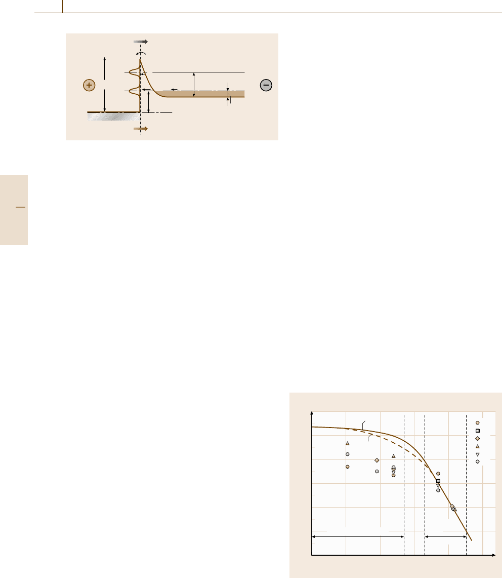
Figure 9.54 depicts the behavior of the contact re-
sistance of different metals on n-type silicon versus
the silicon doping level [9.63]. The contact resistance
(Ω cm
2
) strongly decreases with increasing doping level
when thermionic conduction is taken over by tunneling
or field emission.
Technically useful contact resistances should be
below 10
−5
Ω cm
2
. Thus, doping levels in excess of
10
19
cm
−3
are needed here to guarantee clear predomi-
nance of tunneling over thermionic emission. Values of
contact resistances lower than 10
−7
Ω cm
2
are achiev-
able today.
Contact resistance (Ω cm
2
)
10
4
10
15
10
16
10
17
10
18
10
19
10
20
10
2
10
0
10
–2
10
–4
10
–6
10
–8
N
D
(cm
–3
)
Thermionic emission
Thermionic
field
emission
B
A
Al
Cr
Co
Mo
Ni
V
Fig. 9.54 Contact resistance of various metals on n-type
silicon depending on doping N
D
(after [9.18])
Part C 9.4
Electrical Properties 9.4 Semiconductors 525
The more exactly termed specific contact resistance
R
c,spec.
(Ω cm
2
) is solely the contact resistance in the
interface between metal and semiconductor, while the
(total) contact resistance R
c
(Ω) comprises additional
contributions of the spreading resistance of the semi-
conductor which is depending on the current field lines
and thus on the geometry of the ohmic contact: distin-
guish contacts with vertical current spreading (e.g. top
contacts to lasers or emitter contacts to bipolar transis-
tors) and contacts with lateral current spreading (e.g.
base contacts in bipolar transistors or source/drain con-
tacts to field-effect transistors). The latter contact type
exhibits a strong inhomogeneous current density over
the contact length compared to the former contact type,
which has a better homogeneous current distribution
over its contact area.
Measurement techniques for contact resistances
may be attributed to the aforementioned contact geom-
etry. They should allow to extract the (low) specific
contact resistance from the (somewhat higher) total con-
tact resistance to provide information for optimizing the
contact resistance, e.g. by annealing procedures.
Measurements on ohmic contacts should be done
applying a Kelvin contact configuration which means
to feed a constant current via two terminals (needles) to
the pads of the contacts to be characterized and using
two different terminals (needles) to measure the result-
ing (small) voltage between the contact pads. In this
way, distorting effects of additional contact resistances
between the measurement needles and the contact pads
can be eliminated.
A method for characterizing contact resistances of
contacts with nearly homogeneous current flow into ver-
tical contacts uses contact dots of different diameters on
the semiconductor, to distinguish between the specific
contact resistance and the spreading resistance contri-
butions. This method by Cox and Strack is described
in [9.65].
A more versatile method which is mainly applied
to lateral contacts to thin semiconductor layers with
strongly inhomogeneous current flow, is the transmis-
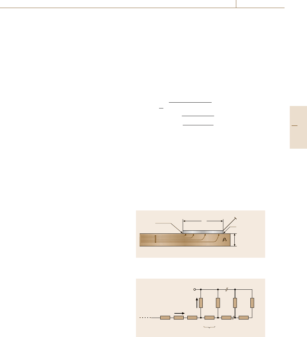
sion line method by Berger [9.64]. Figure 9.55 shows
the current distribution in this lateral contact type. The
semiconductor layer is assumed with a specific resis-
tance ρ
s
(Ω cm) and its sheet resistance R
s
(Ω/):
R
s
=ρ
s
/h. For technically relevant contacts, the semi-
conductor sheet height h is often quite less than the
contact length d. For this configuration, the following
equivalent circuit can be derived (Fig. 9.56). The resis-
tance of the epitaxial layer is described by the sum of its
differential elements dR
1
.
The specific contact resistance R
c,spec.
(=ρ
c
) is rep-
resented by the distributed vertical elements dR
2
. The
total contact resistance R
c
is the ratio of the voltage at
the left beginning of the contact region and the total
constant current I fed into the structure. According to
the transmission line nature of such a structure [9.64],
the specific contact resistance ρ
c
may be extracted from
the measurement of the total contact resistance R
c
.For
that purpose differential equations are formulated [9.64]
which can be solved giving a relation between total and
specific contact resistance in an implicit equation (9.66)
R
c
=
1
w
R
s
ρ
c
+0.2R
s
h
2
×coth
R
s
ρ
c
+0.2R
s
h
2
d
. (9.66)
This implicit equation allows the extraction of ρ
c
after
R
c
has been measured and the geometrical constants w,
h,andd of the test structure have been determined. The
sheet resistance R
s
of the epitaxial layer between two
contact stripes has also to be measured before.
The measurement of R
s
and R
c
can be done with
a setup of three contact stripes in a Kelvin contact con-
figuration with two distances l
1
and l
2
between two
contacts (Fig. 9.57).
High current
density
Low current
density
Contact metal
Epitaxial layer, thickness h
d
h
w
Fig. 9.55 Lateral contact of width w and of length d on
a thin epitaxial layer of thickness h (after [9.64])
x =0 x =d
V
i
dR
2
dR
2
dR
2
dR
2
dR
1
dR
1
dR
1
dR
1
dR
1
dR
1
I
i
dx
Fig. 9.56 Equivalent circuit diagram of a lateral ohmic
contact according to the current distribution in Fig. 9.55 for
the contact resistance of a metal on a thin semiconductor
layer
Part C 9.4
526 Part C Materials Properties Measurement
1
l
1
l
2
dw
23
Fig. 9.57 TLM mask for the determination of the sheet
resistance R
s
and total contact resistance R
c
from which
the specific contact resistance ρ
c
can be extracted (TLM:
transmission line model)
Two measurements need to be taken: first, the cur-
rent I (mA range) is fed through the epitaxial layer
stripe of width w by using the two left-hand contacts
1, 2 with distance l
1
and measuring the voltage V
1
; sec-
ond, the two contacts 2, 3 with distance l
2
are used to
measure the respective voltage V
2
by driving the same
amount of current through the epitaxial layer.
From these two voltage values V
1
and V
2
together
with the constant current I the sheet resistance R
s
and
the total contact resistance R
c
under each contact can be
calculated by
R
s
=
V
1
−V
2
l
1
−l
2
w
I
, and
R
c
=
1
2
V
1
I
−l
1
R
s
w
. (9.67)
With these two terms now (9.66) can be used to ex-
tract the specific contact resistance ρ
c
. The contact
distances l
1
and l
2
(1–100 μm) need to be determined
with high precision (submicrometer range) because oth-
erwise larger errors would result for ρ
c
, especially when
ρ
c
falls below 10
−6
Ω cm
2
.
For electrically long contacts (e.g. d = 40 μm) the
transfer length L
T
is defined as L
T
=
√
ρ
c
/R
s
. The
transfer length illustrates the typical length for the cur-
rent to pass from the epitaxial layer into the metal
contact. Practical contacts do not need to be designed
longer than about three transfer lengths.
The transfer resistance R
T
is defined as R
T
=
√
R
s
ρ
c
(Ω mm). The transfer resistance characterizes
the lowest contact resistance which can be achieved for
an electrically long contact of a given width w. Trans-
fer resistance values for e.g. FETs should be lower than
0.2 Ω mm.
9.5 Measurement of Dielectric Materials Properties
Dielectric materials are the building blocks of func-
tional electronic circuits, capacitors, gate dielectrics,
transmission lines are essential as electrical insula-
tors for power distribution. Molecular solids, organic
polymer resins, ceramic glasses and composites of
organic resins with ceramic fillers represent typical di-
electrics. The dielectric properties of materials are used
to describe electrical energy storage, dissipation and
energy transfer. Electrical storage is the result of dielec-
tric polarization. Dielectric polarization causes charge
displacement or rearrangement of molecular dipoles.
Electrical energy dissipation or loss results from
1. electrical charge transport or conduction,
2. dielectric relaxation,
3. resonant transitions and
4. nonlinear dielectric effects.
Energy loss is eventually related to scattering, radiation
or conversion of electrical energy into thermal energy
(Joule heating). Energy transfer is related to propa-
gation of electromagnetic waves in dielectric media,
transmission lines and waveguides, where the dielectric
permittivity determines the velocity of wave propaga-
tion, attenuation and ultimately the dimensions of the
devices.
It is important to understand the basic characteristics
of these processes because they determine the optimal
approach to measurement.
Interaction of electromagnetic radiation with mater-
ials at frequencies of about 10
12
Hz and above gives rise
to quantized transitions between the electronic, vibra-
tional and rotational molecular energy states, which can
be observed by using appropriate quantum spectroscopy
techniques. By contrast, the dielectric properties are
governed by reorientational motions of molecular
dipoles (dipolar relaxation) and motions of electrical
charge carriers (electrical conduction), which leads to
continuous dielectric dispersion and absorption that is
observed in the frequency range of 10
−6
–10
12
Hz.
The dielectric relaxation [9.66] describes the dis-
persion of real permittivity ε
and the occurrence
of dielectric absorption ε
. Permittivity measurements
Part C 9.5
Electrical Properties 9.5 Measurement of Dielectric Materials Properties 527
allows for the determination of molecular dipole mo-
ments and, subsequently, can link the relaxation process
with molecular dynamics and structure. The dielec-
tric absorption (loss) spectra as a function frequency
and temperature [9.67, 68], can be used to charac-
terize molecular dynamics in dipolar liquids (polar
solvents and solutes), rotator-phase crystals, nonpo-
lar and polar polymers (polyethylene, polyacrylates,
epoxy resins, polyimides). Research on dielectric relax-
ation in molecular liquids and solids was pioneered by
Fröhlich [9.69], Hill et al. [9.70], Bottcher and Bor-
dewijk [9.71], and for macromolecules by McCrum
et al. [9.72], and Runt and Fitzgerald [9.73]. Selected
developments in dielectric and related molecular pro-
cesss were reviewed by Davies [9.74]. Since 1954, the
most widely known and comprehensive work on di-
electric materials and corresponding measurements has
been that of von Hippel [9.75]. Measurement of RF
properties of materials were surveyed by Bussey [9.76].
Broadband waveguiding and free-space measurement
methodologies for the agriculture industry were devel-
oped by Nelson and coworkers [9.77, 78]. Extensive
dielectric data were obtained recently for ferroelec-
tric ceramics (barium titanate), inorganic and organic
semiconductors and photoconductors, for ultra thin di-
electrics films, which have important applications in
solid-state electronic circuits and devices. Recent ad-
vances in the theory of dielectric relaxation and the
corresponding experimental methodologies were re-
viewed by Kremer and Schönhals [9.79].
9.5.1 Dielectric Permittivity
The interaction of electromagnetic fields with matter is
described by Maxwell’s equations [9.80]. The polariza-
tion P describes the dielectric displacement D which
originates from the response of the material to an exter-
nal electric field E
P = D−ε
0
E =
ε
∗
r
ε
0
−ε
0
E , (9.68)
where ε
0
is the dielectric permittivity of free space
(ε
0
= 8.854 × 10
−12
F/m), and ε
∗
= ε
0
ε
∗
r
= ε
−iε
is
the complex permittivity tensor, which depends on
temperature, frequency, and in the case of anisotropic
materials, on the direction of the electric field vector E.
The frequency dependence of the permittivity is illus-
trated in Fig. 9.58.
Relative permittivity ε
∗
r
is a dimensionless ratio of
complex permittivity to the permittivity of free space
ε
∗
r
=ε
∗
/ε
0
=ε
r
−iε
r
. The dielectric constant is the real
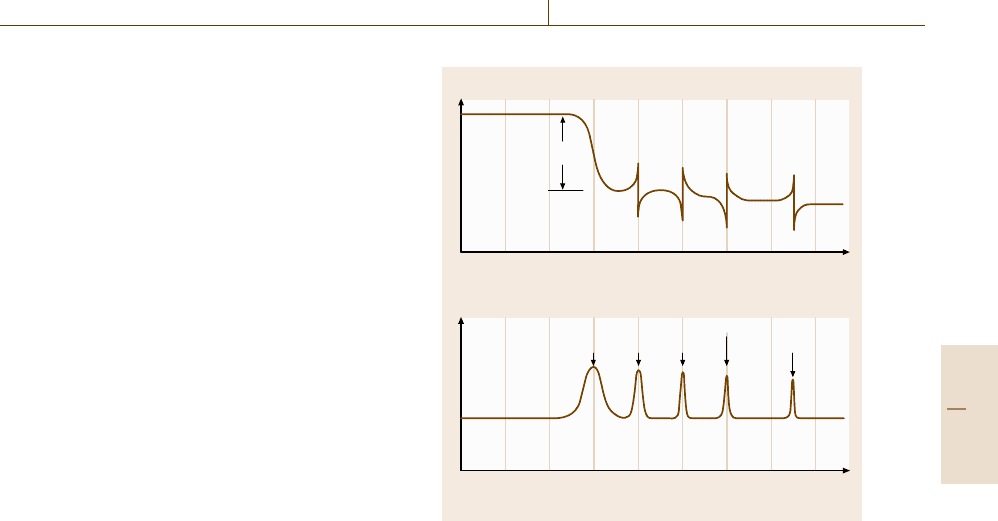
part of the relative permittivity. The symbol used in this
10
2
10
4
10
6
10
8
10
10
10
12
10
14
10
16
10
2
10
4
10
6
10
8
10
10
10
12
10
14
10
16
(Hz)
(Hz)
Atomic
Electronic
ε
r
'
ε
u
Δε
'
'
ε
r
''
f
r
f
LC
f
cav
Fig. 9.58 Frequency dependence of the real ε
r
,andimag-
inary ε
r
parts of the complex permittivity with a single
relaxation process at the relaxation frequency f
r
document is ε
r
(other symbols such as K, k, K
, k
, ε
r
and ε
are used in the technical literature). Dielectric
loss tangent tan(δ) is a dimensionless ratio of the dielec-
tric loss ε
r
to the dielectric constant ε
r
,tan(δ) = ε
r
/ε
r
.
Figure 9.58 illustrates that the real part of dielectric
permittivity decreases by Δε
r
at a certain frequency f
r
which gives rise to a corresponding peak of the dielec-
tric loss ε
r
. Such frequency dependence of the complex
permittivity indicates a dielectric relaxation. A dielec-
tric material may exhibit several dielectric relaxation
processes, each associated with its characteristic Δε
r
,
ε
r
and f
r
depending on the molecular mechanism in-
volved.
The dielectric relaxation should not be confused
with resonant transitions between vibrational and elec-
tronic states and those that originate from a resonant
behavior of the electrical measurement circuit.
Dielectric Relaxation
Unlike electrical conduction in which charge carriers
(electrons, ions and holes) move physically through the
material under the influence of an electric field, the
dielectric relaxation originates from reorientational re-
sponses of electric dipoles to the applied electric field.
Materials in which the dipoles are induced only by
the application of an electric field are nonpolar mater-
Part C 9.5