Henini M. Handbook of Self Assembled Semiconductor Nanostructures for Novel devices in Photonics and Electronics
Подождите немного. Документ загружается.

Self-organized Quantum Dot Multilayer Structures 9
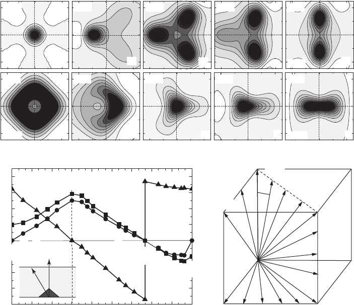
hard direction (i.e. (100) for ZnSe and (111) for PbTe) the strain energy minimum resides exactly
above the buried dot, whereas in all other cases the energy minima are laterally displaced by a
value r
min
. Even more, when the surface is close to an elastically soft direction, the central energy
minimum splits into several minima, as shown in panels (c) to (f) of Fig. 1.6 for PbTe and ZnSe.
(hkl)
1
0
1
101101101101101
PbTe
(a)
(100)
x/d parallel [011]
(b)
(211)
x/d parallel [111]
(c)
(111)
x/d parallel [-211]
(d)
(233)
x/d parallel [311]
PbTe
(e)
(011)
x/d parallel [100]
1
0
1
(f)
(100)
y/d parallel [0–11]
x/d parallel [011] x/d parallel [255]
(511)
(g)
x/d parallel [211]
(111)
x/d parallel [411]
(122)
ZnSeZnSe
x/d parallel [100]
(011)
45 30 15 15 30 45 60 75 90
40
30
20
10
0
10
20
30
40
PbTe
GaAs
ZnSe
PbTe
(k)
Inclination a of min. direction to [hkl] ()
(101)
(302)
(201)
(301)
(501)
(100)
(911)
(511)
(311)
(211)
(111)
(233)
(133)
(011)
(100)
(111)
(011)
(001)
(511)
(211)
(122)
(133)
(015)(013)
(l)
(101)
(201)
(311)
(233)
b
(j)
(i)
(h)
(hkl) Surface orientation β relative to [100] (°)
y/d dparallel [0–11]
0
01
1
01
1
01
1
01
1
01
1
Figure 1.6 Top : Calculated surface strain energy distributions Δ E
s
( x, y ) above a point-like strained buried
quantum dot for different surface orientations of PbTe (top row, A 0.28) and ZnSe (second row, A 2.52). The
energy distributions are shown as iso-strain contour plots as a function of reduced surface coordinates x/d and y/d ,
where d is the dot depth below the surface. Darker colours indicate areas of lower strain energy. For most surface
orientations the strain energy minimum is displaced from the centre above the buried dot. When the surface normal is
an elastically soft direction, a splitting into several side minima occurs. Bottom: (k) Inclination angle α at which the
energy minima appear on the surface relative to the ( hkl ) surface normal plotted as a function of the angle β between
the ( hkl ) surface and the (100) plane. The different ( hkl ) orientations are indicated in (l).
In the far-fi eld or point-source limit, the directions where the surface minima are formed are
unique for each surface orientation and elastic anisotropy ratio. This is because in this approxi-
mation the elastic strain fi elds do not depend on the structure of the dots but only on the elastic
properties of the matrix material. In addition, the surface strain distributions scale strictly lin-
early with the dot depth. This means that for each surface orientation there exists a well-defi ned
characteristic correlation angle α arctan( r
min
/ d ) along which the energy minima appear
on the surface relative to the surface normal direction. The directions within the surface along
which the surface energy minima are laterally displaced are also well defi ned and are given by the
CH001-I046325.indd 9CH001-I046325.indd 9 6/25/2008 12:27:14 PM6/25/2008 12:27:14 PM
10 Handbook of Self Assembled Semiconductor Nanostructures for Novel Devices in Photonics and Electronics
projection of the elastically hard direction closest to the surface normal onto the surface plane.
For example, for ( n 11) surface orientations, the lateral energy minima displacement within the
surface plane is along [
2nn
] for A 1 and along [
2nn
] for A 1 and n 1. Likewise, for (1 nn )
surfaces, the lateral displacement within the surface is along [
211n,,
] for A 1 and along
[
nn n,,1
22
] for A 1 and n 1. Finally, for (01 n ) surfaces, the displacement is along [
nn+1, ,
1
]
for A 1 and along [011] for A 1 .
Figure 1.6k shows the systematic variation of the correlation angle α as a function of the ( hkl )
surface orientation for three materials with different elastic anisotropy (GaAs, ZnSe, and PbTe).
In this plot, the ( hkl ) surface orientation is parameterized in terms of the angle β between [ hkl ]
and the [100] direction. Clearly, there is a systematic variation of α as the surface orientation is
tilted from (100) through (111) and (101) (see Fig. 1l). In particular, the largest interlayer cor-
relation angle appears when the surface is parallel to the elastically soft direction (i.e. (100) for
A 1 and (111) for A 1), whereas the energy minima are almost vertically aligned when the
surface is close to the elastically hard direction. Again it is evident that the behaviour is opposite
for materials with anisotropy ratio larger or smaller than one.
If we now compare materials with the same hard axis (i.e. ZnSe and GaAs in Fig. 1.6k ), one
can see that the larger the elastic anisotropy ( A
ZnSe
A
GaAs
), the larger the correlation angle and
thus the larger the lateral displacement of the energy minima. A systematic analysis of this trend
shows that the displacements and thus the correlation angles α depend in a linear way on the
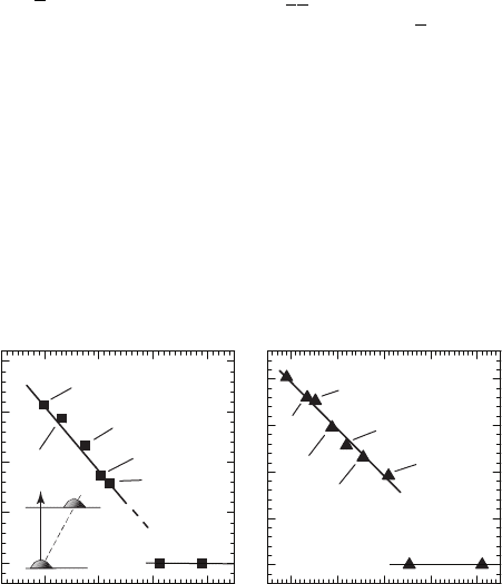
anisotropy ratio for A 1, respectively, on its reciprocal value for A 1 [56] . This is shown in
Fig. 1.7 , where the energy minima directions α are plotted for the most relevant high symmetry
(111) and (100) surface orientations as a function of elastic anisotropy. For the (100) direction
and the III–V and II–VI semiconductors ( Fig. 1.7a ), a splitting of the energy minima occurs if the
anisotropy exceeds the critical value of A
c
1.4, and beyond this value α varies linearly accord-
ing to [58] :
α
100
1
56 1 1 1 100 1 4
° (. ) () ..AAfor and
(1.4a)
Thus, α
100
increases from 16° to 23°, 28° and 32° for Si, GaAs, ZnSe and ZnS, respectively. For
the (111) surface direction and materials with rock salt structure ( Fig. 1.7b ), a splitting occurs
for A
c
0.6, and below this value, α varies according to [58] :
α
111
50 1 111 0 6 ° () () ..AAfor and
(1.4b)
Therefore, α
111
increases from 19° to 36° and 41° for PbS, PbTe and SnTe, respectively. A simi-
lar behaviour (increasing correlation angle with increasing elastic anisotropy) also applies for
other surface orientations. Apart from the changes in α direction, with increasing anisotropy the
0.4 0.6 0.8 1.0
0
10
20
30
40
(a) Inverse anisotropy ratio 1/A
ZnSe
BaF
2
C
Si
Ge
GaAs
ZnS
Minima direction α (°)
0.2 0.4 0.6 0.8 1.0
0
10
20
30
40
(b)
BaF
2
NaCl
AgBr
PbS
EuSe
EuTe
PbTe
PbSe
SnTe
Minima direction α (°)
Anisotropy ratio A
(001)
(111)
Figure 1.7 Direction α of the surface strain energy minima relative to a buried force nucleus plotted versus
elastic anisotropy of the matrix material for (a) the (001) surface and the group IV and the zinc-blende III–V
and II–VI semiconductors and (b) for materials with rock salt structure (IV–VI semiconductors, etc.) and (111)
surface orientation. In both cases, the surface normal direction is parallel to the elastically soft direction. The elastic
anisotropy is determined by the anisotropy ratio A 2 c
44
/( c
11
c
12
). Adapted from Holy et al. [56].
CH001-I046325.indd 10CH001-I046325.indd 10 6/25/2008 12:27:14 PM6/25/2008 12:27:14 PM
Self-organized Quantum Dot Multilayer Structures 11
depths of the energy minima also change. For the (100) surface the depth of the energy minima
increases with increasing anisotropy ratio, whereas for the (111) surface the depth decreases
with increasing A [58] . This is due to the fact that the anisotropy ratio represents the ratio of
Young’s modulus between the [111] and [100] directions.
1.3.2.2 Dot stackings in the far-fi eld limit
For multilayers with large spacer thickness compared to the dot size and little lateral overlap of
neighbouring dot strain fi elds, the far-fi eld strain calculations can be directly used to predict the
interlayer dot correlations in multilayer structures based on the assumption that the surface
dots are small enough to occupy just one strain minimum on the surface. From the calculations
shown in Fig. 1.6 , it then follows that for most materials and growth orientations inclined inter-
layer dot correlations should be formed, with dot correlation angles corresponding to those plot-
ted in Fig. 1.6k . This applies, e.g., to multilayer growth on high-indexed surfaces such as (211),
(311), (511) in which case the dots should replicate along oblique directions. This has indeed
been found by recent experiments by Schmidbauer et al. [142] for InAs/GaAs dot superlattice
growth on high-indexed ( n 11) substrate orientations. In fact, from the strain calculations for
elastically anisotropic materials an exact vertical dot alignment along the growth direction is
expected only when the surface orientation is parallel to the elastically hard axis, i.e. either for
the (111) or (100) surface of cubic materials. This is because in the far-fi eld limit only for these
surface orientations the strain minimum resides directly above the buried dots (see Fig. 1.6a and
h ). As shown in the next section, this also applies to multilayers with small spacer thicknesses.
A particular situation arises when the surface orientation is aligned or is close to the elasti-
cally soft crystal axis. If the elastic anisotropy is suffi ciently large, then the surface strain distri-
bution splits into several side minima above each buried dot (see Figs. 1.6 and 1.7 ). When one
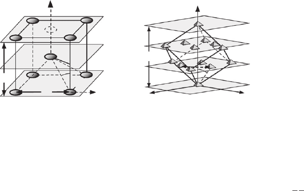
new dot nucleates at each of these minima, staggered dot stackings will be formed. For (001)
growth and an elastic anisotropy A larger than 1.5, four side energy minima occur above each
buried dot ( Fig. 1.6f ). These minima defi ne a preferred square arrangement of dots in the subse-
quent growth plane, with the previous dot located in the centre of the square below the surface.
This dot arrangement is replicated again in the subsequent dot layers, which in total results in an
ABAB... stacking sequence of dots, as shown schematically in Fig. 1.8a . In an ideal case, this will
yield an overall body-centred tetragonal 3D dot arrangement in the structures with a lateral align-
ment of the dots along the in-plane 100 surface directions .
For the (111) growth orientation and A smaller than 0.6, three side minima appear in the
energy distributions (see Fig. 1.6c ), which create a triangle with equal sides along the
〈〉211
sur-
face directions. This induces a triangular or hexagonal dot arrangement in the subsequent layer
centred above the buried dots underneath the surface. Each of these new dots will induce the
same triangular arrangement in the subsequent layer, and thus it takes in total three dot layers
(a) (b)
2d
3d
L
[100]
[111]
[001]
[010]
[112]
[110]
A
A
B
A
A
B
C
--
-
L
Figure 1.8 Staggered three-dimensional dot stackings expected from the point-source strain calculations for
materials with high elastic anisotropy and growth along the elastically soft direction. (a) ABAB … s tacking
and resulting body-centred tetragonal dot lattice for (001) growth and anisotropy ratio A 1.5, (b) fcc -like
ABCABC … dot stacking and resulting trigonal 3D dot lattice for the (111) growth orientation and materials with
A 0.6, as observed for PbSe/PbEuTe superlattices (see Fig. 1.2b ).
CH001-I046325.indd 11CH001-I046325.indd 11 6/25/2008 12:27:15 PM6/25/2008 12:27:15 PM
12 Handbook of Self Assembled Semiconductor Nanostructures for Novel Devices in Photonics and Electronics
until the dots appear again at the same position along the growth direction. This replication
thus produces an ABCABC … dot stacking sequence that is shown schematically in Fig. 1.8b . The
resulting dot arrangement is similar to the atom stacking in face-centred cubic lattices but in
general the ratio between the lateral dot spacing within the 2D sheet of hexagonally ordered dots
and the vertical spacer thickness will not be equal to 1.155 as in fcc lattices. Therefore, the dot
crystal lattice is expanded or compressed in the (111) direction, i.e. the 3D dot arrangement rep-
resents an overall trigonal lattice of dots. As shown in Fig. 3.4e, also for the (110) growth orienta-
tion two well-defi ned side energy minima may occur on the surface above the dots. Accordingly,
this may result in the formation of vertical sheets of 2D rhombohedrally ordered dots in a multi-
layer structure.
1.3.3 Near-fi eld strain interactions
For multilayers with small spacer layer thicknesses, the buried dots can no longer be approxi-
mated as simple point stress sources but their actual size, shape and gradients in compositions
must be taken into account. These parameters obviously differ strongly from one material to
another and moreover depend on the growth and overgrowth conditions, the dot layer thickness
and utilized growth technique (see, e.g., Stangl et al. [92] for a review). For (001) SiGe/Si dots,
e.g., hut cluster islands with { 105 } facets are formed at low growth temperatures and small cov-
erages [21, 124] , whereas for thicker dot layers and higher temperatures dome-shaped islands
with { 113 } facets are formed [125–127] , with several transitional shapes in between [126,
127] . Even steeper dots with { 111 } side facets have been observed for SiGe dots grown by liquid
phase epitaxy [104] . For (001) InAs/GaAs islands, on the other hand, multifaceted islands com-
posed of { 317 } , { 011 } and { 111 } facets have been reported [128, 129] , whereas for (111) PbSe
islands pyramids with triangular base and { 100 } side facets were observed [18, 130] . On high-
indexed surfaces, asymmetric island shapes have been found, such as for InAs on GaAs (113)A
[105] and Ge on (113) Si surfaces [106] . A further complication arises from the fact that during
overgrowth signifi cant changes in dot shape and composition occur due to intermixing with the
surrounding matrix material [92, 107–113] . This intermixing strongly depends on the growth
conditions [109, 110] as well as the chemical composition of the spacer layer [112, 113] and
changes the chemical composition of the dots as well [91, 110–113] . As a consequence, no gen-
eral solution of the near-fi eld strain interactions can be given but each particular experimental
situation and material system must be considered separately.
To calculate the strain fi elds of near-surface dots several methods have been used [92] . If the
elastic constants of dots and matrix material do not differ much, the strain fi elds can be obtained
by convoluting the point-source solution with the given dot shape [18, 92] . Alternatively, one
can also apply the fi nite element method [50, 110, 114, 118, 142] or atomistic calculations
using semi-empirical atom potentials [119–122] . These methods have been employed exten-
sively for InAs/GaAs [93, 117, 119] and Si/Ge [110, 118–121] dots but also for other materials
such as InN/AlN [84, 123] . As shown by Pryor et al. [119] , all three methods give quite similar
results for the strain fi elds well outside of the buried dots, as applies for the surface strain fi elds
well above the dots relevant for multilayer structures. As a general trend, for near-surface dots
the strain fi elds are focused towards the surface normal direction, i.e. the surface energy minima
are confi ned more closely to the region directly above the buried dots. This arises from the fact
that the free surface allows a very effi cient strain relaxation due to the outward or inward relaxa-
tion of the surface lattice planes.
1.3.3.1 (100) surfaces
For (100) surfaces, the changes of the strain energy distributions in dependence of the dot
depth are demonstrated in Fig. 1.9 for InAs dots embedded in GaAs. In this example, the dots
were assumed as truncated square base InAs pyramids with a fi xed base width of 20 nm and a
height of 7 nm (see insert of Fig. 1.9 ), similar to what has been found in cross-sectional scan-
ning tunnelling microscopy studies [72, 73, 111] . For simplicity, variations in the chemical com-
position within the dots due to intermixing [92, 111] were neglected, i.e. pure InAs dots were
CH001-I046325.indd 12CH001-I046325.indd 12 6/25/2008 12:27:15 PM6/25/2008 12:27:15 PM
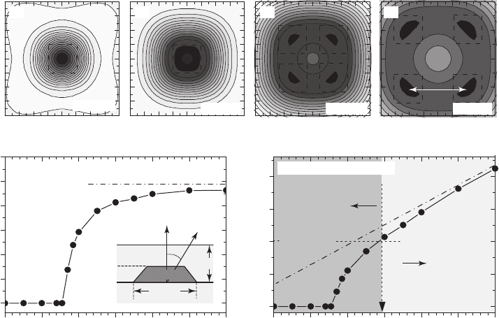
Self-organized Quantum Dot Multilayer Structures 13
assumed. The strain energy distributions were calculated using the semi-analytical method [92]
and the GaAs spacer thickness was varied from 10 to 70 nm. Figure 1.9a–d shows representative
energy distributions for dot depths of d 20, 30, 50 and 70 nm, respectively. Whereas for large
dot depths of d 5 0 n m ( i . e . d larger than two times the dot width), the surface strain distribu-
tions exhibit four side minima along 110 in good agreement with the point-source model (com-
pare Fig. 1.9c and d with Fig. 1.6f ), with decreasing dot depth the lateral spacing of the energy
minima rapidly shrinks and eventually they merge into one single minimum located directly
above the dot ( cf. Fig. 1.9a ). This clearly demonstrates the focusing of the strain fi elds in the verti-
cal growth direction when the dots reside very near to the growth surface.
Figure 1.9e shows the directional angle α of the surface energy minima relative to the surface
normal as a function of the GaAs spacer thickness. For large spacer thicknesses, α converges to
the value of 24° obtained from the far-fi eld (point-source) approximation. At spacer thicknesses
lower than 40 nm, however, α rapidly drops to zero such that at d 25 nm only one central
minimum is formed. Thus, a spacer thickness of more than four times the dot height is required
in order to get any splitting of the strain energy minima on the surface. Similar results were
also obtained by other works for slightly different geometries for the buried dots [93, 94, 96] .
The dependence of the lateral energy minima separation L on dot depth is shown in Fig. 1.9f .
For large d , α is constant and L increases essentially linearly with increasing spacer thickness
as expected from the point source approximation (dashed line in Fig. 1.9f ). Below d 4 0 n m ,
L rapidly decreases and drops to zero when d reaches 26 nm. As a consequence, for superlattices
with small spacer thicknesses the InAs dots will always be vertically aligned. To obtain a stag-
gered ABAB … dot stacking, the spacing of the energy minima L must be larger than the base
10 20 30 40 50 60 70
0
5
10
15
20
25
30
10 20 30 40 50 60 70
0
10
20
30
40
403020 010 2010 30 40 3020 010 2010 30 40 3020 010 2010 30 40 3020 010 2010 30 40
40
30
20
10
0
10
20
30
40
(a) (b) (c)
x along [100] (nm)
y along [010] (nm)
x along [100] (nm) x along [100] (nm) x along [100] (nm)
L
Point source
(e) Correlation angle
Correlation angle (deg)
Point source
Staggered
ABAB stacking
(f) Minima separation L
Spacing of energy minima (nm)
InAs dot depth d(nm)
b 20 nm
d
c
40 nm
GaAs
20 nm
7nm
d 30 nm
d 50 nm
d = 70 nm
d 20 nm
InAs dot depth d (nm)
Vertically
aligned
L b
L b
InAs
d
(d)
Figure 1.9 Top : Iso-strain energy contour plots of the surface strain energy distribution above a buried InAs
quantum dot with truncated pyramidal shape, 20 nm base and 7 nm height located in a GaAs matrix at different
dot depths of d 20, 30, 50 and 70 nm from (a) to (d), respectively. The darker colour corresponds to lower strain
energy on the wetting layer, and the separation of the contour lines decreases each by a factor of four from 0.2 meV
to 0.003 meV per atom pair from (a) to (d), respectively. The dashed squares indicated the base of the InAs islands.
Bottom : (e) Direction α of the energy minima relative to the surface normal as well as (f) lateral separation L of the
energy minima plotted as a function of the InAs dot depth. The dash-dotted lines indicate the results of the point-
source model for comparison.
CH001-I046325.indd 13CH001-I046325.indd 13 6/25/2008 12:27:16 PM6/25/2008 12:27:16 PM
14 Handbook of Self Assembled Semiconductor Nanostructures for Novel Devices in Photonics and Electronics
width b of the dots which is indicated by the horizontal dashed line in Fig. 1.9f . Accordingly, the
GaAs spacer thickness must be larger than a critical thickness of d
c
40 nm (see Fig. 1.9f ). This
is in agreement with recent experiments by Wang et al. [87] , where a transition between verti-
cally aligned and staggered InGaAs/GaAs dots was observed at spacer thicknesses around 40 to
50 nm. On the other hand, the depth of the energy minima becomes very shallow at large dot
depths. Therefore, there is only a limited range of parameters where a staggered dot stacking can
be achieved. This will be discussed in more detail in Section. 1.3.4.
The transition in InAs dot stacking clearly depends on the given dot size, i.e. for larger dots with
wider base b , the transition to a staggered dot stacking will occur at a larger critical spacer thick-
nesses d
c
. If the aspect ratio, i.e. shape of the dots, is constant, the length scale of the strain distri-
butions scales linearly with the system size, whereas the directional angles α of the surface strain
minima are constant for a given b / d ratio. The minima separation L can then be easily recalcu-
lated from Fig. 1.9 by applying a linear scaling factor of b / b
0
where b
0
is the 20 nm base width
used in the present calculations. Thus, for two times larger dots ( b / b
0
2), the minima angle α
of Fig. 1.9 appear at two times larger spacer thicknesses at which the minima separation L is
twice as large. Therefore, in this case the expected transition from vertically aligned to staggered
dots is shifted to a two times larger spacer thickness of d
c
80 nm.
The conclusions from the InAs/GaAs strain calculations apply for all zinc-blende III–V and
II–VI semiconductors because the elastic anisotropy is quite similar or even larger than for the
InAs/GaAs system ( cf. Fig. 1.5 ). For CdSe dots in ZnSe, e.g., surface strain distributions have been
calculated by Quek and Liu [94] for pyramidal dots with 20 nm base and 10 nm height using the
fi nite element method. As a result, a vertically aligned surface strain minimum was found up to
20 nm ZnSe spacers, but a lateral minima splitting of 16 nm was found already for 30 nm spacers
[94] . This means that due to the higher elastic anisotropy of ZnSe compared to GaAs ( A 2 . 3
versus 1.83, respectively), the splitting occurs already at a spacer thickness of three times the
island height. At 40 nm ZnSe thickness, the minima spitting is already as large as 33 nm, indicat-
ing that under these conditions the strain fi eld is already close to the point-source approximation
(splitting of 42 nm).
We have also performed strain calculations for the Ge/Si (100) case assuming pyramidal dots
with 50 nm base and 10 nm height. As a result, we fi nd that even up to 100 nm Si spacers only
one vertically aligned surface strain energy minimum is formed above each dot. This is due to the
smaller elastic anisotropy. Even in the far-fi eld limit the splitting of the surface energy minima is
about 40% smaller than for the InAs/GaAs case. Since Ge dots also exhibit a much wider island
shape, spacer thicknesses much larger than 100 nm would be required to obtain a suffi ciently
large energy minima splitting to induce a staggered ABAB … dot stacking in the SiGe/Si system.
This is well beyond the spacer layer thicknesses up to which interlayer correlations have been
observed in this material system [19, 32, 34–36] (see Section 1.7). As a consequence, there
seems to be little chance for obtaining a staggered dot stacking in the Si/Ge system.
1.3.3.2 (111) surfaces
For materials with elastically hard axis along [111] (i.e. with A 1 such as for SiGe, III–V and
II–VI materials), the point-source model already yields only a single energy minimum directly above
each dot. Therefore, for extended dots and thin spacer layers no change in this respect occurs in
the near-fi eld limit but only the overall shape of the energy distributions around the central mini-
mum is somewhat changed in dependence on the lateral extend and shape of the buried dots. The
situation is different for IV–VI materials where [111] is the elastically soft direction and thus a
three-fold minima splitting is found in the far-fi eld limit. We have evaluated in detail the changes
of the (111) near-fi eld strain distributions as a function of dot size [55] and spacer thickness [50]
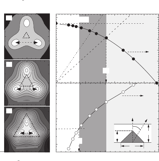
using the fi nite element method. Figure 1.10a to c shows the calculated strain energy distribu-
tions for pyramidal PbSe dots within a PbTe matrix at a fi xed dot depth of 42 nm but variable dot
height h (see inset of Fig. 1.10e ). The shape of the dots was kept constant with a fi xed aspect ratio
of h / b 2.45. Although the spacer thickness is constant in this case, clearly the separation of
the three surface strain minima L
min
indicated by the arrows in Fig. 1.10a–c shrinks as the size of
the buried dots relative to the spacer thickness increases, i.e. as the top of the buried dot pyramids
CH001-I046325.indd 14CH001-I046325.indd 14 6/25/2008 12:27:16 PM6/25/2008 12:27:16 PM
Self-organized Quantum Dot Multilayer Structures 15
moves closer to the epilayer surface. This is shown in Fig. 1.10d , where the separation L
min
of the
energy minima is plotted as a function of PbSe dot height.
For small dots, the minima separation is equal to that of the point-source model (horizon-
tal dashed line). As the dot height increases above 10 nm, the minima separation gradually
decreases and reaches zero for a dot height larger than about 30 nm. This is again caused by
the focusing of the strain fi elds in the surface normal direction. Similar results were obtained
for PbSe dots with fi xed 12 nm height but varying dot depths [50] (see Section 1.8 for details),
in which case a splitting of the surface strain minima occurs only when the spacer thickness is
larger than about 16 nm, whereas for thinner spacers again only one vertically aligned central
strain minimum is formed. Thus, for this material system, due to the substantially higher elastic
anisotropy compared to III-V materials, a splitting of the strain minima occurs when the spacer
thickness is two times larger than the dot height. In addition, the overall strain distributions are
found to agree well with those of the point-source model at a d / h ratio above 3, where the corre-
lation direction of the strain minima from the fi nite element calculations of α 31° are already
close to the far-fi eld value of 36 °. This means that the point-source approximation can be readily
applied for spacer thickness three times larger than the dot height.
0 5 10 15 20 25 30 35
0
10
20
30
40
50
60
0.0 0.2 0.4 0.6 0.8
0.1
1
10
Minima spacing L
min
(nm)
Point source
Depth of energy
minima E
min
(e)
40
0
40
40 0
40
40 0 40
40
0
40
y || [112] (nm) y || [112] (nm) y || [112] (nm)
40
0
40
PbTe
b
PbSe
(111)
h
x || [110] (nm)
x || [110] (nm)
PbSe dot height h (nm)
Scaled PbSe dot hei
g
ht h/d
b
h√6
b L
min
b L
min
fcc
stacking
Uncorrelated
E
crit
h
c
1
h
c
2
h ⴝ 6 nm
L
min
h ⴝ 12 nm
L
min
h ⴝ 24 nm
L
min
Separation of
minima L
min
(d)
E
min
w
eff
1.5 b
Vertical
alignment
d 42 nm
E
min
(meV/atom pair)
(a)
(b)
(c)
Figure 1.10 Left-hand side (a) to (c): Iso-strain energy contour plots of the surface strain energy distribution
above pyramidal PbSe quantum dots with different heights of 6, 12 and 24 nm, respectively, buried below a 42 nm
PbTe (111) spacer layer. The dot base is indicated by the dashed triangles. The contour line separation is 0.046,
0.13 and 0.65 meV/atom pair from (a) to (c), respectively, and the brighter colour corresponds to lower strain
energies. Right-hand side : Plot of the dependence of the separation L
min
(d) and depth E
min
(e) of the energy minima
as a function of PbSe dot height. In (d), the change of the dot base width b h
6 as a function of dot height is
plotted as a dashed line as well as the effective width (dash-dotted line) of the denuded zone w
eff
1 . 5 b around
each dot where further dot nucleation is suppressed. In the left region, the depth of the energy minima becomes
insuffi cient to cause a correlated dot nucleation. From experiments this is deduced about 0.3 meV/atom pair [50] .
The central region corresponds to the conditions where an fcc -like dot stacking is predicted. In the right region the
minima separation is smaller than the dot base width and therefore the dots are expected to be vertically aligned.
These predictions are in quite good agreement with experimental observations [55] .
CH001-I046325.indd 15CH001-I046325.indd 15 6/25/2008 12:27:17 PM6/25/2008 12:27:17 PM
16 Handbook of Self Assembled Semiconductor Nanostructures for Novel Devices in Photonics and Electronics
Concerning the dot stacking in multilayers, for formation of an fcc -like dot stacking as shown
in Fig. 1.8b , the minima separation must be larger than the dot base width b h
6 indicated by
the dashed triangles in Fig. 1.10a–c . From the crossing of the diagonal dashed b h
6 line in
Fig. 1.10d with the L
min
( h ) curve, one can infer that this condition is met only when the ratio
between the dot height and spacer thickness is smaller than about 0.4, i.e. for dots smaller than
15 nm for d 42 nm, which agrees well with our experimental observations [55] . Figure 1.10e
also shows the dependence of the energy minima depth on dot size. Clearly, the depth decreases
very rapidly with decreasing dot height, since the elastic strength of the buried dots is propor-
tional to their volume that scales as h
3
( cf. Eq. 1.2 ). From experimental studies on PbSe dot super-
lattices, no interlayer correlations were observed when the depth of the energy minima is smaller
than about 0.3 meV/atom pair [50] . According to Fig. 1.10e , this point is reached when the dot
height drops below 7 nm, in good agreement with experimental observations [55] . Thus, fcc
stacked PbSe/PbTe dot multilayers can only be obtained for certain dot sizes and spacer thick-
nesses. This general conclusion holds for all material systems and is discussed in Section 1.3.4.
1.3.3.3 High-indexed surfaces
For high-indexed surfaces, only recently fi nite element calculations of the strain fi elds of bur-
ied dots have been performed by Schmidbauer et al. [142] in order to model the interlayer cor-
relations of InGaAs/GaAs dot superlattices. For a constant 33 nm GaAs spacer thickness, it was
found that for the ( n 11)B surfaces the inclined energy minima directions above lens-shaped
InGaAs dots with 5 nm height and 30 nm width agree well with those predicted by the point-
source model (see Fig. 1.6k ). The results of these calculations are presented in more detail in
Section 1.4.3 and are displayed in Fig. 1.17c . Although, the fi nite element calculations were not
extended to thinner spacer layers, from the results of the previous sections it is evident that for
near-surface dots the surface minima will be confi ned closer to the surface normal direction. In
this case, the interlayer dot replication angles will become smaller than predicted by the far-fi eld
approximation of Fig. 1.6k . The fact that the experimentally measured interlayer correlation
directions in InGaAs/Gas dot superlattices on high-indexed surfaces [142] were found to agree
well with the angles predicted by the point-source model again shows that this approximation
works well already for spacer thicknesses of 33 nm as used in these experiments.
1.3.4 Stacking conditions and replication angles
According to the near-fi eld strain calculations, in multilayers with small spacer thicknesses the
dots should be always vertically aligned, whereas staggered or inclined dot correlations can occur
only for spacers exceeding a certain critical thickness value d
c
1
. With increasing spacer thickness,
on the other hand, the strain fi elds of buried dots rapidly decay such that above a certain critical
thickness d
c
2
no interlayer correlations will be formed any more. Up to now, we have also not con-
sidered the infl uence of overlapping strain fi elds of neighbouring buried dots that may modify
the surface strain distributions and thus the interlayer correlations as well. These three aspects
are analysed in more detail in the following to derive some generic rules for the stacking and cor-
relations in multilayer structures. These conditions will be compared with experimental results
in Sections 1.5–1.8.
1.3.4.1 Correlated–uncorrelated transition
As revealed by various growth studies, interlayer dot correlations in multilayer structures typi-
cally persist to spacer thicknesses up to around 40 to 70 nm for different material systems [15,
35, 36, 45, 50] as will be shown in detail in Sections 1.6–1.8 for the InAs/GaAs, Si/Ge and
PbSe/PbEuTe systems. Although the limiting thickness for interlayer correlations d
c
2
actually will
depend on parameters such as growth conditions [45, 56] and size of dots [55] , it is remark-
able that the experimental values are quite similar for the different material systems. The critical
thickness for interlayer correlations is mainly determined by the magnitude of the surface strain
energy minima induced by the buried dots. These can be easily calculated since for large spacer
thicknesses the point-source approximation holds. For a given ( hkl ) surface orientation, the depth
CH001-I046325.indd 16CH001-I046325.indd 16 6/25/2008 12:27:17 PM6/25/2008 12:27:17 PM
Self-organized Quantum Dot Multilayer Structures 17
of the energy minima Δ E
s,min
produced by buried dots then depends only on the dot volume V
0
and dot depth d , as well as the lattice mismatch ε
0
and the elastic constants and orientation of
the materials. Similar to the isotropic case (Eq. 1.2 ), in the far-fi eld limit the depth of the energy
minima Δ E
s,min
can be calculated by the simple expression of
ECEVd
shkls
D
,
/.
min
2
0
3
(1.5)
In this expression, E
s
2D
K
hkl
ε
0
2
is the strain energy density of the biaxially strained 2D wetting
layer, where K
hkl
2 μ (1 ν )/(1 ν ) is given by the elastic constants and growth orientation.
For the three material systems, e.g. Si/Ge, InAs/GaAs, PbSe/PbTe, the 2D misfi t strain energy E
s
2D
turns out to be of the same order of magnitude of ~100 meV/atom pair. C
hkl
is a dimensionless
constant that takes into account the elastic anisotropy and the dependence of the surface strain
distributions on the ( hkl ) surface orientation. From the far-fi eld strain calculations of Section
1.3.2, C
100
0.5 for (100) Si and GaAs and 0.56 for ZnSe, and it is C
111
0.69 for (111) PbTe
or PbSe (see also [58] ). For the isotropic case, C
iso
2 ( 1 ν )/ π 0.83 according to Eq. 1.2 .
To assess the remaining parameter of the island volume, it is noted that self-assembled quantum
dots usually exhibit a well-defi ned shape that is defi ned by low-energy side facets. For Ge hut clus-
ter islands (which we consider here), these are { 105 } facets [19, 124] , or higher-indexed facets for
the larger dome-shaped islands [19, 125–127] . For InAs islands, several different facets have been
reported [128, 129] , but for simplicity we approximate them by pyramids with { 113 } facets. (111)
PbSe islands exhibit a triangular pyramidal shape with { 100 } facets [130] . Using typical dot base
widths of 60 nm for Ge and 30 nm for InAs and PbSe islands, one can estimate the corresponding
island volumes to be 7200, 4270 and 1600 nm
3
, respectively, which is assumed to be preserved
during overgrowth. Using these values for Eq. 1.5 , it turns out that the experimental cut-off spacer
thickness d
c
2
of about 50 nm for the depths of the surface strain energy minima Δ E
s,min
is only
1–2 meV per atom pair for all three material systems. This shows that surprisingly low surface
strain energy variations are suffi cient in order to induce a correlated dot nucleation in multilayer
structures. In fact, taking into account the signifi cant intermixing of Stranski–Krastanow dots
with the surrounding matrix material [92, 107–113] the magnitude of the energy minima will
be further reduced. Although the interaction energies represent only rough estimates, it is evident
that the obtained critical magnitude of surface strain energy variations is not only a factor of more
than 20 smaller than the homogeneous misfi t strain energies E
s
2D
of the 2D wetting layer, but also
more than one order of magnitude lower than the typical thermal energies k
B
T during growth. It is
therefore an open question to explain how such small energy variations can infl uence diffusion of
surface adatoms enough in order to trigger correlated dot nucleation in multilayer structures. As a
result, the exact microscopic mechanism of correlated dot nucleation still remains to be clarifi ed.
1.3.4.2 Vertically aligned–staggered stacking transitions
According to the near-fi eld strain calculations, for near-surface dots the strain fi elds are strongly
focused along the surface normal direction. Therefore, in multilayers with small spacer thick-
nesses the dots should be always vertically aligned. In the far-fi eld limit, on the other hand, several
side minima appear on the surface when the growth is along the elastically soft direction and the
anisotropy is suffi ciently large. Thus, for large spacer thicknesses staggered ABAB … or ABCABC … dot
stackings should be formed. As discussed in Section 1.3.3, generally, the lower the elastic anisotropy,
the smaller the far-fi eld correlation angles α of Eq. 1.4 and, therefore, the larger the spacer thickness
where the minima spitting and stacking transition occurs. For InAs/GaAs (100), e.g., the splitting
occurs when the dot depth over the dot height d / h is about 4, for CdSe/ZnSe (100) this occurs at a
d / h 3 and for PbSe/PbTe (111) at a d / h 2. However, a splitting alone is not suffi cient in order to
get a staggered dot stacking. For this the splitting of the energy minima L
min
must be larger than the
given base width b of the surface dots, i.e.:
Lb
min
(1.6)
Otherwise, the dots cannot occupy each individual strain minimum on the surface and thus fol-
low the correlation defi ned by the strain energy distributions. This is the fi rst condition for the
formation of a staggered dot stacking.
CH001-I046325.indd 17CH001-I046325.indd 17 6/25/2008 12:27:17 PM6/25/2008 12:27:17 PM
18 Handbook of Self Assembled Semiconductor Nanostructures for Novel Devices in Photonics and Electronics
According to Figs. 1.8–1.10 , the separation of the energy minima L
min
as a function of spacer
thickness d can be written as:
Ld
min,100
for2 100
100
tan ( )α
(1.7a)
Ld
min,111
for (111)= 3
111
tanα
(1.7b)
Where α
hkl
is the correlation direction of the surface strain minima with respect to the buried dot
derived from the strain calculations. Combined with Eq. 1.6 , the critical thickness d
c
1
for the tran-
sition to a staggered dot stacking is given by:
db
c,100
for
1
100
2 100 (tan ) ( )α
(1.8a)
db
c,111
for (111)
1
111
3= (tan )α
(1.8b)
When the spacer thickness is suffi ciently large, α
hkl
approaches the constant far-fi eld values given
explicitly by Eq. 1.4 . Using the corresponding value of α
100
23° for InAs/GaAs (100), a transi-
tion from vertically aligned dots to a staggered ABAB … stacking is expected at a critical spacer
layer thickness of d
c
1
30 nm for InAs dots with a base width of b 20 nm. As shown in Fig.
1.9e , at this spacer thickness, however, the minima direction α is signifi cant lower than 23° and
signifi cantly varies with spacer thickness due to the near-fi eld effects. Thus, Eq. 1.8 cannot be
solved explicitly in this case. From the plot of L
min
over d of Fig. 1.9f , evidently the critical spacer
thickness where the staggered stacking condition Eq. 1.9 is fulfi lled (horizontal dashed line) is at
a somewhat larger value of d
c
1
40 nm, which agrees well with recent experimental observa-
tions [87] (see Section 1.4.3). Therefore, by using the far-fi eld approximation the critical thick-
ness for the staggered stacking transition is underestimated by about 30%.
For the (111) case, similar arguments apply. Using the far-fi eld value of α
111
36° and a typi-
cal lateral dot size of b 30 nm for PbSe/PbTe dots, the condition of Eq. 1.8b yields a critical
thickness of d
c
24 nm for the formation of an fcc -type ABCABC … dot stacking. As shown in
Section 1.8, the far-fi eld approximation again underestimates the critical thickness values by
about 25% which according to near-fi eld calculations is rather expected at a critical thickness
value of 30 nm as observed by experiments [50] .
1.3.4.3 Replication angles and superposition of strain fi elds
For densely spaced buried dots, the overlapping strain fi elds of neighbouring buried dots must
be taken into account in the surface strain calculations. Since for the initial dot layer of a multi-
layer structure the dots are usually randomly arranged, the evolution of surface strain fi elds and
resulting dot arrangements as a function of number of superlattice periods can be realistically
modelled only by growth simulation as described in Section 1.5. For a simplifi ed treatment, how-
ever, one can consider instead a periodic array of buried quantum dots, as has been used, e.g., by
Shchukin et al. [59] . The situation is illustrated for the case of an array of buried InAs dots with
a lateral spacing of l
dots
70 nm along the [011] direction embedded in GaAs (100) as shown
in Fig. 1.11 . In this case, the InAs dots were assumed as truncated pyramids with 7 nm height
and 20 nm square base (as in Fig. 1.9 ) and the normalized surface strain energy distributions
ρ
strain
E
s
/ E
s
2D
are plotted versus lateral position x along [011] for three different spacer thick-
nesses of d
s
46, 39 and 26 nm from (a) to (c), respectively. For the small spacer thickness, one
strain energy minimum is formed above each dot, i.e. subsequent dots will be vertically aligned.
At d
s
39 nm, the energy minima are split up into two side minima, as indicated by the arrows
and dashed lines in Fig. 1.11b . When the spacer thickness further increases, the side minima of
neighbouring dots move closer and closer such that at a spacer thickness of d
s
46 nm one sin-
gle energy minimum is formed in between the subsurface dots (see Fig. 1.11a ). Therefore, a stag-
gered ABAB... dot stacking will be formed beyond this spacer thickness .
CH001-I046325.indd 18CH001-I046325.indd 18 6/25/2008 12:27:18 PM6/25/2008 12:27:18 PM