Leroy C., Rancoita P.-G. Principles Of Radiation Interaction In Matter And Detection
Подождите немного. Документ загружается.

January 9, 2009 10:21 World Scientific Book - 9.75in x 6.5in ws-bo ok975x65˙n˙2nd˙Ed
460 Principles of Radiation Interaction in Matter and Detection
Voltage (volts)
Capacitance (pF)
a)
40
50
60
70
80
90
100
200
10 10
2
Voltage (volts)
Capacitance (pF)
b)
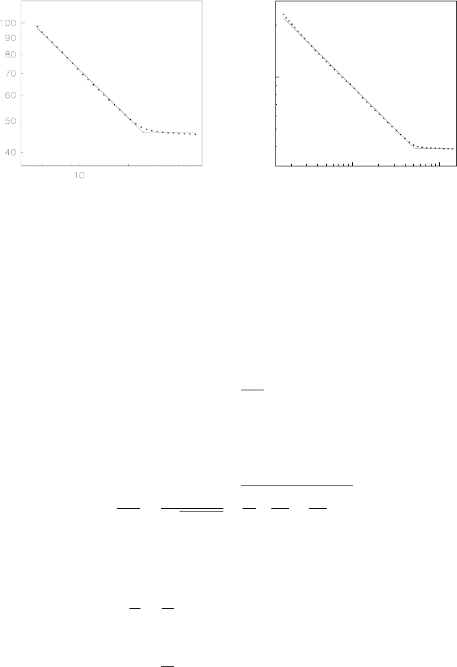
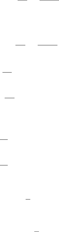
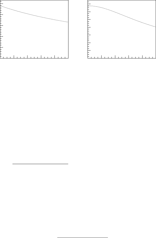
Fig. 6.3 Capacitance (in pF) curves as a function of applied voltage (in V) for two detectors of
1 cm
2
area [Leroy (1998)]: (a) resistivity of ρ = 8 kΩcm and thickness w = 247 µm; (b) resistivity
of ρ = 6 kΩcm and thickness w = 300 µm. The curve represents a fit of Eq. (6.34) to the data
points.
the negative space charge). The opposite process is observed when the applied vol-
tage decreases, leading to free charge removal and to an increase of space-charge,
Q
t
, in the transition region. The variation of Q
t
with voltage in the transition zone
has the dimension of a capacitance (C
t
), i.e.,
C
t
=
dQ
t
dV
(6.31)
with Q
t
given by
Q
t
= AqN
d
x
n
= AqN
a
x
p
. (6.32)
From the Eqs. (6.29, 6.30), one obtains
dQ
t
dV
=
Aq
2
√
V
0
+ V
b
s
2ε
q
µ
1
N
a
+
1
N
d
¶
−1
. (6.33)
Inserting Eq. (6.15) into Eq. (6.33), one recovers Eq. (6.28) describing the parallel
plate capacitor approximation, i.e., two parallel plates separated by a distance X
[C
t
and C in Eq. (6.28) being obviously the same quantity]:
C
A
=
ε
X
for 0 < X ≤ w (6.34)
and, consequently,
C = ε
A
X
for 0 < X ≤ w. (6.35)
The detector capacitance is minimal when X is maximal. This occurs when the
detector full depletion is achieved, i.e., when X = w. For applied voltage larger
January 9, 2009 10:21 World Scientific Book - 9.75in x 6.5in ws-bo ok975x65˙n˙2nd˙Ed
Solid State Detectors 461
0
0.5
1
1.5
2
2.5
3
3.5
0 20 40 60 80 100 120 140 160
V (volts)
Charge (fC)
a)
0
0.5
1
1.5
2
2.5
3
3.5
024681012
V
1/2
(volts
1/2
)
Charge (fC)
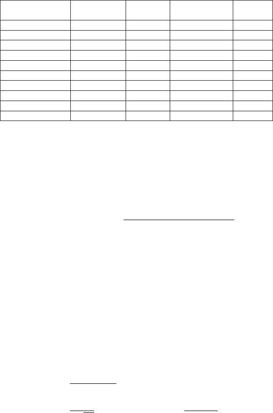
b)
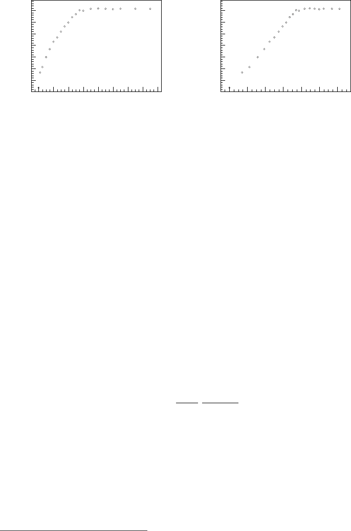
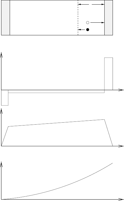
Fig. 6.4 Charge collected with a silicon detector 300 µm thick, area 1 cm
2
, exposed to incoming
electrons of energy larger than 2 MeV, as a function of the applied bias (a) and as a function of
the square root of the applied voltage (b). The value of the full depletion voltage is 60 volts which
corresponds to a collected charge of 3.5 fC, as expected from the most probable energy deposited
by relativistic electrons in this detector [Leroy (1998)].
than V
fd
, the capacitance remains constant and a plateau is observed (Fig. 6.3). An
estimate of the full depletion voltage can be obtained by taking the value of voltage
corresponding to the intersection of the C − V curve with the line of constant
geometrical capacitance. The depletion voltage decreases with increasing resistivity,
as already observed. The capacitance at full depletion of the 1 cm
2
area detectors
shown in Fig. 6.3 is obtained applying Eq. (6.28): one finds 42.5 pF [thickness
w = 247 µm, Fig. 6.3(a)] and 35.0 pF [thickness w = 300 µm, Fig. 6.3(b)].
Furthermore, the measurement of capacitance as a function of the applied
bias voltage allows the determination of the full depletion voltage and N
eff
('
V
fd
2ε/qw
2
), from Eq. (6.24) where V
0
has been neglected. As will be seen in
Sect. 6.1.4, the full depletion bias voltage can also be obtained from charge col-
lection measurements. C − V measurements permit the determination of N
eff
as
a function of the depth X of the depletion layer, i.e., the N
eff
profile. Combining
Eqs. (6.24, 6.34) (where V = V
d
+ V
0
), one finds:
N
eff
(X) =
2
qεA
2
dV
d(1/C
2
)
. (6.36)
6.1.4 Charge Collection Measurements
Let us turn to the study of the energy deposited by relativistic electrons
∗
in silicon
detectors of current use. Since these detectors are thin (a few hundreds microns,
typically), the energy deposited by minimum ionizing particles (mip) in these silicon
detectors follows a Landau-type spectrum. The most probable energy deposition by
∗
The energy deposited by relativistic electrons is similar to the energy deposited by minimum
ionizing particles (see Sect. 2.1.6.1).
January 9, 2009 10:21 World Scientific Book - 9.75in x 6.5in ws-bo ok975x65˙n˙2nd˙Ed
462 Principles of Radiation Interaction in Matter and Detection
a mip is about 80 keV per 300 µm of silicon. If one takes into account the ionization
energy E
ion
= 3.62 eV, that corresponds to about 22,000 electron-hole pairs created
per 300 µm of silicon. Then, a charge of 22, 000 ×1.6 ×10
−19
C = 3.5 fC is released
per 300 µm of silicon. An example is shown in Fig. 6.4(a) where the collected charge
as a function of the applied bias voltage is shown for a silicon detector 300 µm thick
exposed to relativistic electrons (of energy larger than 2 MeV). Figure 6.4(b) shows
the collected charge as a function of V
1/2
for the same detector exposed to the
same incoming electron beam. In agreement with Eqs. (6.22) or (6.26), it can be
observed that the detector signal (collected charge) has a square root dependence
on the bias voltage b elow the full depletion voltage and is constant (Q = 3.5 fC) as
a function of V above it. The measurement of the collected charge as a function of
the applied bias voltage is a way to determine the value of the full depletion voltage
(V
fd
), i.e., the value of voltage for which a value of the collected charge constant
with voltage begins to be observed. For the example shown is Fig. 6.4, the plateau
starts at V
fd
∼ 60 V.
The mean charge collection
†
is proportional to the detector thickness. Figure 6.5
shows the mean charge collection from relativistic electrons (E
e
> 2 MeV) for fully
depleted detectors of various thicknesses [(142–996) µm]. The average energy de-
position is ∼ (2.70 ± 0.04) × 10
2
eV µm
−1
, in agreement with the expected energy
deposition for relativistic electrons.
6.1.5 Charge Transport in Silicon Diodes
The movement of the charge carriers generated by an ionizing particle in a detector
produces a signal which shape is determined by the charge transport properties
of the detector. The charge transport properties of the diode are governed by its
electrical characteristics: i) the effective concentration of dopants (N
eff
), which
defines the internal electric field and, thus, the depletion voltage, ii) the electron
(µ
e
) and hole (µ
h
) mobilities, which influence the time needed to collect the charge
and iii) the charge trapping lifetime (τ
th
, τ
te
), which affects the efficiency of the
charge collection. First, let us assume a simplified model where the electron and
hole mobilities are constant with the electric field. The electric field inside the
depleted region of the detector can be expressed as [Lemeilleur et al. (1994)]:
E(x) = −
qN
eff
²
(x − w) +
V
b
− V
fd
w
= −ax + b, (6.37)
where V
b
is the applied bias voltage, V
fd
is the full depletion voltage,
b ≡
wqN
eff
²
+
V
b
− V
fd
w
and a =
qN
eff
²
.
Ramo’s theorem [Ramo (1939)] relates the displacement (∆x) of a charge carrier
generated by the passage of an incoming particle in the detector to the charge (∆q)
†
The reader may refer to Sects. 2.1.1, 2.1.6.1 for a further discussion.
January 9, 2009 10:21 World Scientific Book - 9.75in x 6.5in ws-bo ok975x65˙n˙2nd˙Ed
Solid State Detectors 463
0
2
4
6
8
10
12
14
0 200 400 600 800 1000
thickness (microns)
collected charge (fC)
Fig. 6.5 Mean charge collection (fC) for relativistic electrons from a
106
Ru source (with E
e
>
2 MeV) as a function of the detector thickness (142–996 µm). The line is to guide the eye (reprinted
from Nucl. Instr. and Meth. in Phys. Res. A 479, Bechevet, D., Glaser, M., Houdayer, A., Lebel,
C., Leroy, C., Moll, M. and Roy, P., Results of irradiation tests on standard planar silicon detectors
with 7–10 MeV protons, 487–497, Copyright (2002), with permission from Elsevier).
that it induces on the electro des:
∆q = q
∆x
w
. (6.38)
The induced current at the electrode is given by
i(x) =
dQ
dt
=
Q
w
dx
dt
=
Q
w
v(t), (6.39)
where
v(t) = v
e
(t) =
dx
e
dt
= µ
e
E(x) = µ
e
(−ax + b), (6.40)
for electrons, and
v(t) = v
h
(t) =
dx
h
dt
= µ
h
E(x) = −µ
h
(−ax + b) (6.41)
for holes; µ
e
and µ
h
are the electron and hole mobility, respectively. Integrating
Eqs. (6.40, 6.41) over time for a unit charge generated at x = x
0
gives
x
e
(t) =
b
a
+
µ
x
0
−
b
a
¶
exp(−µ
e
at), (6.42)
and
x
h
(t) =
b
a
+
µ
x
0
−
b
a
¶
exp(µ
h
at), (6.43)
January 9, 2009 10:21 World Scientific Book - 9.75in x 6.5in ws-bo ok975x65˙n˙2nd˙Ed
464 Principles of Radiation Interaction in Matter and Detection
with the corresponding electron and hole velocities:
v
e
(t) = −µ
e
(ax
0
− b) exp(−µ
e
at) (6.44)
and
v
h
(t) = µ
h
(ax
0
− b) exp(µ
h
at). (6.45)
The electron collection time (t
coll
), i.e., the time taken by the electron generated at
x = x
0
to reach the electrode located at x = w, is given by
t
coll
(e) = −
1
µ
e
a
ln
µ
aw − b
ax
0
− b
¶
. (6.46)
In the same way a hole collection time can defined, while the electron generated
at x = x
0
is drifting towards the electrode at x = w, the hole drifts in opposite
direction from x = x
0
to x = 0 during the time:
t
coll
(h) =
1
µ
h
a
ln
µ
−b
ax
0
− b
¶
. (6.47)
The current induced by electrons (i
e
) and holes (i
h
) at the electrodes is given by:
i
e
(t) =
qµ
e
w
(ax
0
− b) exp(−µ
e
at), (6.48)
for 0 ≤ t ≤ t
coll
(e), and
i
h
(t) =
qµ
h
w
(ax
0
− b) exp(µ
h
at), (6.49)
for 0 ≤ t ≤ t
coll
(h).
The integration of the currents over time gives the electron and hole collected
charge:
Q
e
(t) = −
q
aw
(ax
0
− b) [exp(−µ
e
at) − 1] , (6.50)
for 0 ≤ t ≤ t
coll
(e), and
Q
h
(t) =
q
aw
(ax
0
− b) [exp(µ
h
at) − 1] , (6.51)
for 0 ≤ t ≤ t
coll
(h). The total electron collected charge is obtained by integrating
Eq. (6.50) over time
Q
tot
(e) =
q
w
(w − x
0
), (6.52)
while the total hole collected charge is obtained from the integration of Eq. (6.51)
over time:
Q
tot
(h) =
q
w
x
0
. (6.53)
Summing Eqs. (6.52, 6.53), we get a total collected charge of
Q
tot
= q, (6.54)
i.e., the unit charge initially injected.
January 9, 2009 10:21 World Scientific Book - 9.75in x 6.5in ws-bo ok975x65˙n˙2nd˙Ed
Solid State Detectors 465
n+
(x)
p+n
Back Front
0w
r
h
e
XX
min max
X
0
E(x)
X
X
ρ
− ψ (x)
a)
b)
c)
d)
Fig. 6.6 (a) Representation of a p
+
− n −n
+
dio de (over-depleted), (b) the dopant density
profile ρ, (c) the electric field E and (d) the electrostatic potential ψ (reprinted from Nucl.
Instr. and Meth. in Phys. Res. A 479, Bechevet, D., Glaser, M., Houdayer, A., Lebel,
C., Leroy, C., Moll, M. and Roy, P., Results of irradiation tests on standard planar sili-
con detectors with 7–10 MeV protons, 487–497, Copyright (2002), with permission from
Elsevier).
A more complete treatment of the charge transport problem is presented be-
low. In that case, the mobility will be expressed as a function of the electric field
and of other parameters. A planar silicon diode (p
+
−n − n
+
) is assumed with the
junction and ohmic side located at x = 0 et x = w, respectively. Figure 6.6 gives a
schematic view of the junction under consideration. These electrical characteristics
January 9, 2009 10:21 World Scientific Book - 9.75in x 6.5in ws-bo ok975x65˙n˙2nd˙Ed
466 Principles of Radiation Interaction in Matter and Detection
are extracted by solving in one-dimension (through the use of a transverse diffusion
term) a system of five partial differential equations with space (x) and time (t)
variables ([Leroy, Roy, Casse, Glaser, Grigoriev and Lemeilleur (1999a)] for more
details). A single trap state is assumed. Equation (6.7) is rewritten as:
∇
2
ψ = −∇E = −
q
ε
(−N
eff
− n + p − n
t
+ p
t
), (6.55)
n (p) is the free electron (hole) density while n
t
(p
t
) is the trapped electron (hole)
density. The difference p − n in Eq. (6.55) accounts for possible plasma effects,
when the electron and hole densities are of the order of the effective concentration
of dopants. The carriers are thus shielding themselves from the external electric
field and take a longer time to be collected.
500
600
700
800
900
1000
1100
1200
1300
0123456
dE⁄dx (MeV cm
2
g
-1
)
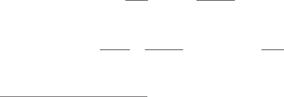
Fig. 6.7 Energy deposition of an alpha-particle in silicon (reprinted from Nucl. Instr. and Meth.
in Phys. Res. A 479, Bechevet, D., Glaser, M., Houdayer, A., Lebel, C., Leroy, C., Moll, M. and
Roy, P., Results of irradiation tests on standard planar silicon detectors with 7–10 MeV protons,
487–497, Copyright (2002), with permission from Elsevier).
The system of equations involves two continuity equations for electrons and
holes:
∂n
∂t
= −
∂n
t
∂t
+
∇J
n
q
+ g − Rn − U
SRH
,
∂p
∂t
= −
∂p
t
∂t
−
∇J
p
q
+ g − Rp − U
SRH
, (6.56)
∂n
t
∂t
=
n
τ
te
−
p
t
τ
de
− Rn
t
,
∂p
t
∂t
=
p
τ
th
−
p
t
τ
dh
− Rp
t
, (6.57)
where g is the electron–hole pair generation function, τ
te/h
and τ
de/h
are the
trapping and de-trapping times, respectively; U
SRH
is the Shockley–Read–Hall
generation-recombination term
U
SRH
=
np − n
2
int
(p + n
int
)τ
th
+ (n + n
int
)τ
te
. (6.58)
The current densities of carriers densities are given by:
J
n
= qnµ
e
E + µ
e
k
B
T ∇n,
J
p
= qpµ
h
E − µ
h
k
B
T ∇p, (6.59)
January 9, 2009 10:21 World Scientific Book - 9.75in x 6.5in ws-bo ok975x65˙n˙2nd˙Ed
Solid State Detectors 467
where k
B
and T are the Boltzmann constant and the temperature, respectively; µ
e
and µ
h
are the electron and hole mobilities, respectively. These mobilities depend
on the electric field (E) and the temperature (T ). The system of equations reflects a
cylindrical symmetry as the induced charges are generated inside a cylinder and are
transversely diffused with time. In Eqs. (6.56, 6.57), this is accounted by the term
R [Taroni and Zanarini (1969)], which takes into account the transverse diffusion
of charge carriers:
R =
18D
a
18D
a
t + r
2
0
, (6.60)
where r
0
is the initial radius of the column of deposited charge, the radius of the
column at a time t b eing
r
2
(t) = 18 D
a
t + r
2
0
;
D
a
is the ambipolar diffusion coefficient and can be expressed as
D
a
=
2D
e
D
h
D
e
+ D
h
, (6.61)
where
D
c
=
kT
q
µ
c
(6.62)
are the Einstein relations (c = e, h). Values of the diffusion coefficients, D
c
(c =
e, h), are given at page 487. It has to be noted that the minority carrier diffusion
length for electrons in p-type material is given by
L
e
=
p
D
e
τ
e
(6.63)
and for holes in n-type material is given by
L
h
=
p
D
h
τ
h
, (6.64)
where τ
e
and τ
h
are the electron and hole carrier lifetime, respectively.
When neglecting the size of the p
+
and n
+
regions, the integration of the one-
dimensional Poisson’s equation at t = 0, for a simple abrupt p−n junction operated
in over-depleted mode (V
b
> V
fd
), gives
E(x, 0) = −
qN
eff
²
x +
V
b
w
+
V
fd
N
eff
w |N
eff
|
, for 0 < x < w (6.65)
with the boundary conditions:
E(0, t) = E(w, t) = 0, (6.66)
ψ(0, t) = V
0
+ ψ
p
≈ 0 and ψ(w, t) = ψ
p
− V
b
≈ −V
b
, (6.67)
where ψ and E are the electrostatic potential and the electric field, respectively; q,
² and w are the electrical charge, the silicon electric permittivity and the thickness
of the diode, respectively; V
0
≈ 0.6 V is the built-in voltage, V
b
is the applied bias
January 9, 2009 10:21 World Scientific Book - 9.75in x 6.5in ws-bo ok975x65˙n˙2nd˙Ed
468 Principles of Radiation Interaction in Matter and Detection
0
100
200
300
400
500
0246810
Electric field (kV/cm)
Holes mobility (cm
2
/Vs)
0
200
400
600
800
1000
1200
1400
0246810
Electric field (kV/cm)
Electrons mobility (cm
2
/Vs)
Fig. 6.8 Hole (left) and electron (right) mobility (cm
2
V
−1
s
−1
) as a function of the electric field
(kV/cm), Eq. (6.69), (reprinted from Nucl. Instr. and Meth. in Phys. Res. A 479, Bechevet,
D., Glaser, M., Houdayer, A., Lebel, C., Leroy, C., Moll, M. and Roy, P., Results of irradiation
tests on standard planar silicon detectors with 7–10 MeV protons, 487–497, Copyright (2002), with
permission from Elsevier).
voltage, ψ
p
(−0.6 ≤ ψ
p
≤ −0.3 V) is the electrostatic potential of the neutral p-type
region and V
fd
is the full depletion bias voltage.
For a relativistic β particle in silicon, the range exceeds the physical size of
the detector and a uniform density of electron–hole pairs is created with n
0
≈
80 pairs/µm.
The generation function, g in Eq. (6.56, 6.57) at time t = 0 is given by:
g(x) =
n
0
× density(x) δ(x − x
0
)
P
x
0
density(x
0
)
with x
min
≤ x
0
≤ x
max
. (6.68)
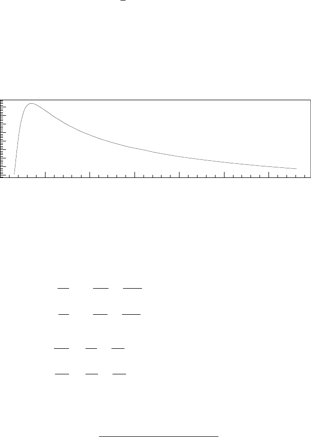
For an α particle of 5.0 MeV in silicon, the number of electron–hole pairs created
is n
0
≈ 1.4 million pairs over a range
r = x
max
− x
min
≈ 25 µm,
while the density of the electron–hole pairs is obtained by interpolation of the data
from [Williamson, Boujot and Picard (1966)] shown in Fig. 6.7.
The drift velocity of the charge carrier reaches a saturation value v
s
for elec-
tric field values around 10
4
V/cm [Dargys and Kundrotas (1994)]. The empirical
equation describing the mobility as a function of the electric field is:
µ(x) =
µ
0
[1 + (µ
0
E(x)/v
s
)
m
]
1/m
, (6.69)
where µ
0
is the zero field mobility, m = 1 for holes, m = 2 for electrons; v
s
=
1.05×10
7
and 10
7
cm/s for electrons and holes, respectively [Dargys and Kundrotas
(1994)]. The dependence of the mobilities on the electric field is shown in Fig. 6.8
for holes (left) and electrons (right).
January 9, 2009 10:21 World Scientific Book - 9.75in x 6.5in ws-bo ok975x65˙n˙2nd˙Ed
Solid State Detectors 469
Table 6.1 Examples [Leroy, Roy, Casse, Glaser, Grigoriev and Lemeilleur
(1999a); Roy (2000)] of characteristics of the standard planar silicon detectors
of current use.
Detector Current thickness |N
eff
| ρ
(area) pulse source (µm) (×10
11
cm
−3
) (kΩ cm)
M4 (1 cm
2
) α 317 3.4 12.2
M18 (1 cm
2
) α,β 309 4.1 11.0
M25 (1 cm
2
) α,β 308 2.1 23.0
M35 (1 cm
2
) α 508 1.7 24.0
M49 (1 cm
2
) β 301 4.7 8.9
M50 (1 cm
2
) β 471 1.8 22.8
M53 (1 cm
2
) β 223 5.4 7.7
P88 (0.25 cm
2
) α,β 290 18.0 2.5
P189 (0.25 cm
2
) α,β 294 18.0 2.5
P304 (0.25 cm
2
) α,β 320 7.0 6.0
The mobilities also depend on the temperature and dopant concentra-
tions [Caughey and Thomas (1967)]. The effect of concentration is only appreciable
for concentrations over 10
14
dopants/cm
3
. Changing the temperature by 1.5 degree
Celsius changes both mobilities by ≈ 1%. These features are taken into account via
the empirical equation
µ(T, N
eff
) = µ
min
+
µ
0
(T/300)
ν
− µ
min
1 + (T /300)
ξ
(N
eff
/N
ref
)
α
, (6.70)
where the values used for the electrons (holes) are: µ
min
= 55.24 (49.7) cm
2
V
−1
s
−1
,
N
ref
= 1.072 × 10
17
(1.606 × 10
17
) dopants/cm
3
, ν = −2.3 (−2.2), ξ = −3.8
(−3.7), α = 0.73 (0.70), T is the temperature in kelvin and µ
0
is the mobility at
T = 300 K. The temperature dependence of mobility is shown in Fig. 6.9 using
µ
0
(for e) = 1350 cm
2
V
−1
s
−1
and µ
0
(for h) = 480 cm
2
V
−1
s
−1
at T = 300 K.
As a consequence of Ramo’s theorem [Eq. (6.38)], the observed signal, V (t), is a
convolution of the current, I(t), produced by all the individual charge carriers and
the response from the system, which is simply an RC circuit. The response of the
system is a Gaussian with a characteristic time constant σ = R
a
C, where C is the
capacitance of the detector and R
a
the input impedance of the amplifier:
I(t) =
18D
a
t + r
2
0
w r
2
0
Z
w
0
(µ
e
n + µ
h
p)E dx, (6.71)
V (t) =
GR
a
σ
√
2π
X
e,h
Z
∞
−∞
I(t
0
) exp
·
−
(t − t
0
)
2
2σ
2
¸
dt
0
, (6.72)
where D
a
is the ambipolar diffusion constant [Eq. (6.61)], G the gain of the amplifier
and r
0
the initial radius of the column of deposited charge.
As an example, a simple case will be examined where silicon diodes are exposed
to electrons from a
106
Ru source with an energy > 2 MeV, selected by an external
trigger, and to α-particles from an
241
Am source with an energy of 5.49 MeV. The
setup for measuring the charge induced by the charge carriers generated by
106
Ru