Martienssen W., Warlimont H. (Eds.). Handbook of Condensed Matter and Materials Data
Подождите немного. Документ загружается.

992 Part 5 Special Structures
Table 5.2-5 Reconstruction and relaxation of semiconductors, cont.
Crystal Face Reconstruction Preparation Model Remarks
symmetry
InAs (110) 1×1 Same as above Same as above
InSb (110) 1×1 Same as above Same as above
CdS (0001)Cd 1×1 IBA
CdSe (10
¯
10) 1×1 Cleaving Rotation/relaxation Results controversial
(Fig. 5.2-17, Table 5.2-8)
ZnO (0001)Zn 1×1 Cleaving, IBA
placements of atoms that conserve the lengths of the
bonds but not their relative angles.
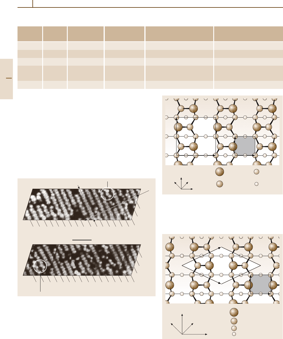
Figures 5.2-7 – 5.2-17 give the accepted recon-
struction models for a selection of covalent and
polar semiconductors, together with STM (scan-
ning tunneling microscopy) images of some of the
surfaces. Tables 5.2-6, 5.2-7, and 5.2-8 give the
positions of the atoms in reconstructed Si(111)
2 × 1 and Si (111)7 ×7 surfaces and the param-
eters of the rotation/relaxation model of polar
semiconductors.
17
18
19
<110>
1a 2 3 4 5 6 7 8 9 10 11 12 13 14 15 16
1A
A
B
p(2× 2)
25 Å
1b 2 3 4 5 6 7 8 9 10 11 12 13 14 15
1B
c(4× 2)
17
19
18
16
Fig. 5.2-9 STM image of the Si(100) surface showing coexistence
of 2 × 1, p(2× 2), and c(4× 2) reconstructions [2.20]
Fig. 5.2-10 Ordered arrangement of buckled dimers that
gives rise to c(4× 2) reconstruction of the (100) face of Si
and Ge (top views). Ideal (shaded) and reconstructed unit
cells are shown
1st layer,
upper atoms
1st layer,
lower atoms
2nd layer
3rd layer
B
A
b
a
[110]
[010][1
–
00]
[1
–
10]
Fig. 5.2-8 Ordered arrangement of buckled dimers that
gives rise to p(2 ×2) reconstruction of the (100) face of
Si and Ge (top views). Ideal (shaded) and reconstructed
unit cells are shown
1st layer, upper atoms
[110]
[010][1
–
00]
[1
–
10]
1st layer, lower atoms
2nd layer
3rd layer
B
A
b
a
Part 5 2.2
The Physics of Solid Surfaces 2.2 Surface Reconstruction and Relaxation 993
1st layer, upper atoms
1st layer, lower atoms
2nd layer
3rd layer
[1
–
01]
[1
–
10]
[01
–
1]
a)
B
A
b
a
[2
–
11]
[111]
1
2
4
6
7
5
3
8
b)
Table 5.2-6 Coordinates of the atoms of the uppermost
layers of Si(111) 2 ×1 (π-bonded chain geometry). The
atoms are labeled as in Fig. 5.2-11b. The origin is at atom 1;
the XYZ axes are in the directions [
¯
1
¯
1
¯
1], [1
¯
10], and [
¯
1
¯
12],
respectively
1
Atom X (Å) Y (Å) Z (Å)
1 0.0 0.0 0.0
2 0.34 1.92 1.12
3 1.32 0.0 −1.98
4 1.23 1.92 3.28
5 3.51 0.0 −1.14
6 3.40 1.92 2.35
7 4.09 0.0 1.16
8 4.35 1.92 −2.18
1
Data are average values from various authors.
References to the original papers are given in [2.3]
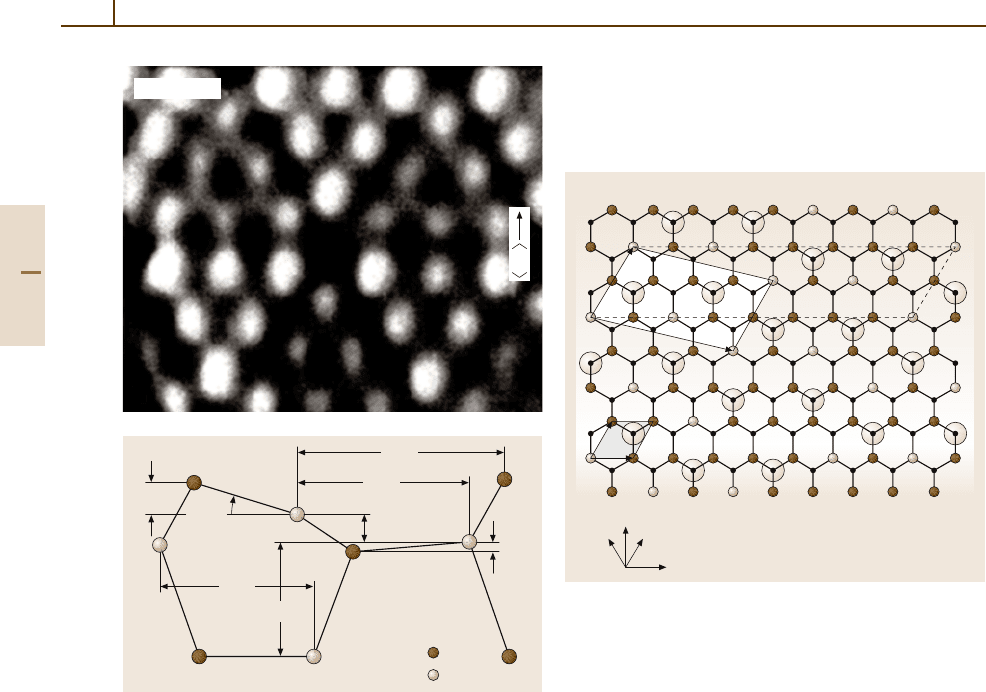
Fig. 5.2-11 (a) top view and (b) side view of the Pandey’s
π-bonded chain model for the 2 ×1 reconstruction of the
(111) face of diamond, Si and Ge [2.21]. In
(a) the ideal
(shaded) and 2×1 unit cells are shown. The numeration of
atoms in
(b) refers to the positions given in Table 5.2-6
10Å
2Å
[01
-
1
-
]
[21
-
1
-
]
Fig. 5.2-12 STM image of Si(111) 2×1, showing the great
anisotropy of the surface, in agreement with the model of
Fig. 5.2-11. Optical SDR spectra (see Fig. 5.2-41) show the
same anisotropy [2.22]
Part 5 2.2
994 Part 5 Special Structures
[2
–
11]
[1
–
01]
[01
–
1]
[2
–
11]
[111]
a)
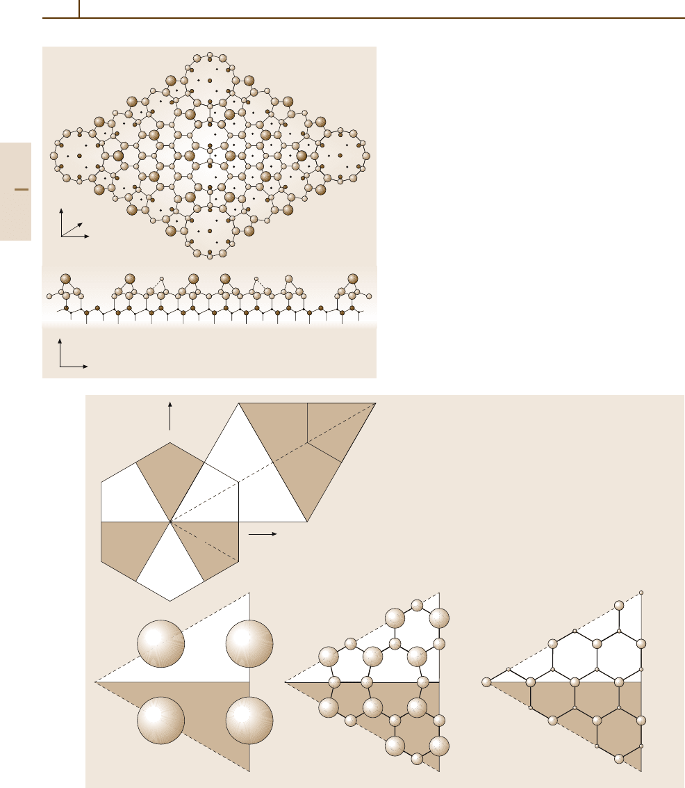
b)
Si(111) 7 × 7
104
3
1
2
4
A
B
106
A
112
109
116
B
107
124
120105
119118117 119
126125
121
110
115
108
114
103
111
113
122 123
17
18
24
23
22
21
33
32
31
20
15
26
28 25
29
27
13
14
30
15
16
A
B
b) c)
d)
a)
B
D
C
F
E
F
A
E
D
C
x
y
B
Fig. 5.2-13a,b DAS (dimers, adatoms, and stacking faults)
+ vacancy model of Takayanagi et al. for Si(111) 7 ×7.
(a) Top view; (b) side view. In (a), the unit cell could be
drawn by joining the centers of the four vacancies. The
faulted area is the triangular half-cell on the left. The rota-
tion associated with the stacking fault hides atoms in deep
unreconstructed layers, which, in contrast, are visible in the
unfaulted right-hand side [2.23]
Fig. 5.2-14a–d Symmetry-reduced unit cell for Si(111)
7×7(DASmodel).In
(a), the unit cell (two triangular
halves, one faulted (hatched) and one unfaulted) is reduced
to smaller subunits and recomposed into a c-hexagonal
cell. The atoms are drawn and numbered in
(b)–(d).The
numbering is the same as in Table 5.2-7; the origin of the
coordinates is at atom 103.
(b) The four adatoms; (c) the
first- and second-layer atoms;
(d) the third- and fourth-layer
atoms [2.24,25]
Part 5 2.2
The Physics of Solid Surfaces 2.2 Surface Reconstruction and Relaxation 995
Table 5.2-7 Coordinates of the adatoms and four uppermost layer atoms in the symmetry-reduced unit cell of Si(111)
7× 7 (see Fig. 5.2-14 for the numbering of the atoms). The origin is taken at atom 103
1
.X-raydatagiveavalueof2.11 Å
for the adatom–back atom projected bond length (between atoms 1 and 13 and between atoms 1 and 28 in the table) and
a value of 2.49 Å for the dimer bond length (betweens atoms 26 and 27 in the table) [2.24–26]
Atom no. x (Å) y (Å) z (Å) Atom no. x (Å) y (Å) z (Å)
1 5.76 3.33 −4.21 103 0.00 0.00 −0.05
2 13.44 3.33 −4.17 104 13.44 7.76 0.73
3 5.76 −3.33 −4.29 105 5.76 3.33 0.45
4 13.44 −3.33 −4.25 106 13.44 3.33 0.45
13 4.01 2.32 −2.94 107 11.52 6.65 −0.07
14 5.76 3.33 −1.68 108 5.76 −3.33 0.45
15 9.60 5.54 −3.11 109 13.44 −3.33 0.45
16 11.55 6.67 −2.41 110 11.52 −6.65 −0.07
17 13.44 5.32 −2.98 111 1.92 1.11 0.74
18 13.44 3.33 −1.68 112 13.44 1.11 0.87
19 4.01 −2.32 −2.99 113 7.68 4.43 0.80
20 5.76 −3.33 −1.73 114 3.84 −2.22 0.85
21 9.60 −5.54 −3.16 115 9.60 −5.54 0.73
22 11.55 −6.67 −2.46 116 13.44 −5.54 0.80
23 13.44 −5.32 −3.03 117 3.84 0.00 0.00
24 13.44 −3.33 −1.73 118 7.68 0.00 0.00
25 12.21 0.00 −2.24 119 11.52 0.00 0.00
26 6.98 0.00 −2.24 120 9.60 3.33 −0.07
27 4.53 0.00 −2.24 121 9.60 −3.33 −0.07
28 7.49 2.33 −2.98 122 5.76 1.11 0.87
29 11.71 2.33 −2.98 123 9.60 1.11 0.72
30 9.60 3.29 −2.41 124 11.52 4.43 0.80
31 7.49 −2.33 −3.03 125 7.68 −2.22 0.83
32 11.71 −2.33 −3.03 126 11.52 −2.22 0.83
33 9.60 −3.29 −2.46
1
A table of the atomic positions for the full 7×7 cell is given in [2.25]. The results were obtained by LEED analysis [2.24]
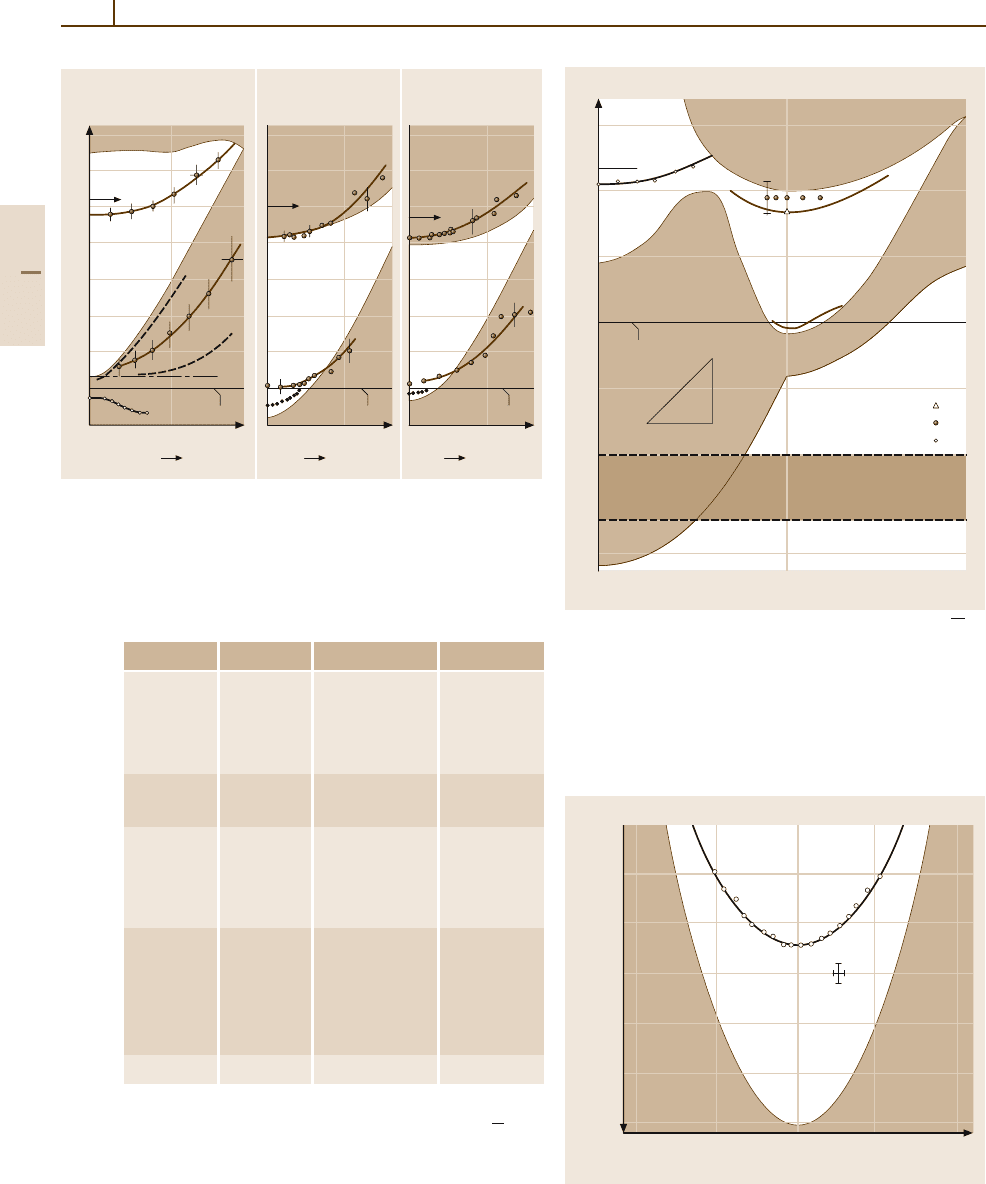
Table 5.2-8 Surface relaxation and rotation parameters for polar semiconductors as defined in Fig. 5.2-17
1
Crystal ω(
◦
) ∆
1⊥
(Å) ∆
2⊥
(Å) ∆
1y
(Å) d
12⊥
(Å) d
12y
(Å) d
23⊥
(Å)
GaAs 27.4 0.65 −0.12 4.39 1.43 3.31 2.06
GaP 27.5 0.63 0.0 4.24 1.44 3.20 1.93
GaSb 30 0.77 0.0 4.79 1.61 3.27 2.16
InAs 36.5 0.78 −0.15 4.98 1.50 3.60 2.21
InP 28 0.69 0.0 4.57 1.59 3.45 2.07
InSb 28.8 0.78 −0.18 5.06 1.60 3.82 2.38
CdSe 21.3 1.03 0.0 4.60 0.45 4.10 2.48
1
The data were obtained by dynamical LEED analysis. References to the original papers are given in [2.3,4]
Part 5 2.2
996 Part 5 Special Structures
Si(111) 7 × 7
112
–
∆
2, ⊥
∆
1, y
∆
1, ⊥
ω
d
12, ⊥
d
12, y
d
23, y
d
23, ⊥
Cation
Anion
Side view
Fig. 5.2-17 Side view of the relaxed cell of a GaAs-type
crystal, with parameters occurring in the relaxation/rotation
model of the (110) face used in Table 5.2-8
Fig. 5.2-15 STM image of the Si(111)7 × 7 surface. The
picture gives evidence to the 12 adatoms, the 4 vacancies,
and the asymmetry between the two triangular half cells of
Fig. 5.2-13 [2.7,27]
Ge(111) c(2 × 8)
a
b
B
A
[11
–
0]
[101
–
][011
–
]
[112
–
]
Fig. 5.2-16 Top view of Ge(111)c(2 × 8) simple adatom
model. Large and small empty circles represent adatoms
and “rest” atoms respectively. Both ideal (shaded)and
c(2× 8) unit cells are shown [2.28]
5.2.3 Electronic Structure of Surfaces
The truncation of the lattice and/or the reconstruction
and relaxation cause the electronic states at the surface
or in the uppermost layers to be distinctly different from
those of the bulk. Such new states are called surface
states. Their wave functions decay exponentially on both
sides of the surface. Since their k
⊥
is imaginary, the sur-
face band structure is defined in the surface Brillouin
zone (SBZ), which is the projection of the 3-D Brillouin
zone onto the surface plane. The projection of the bulk
bands onto the SBZ is called the projected band struc-
ture. When the energy of a surface state is localized in
a gap of the projected bulk structure (either an absolute
gapp, i. e. one that extends throughout the whole SBZ,
or a partial gap), one speaks of a true (or bona fide)
surface state. When there is degeneracy (both in energy
and k) with the bulk bands, one speaks of a surface
resonance.
The SBZs, of the most common faces of fcc and bcc
crystals are shown in Fig. 5.2-18.
The potential felt by an electron outside the surface
(though sufficiently far from it) is the classical image
potential: (−e
2
/4z)(ε −1)/(ε +1), ε being the dielec-
tric function of the crystal. From a microscopic point of
view, the image potential arises from the charge density
fluctuations induced in the solid by the outside electron.
An important consequence of the Coulomb-like image
potential is the occurrence ofimage states in the potential
well outside the solid (especially in metals). In surface
structure calculations done with the local-density ap-
proximation (LDA), such image states are not present,
Part 5 2.3
The Physics of Solid Surfaces 2.3 Electronic Structure of Surfaces 997
[21
–
1
–
]
[011
–
]
[12
–
1]
[011]
[001
–
]M
––
X
––
Γ
–
Γ
–
X
––
S
–
Y
––
[001]
[1
–
10]
fcc (100) fcc (110)
fcc and bcc (111) bcc (100)
M
––
M
––
'
K
––
Γ
–
[010]
[011]M
––
X
––
Γ
–
Fig. 5.2-18 Surface Brillouin zones of fcc (100), (110), and
(111), bcc (100) and (111) faces
since the potential decays exponentially on the vacuum
side. Nonlocal forms of the exchange correlation ener-
gies that give the correct long-range potential have been
introduced to overcome this difficulty.
Surface states were first detected by optical tech-
niques in semiconductors and are now studied mainly
by ARUPS, KRIPES, STM, SDR, and reflectance
anisotropy spectroscopy (RAS).
Data, in the form of tables and figures, are presented
separately for metals (including jellium), semiconduc-
tors, and magnetic surfaces.
5.2.3.1 Metals
The data are ordered alphabetically according to the
chemical symbol. Where necessary, introductory re-
marks are given. A more detailed discussion is given
in [2.9,11].
Work Function Data
Work function data are listed in Table 5.2-9 with the
specification of the method of measurement.
Table 5.2-9 Work functions Φ of metals (average values
from various authors; references to the original papers are
given in [2.9, 16]). P, photoelectric threshold; A, angle-
resolved photoemission spectroscopy; T, thermionic emis-
sion; F, field emission; th, theory
Metal Face Φ(eV) Technique
Ag
(100) 4.18 P
4.38 A
4.2 th
(111) 4.46 P
4.50 A
Al
(100) 4.30 P
(110) 4.17 P
(111) 4.23 P
4.5 th
Au
(100) 5.22 A
(110) 5.20 A
(111) 5.26 A
Co (0001) 5.2 A
Cu
(100) 4.59 P
4.63 A
5.10 F
4.5 th
(110) 4.48 P
4.5 A
(111) 4.85 P
4.5 A
Fe
(100) 4.67 P
(110) 5.05 A
(111) 4.81 P
Ir
(110) 5.42 F
(111) 5.76 F
Mo
(100) 4.53 P
(110) 4.95 P
(111) 4.55 P
Ni
(100) 4.89 T
5.53 F
5.1 th
(110) 4.64 T
(111) 5.22 T
Pb (111) 4.05 A
Pd
(111) 5.58 A
5.8 th
Pt
(100) 5.84 P
5.84 F
(111) 5.82 A
5.93 F
Rh
(100) 5.1 th
(111) 5.35 th
Ta
(100) 4.15 T
(110) 4.80 T
(111) 4.00 T
W
(100) 4.66 F
4.5 th
(110) 5.57 F
(111) 4.46 F
Part 5 2.3
998 Part 5 Special Structures
Surface Core Level Shifts (SCLS)
A shift in the energy of the core levels is caused by
charge transfer between surface and bulk atoms. A posi-
tive SCLS means a larger binding energy. It is generally
assumed that in metals the change in the width of the
band and its position with respect to the Fermi energy are
the important factors. Data are shown in Table 5.2-10.
Jellium Model
The jellium model of a metal surface takes into account,
in a simplified though significant way, the problem of
electron–electron interaction. The atomic potential is
smeared out into a uniform positive background extend-
ing over the region z ≤ 0. The electron density is taken
into account by a dimensionless parameter r
s
,defined
by the equation
(4/3)π(r
s
a
0
)
3
n =1 ,
where a
0
is the Bohr radius and n the bulk electron
density.
Figure 5.2-19 shows the charge density as a function
of z for r
s
= 2 and r
s
= 5, corresponding roughly to
Al and K. Table 5.2-11 gives the values of the work
function Φ for various values of r
s
and compares the
Table 5.2-10 Surface core level shift data. The data are from various authors. References to the original papers are given
in [2.9]
Metal Surface Core level SCLS (eV) Remarks
Al
(100)
2p
−0.057 Photoemission (partial yield)
−0.120 Theory
(110) and (111) 0.0 UPS
Au
(100) 1× 1
4f
−0.35 UPS
(100) 5×20 −0.28 UPS
(111) −0.35 UPS, no distinct results for (111) 23 × 1
Cu
(100) 3s −0.36 Theory
2p −0.27 UPS
Ir
(100) 1× 5
4f
−0.49
(111) −0.50
Pt
(110) 1× 2
4f
−0.21 UPS, evidence for nonequivalent atoms
−0.55
(111) −0.40 UPS
Rh
(100)
4d
−0.75 1st layer Theory
−0.05 2nd layer
(111) −0.46 1st layer
−0.05 2nd layer
W
(110)
4f
−0.30 UPS
−0.30 1st layer Theory
−0.02 2nd layer
n/n
_
z (2π/k
F
)
1.0
1.00
0.75
0.50
0.25
0
– 1.0 – 0.5 0 0.5
r
s
= 5
r
s
= 2
Positive
background
Fig. 5.2-19 Charge density near a jellium surface, for
r
s
= 2andr
s
= 5 as a function of z [2.29]
Part 5 2.3
The Physics of Solid Surfaces 2.3 Electronic Structure of Surfaces 999
Table 5.2-11 Work functions for the jellium model. Refer-
ences to the original papers are given in [2.9]
r
s
Φ
jellium
(eV ) Element Φ
exp
(eV )
2 3.89 Al (r
s
= 2.08) 4.25
2.5 3.72
3 3.50 Ag (r
s
= 3.02) 4.35
3.5 3.26
4 3.06 Na (r
s
= 3.93) 2.45
4.5 2.87
5 2.73 K(r
s
= 4.86) 2.3
results with experimental values for metallic elements
of comparable densities. Figure 5.2-20givessome useful
insight into the problem of the potential near a metallic
surface.
Image States
Image states are confined to the region of space between
the crystal surface and the image potential which de-
scribes the electrostatic force acting on an electron close
to the surface. Figure 5.2-21 illustrates the occurrence
of image states in Ag(100). The figure shows (i) the
electron potential inside and outside the crystal, (ii) the
image state levels n = 1 and n = 2 and the correspond-
ing wave functions, and (iii) the bulk band structure
E (arb. units)
z (2π/k
F
)
– 1.0
1.0
0.12
0.08
0.04
0
– 0.04
– 0.08
– 0.5 0 0.5
E
Φ
r
s
= 5
E
F
V
eff
Fig. 5.2-20 Effective one-electron potential V
eff
(contin-
uous line) and its electrostatic part (dashed line) near
a jellium surface for r
s
= 5. Notice the characteristic os-
cillations (Friedel oscillations) [2.29]
E
E
vac
= 0
0.4
0.3
0.2
0.1
0
10 15 20 25 30
z (Å)
ΓX
Ψ
n
–12
κ
2∆
∆
d
E
F
z
0
Potential
VacuumΨ
n = 1
Ψ
n = 2
ε
n = 1
= – 0.81 eV
ε
n = 2
= – 0.19 eV
Interplanar spacing
Bulk
Ag(100)
Fig. 5.2-21 Schematic drawing of energy versus distance at the sur-
face of Ag(100), illustrating the origin of the image states. Wave
functions for n = 1andn = 2 are also displayed in the right part
of the figure, corresponding to the levels in the potential well. On
the left side of the figure the bulk energy bands as a function of k
are also shown. Notice that the image state energies occur in the
band gap of the bulk. This allows confinement of the image state
electron [2.30, 31]
with an energy gap of width 2∆. It can be seen that
the image state levels have energies corresponding to
the bulk gap so that the electron cannot penetrate the
crystal [2.32].
Figure 5.2-22 shows the dispersion curves E(k
)
for the (111) faces of Ni, Cu, and Ag. Image states
(S
1
) and surface and resonance states (S
2
,S
3
),to-
gether with the projected bulk bands (hatched regions),
are shown. Table 5.2-12 gives average values of the
binding energies E
b
(measured downward from the vac-
uum level) and effective masses m
∗
/m
0
for some image
states.
Surface Dispersion Curves E(k
)
Dispersion curves are given as a function of k
along
symmetry lines of the SBZ in Figs. 5.2-23 – 5.2-30.
Where possible, a comparison with theoretical results
and the projected bulkband structure has been presented.
Most of the experimental data were obtained by
ARUPS (for filled states) and KRIPES (for empty
states). Since the component k
is conserved across the
Part 5 2.3
1000 Part 5 Special Structures
E (eV)
0.5
7
6
5
4
3
2
1
0
–1
1.00 0.5 0.500
(Å
–1
)
Γ
–
(Å
–1
)(Å
–1
)
Γ
–
Γ
–
k M
––
'
M
––
'
M
––
'
⎮⎮
k
⎮⎮
k
⎮⎮
E
vac
E
vac
E
F
S
2
B
S
1
E
F
E
F
S
3
S
1
S
2
S
1
E
vac
S
2
Ni(111) Cu(111) Ag(111)
Fig. 5.2-22 Dispersion curves E(k
) for the empty states of the
(111) face of Ni, Cu and Ag, showing image states (S
1
), surface
states and resonances (S
2
,S
3
). Experimental data by KRIPES [2.33]
Table 5.2-12 Image state parameters. The data are from
various authors. References to the original papers are given
in [2.9]
Crystal Face E
b
(eV ) m
∗
/m
0
Ag
(100) 0.51 1.32
0.16 (n = 2)
(111) 0.69 1.35
0.23 (n = 2)
Au
(100) 0.63 1.0
(111) 0.42
Cu
(100) 0.65 1.13
0.18 (n = 2)
(110) 0.48
(111) 0.82 1.07
Ni
(100) 0.4 1.2
(110) 0.6 1.7
(111) 0.74 1.3
0.25 (n = 2)
0.10 (n = 3)
Pt (111) 0.63
Fig. 5.2-25 Energydispersion curves E(k
) around Γ point
of the SBZ for Ag(111). Experimental data from ARUPS
are fitted with a parabolic band with m
∗
/m
0
= 0.53 [2.36]
E (eV)
Γ
–
M
––
X
––
6
4
2
0
–2
–4
–6
d band
Γ
–
X
––
M
––
Ag(100)
E
vac
A
E
F
B
1
2
3
Fig. 5.2-24 Energy dispersion curves E(k
) around Xof
the SBZ for Ag(100). Projected bands and surface state fea-
tures A and B are the same as in Fig. 5.2-8a. Experimental
points are obtained by: electroreflectance (1) and KRIPES
(2 and 3). Curve (3) represents image states [2.34,35]
E
F
= 0
– 0.2
0.05
0.10
0.15
0.20
0.25
0.30
E
B
(eV)
– 0.1 0 0.1 0.2
k
⎮⎮
(Å
–1
)
Γ
–
SS Ag(111)
Part 5 2.3
The Physics of Solid Surfaces 2.3 Electronic Structure of Surfaces 1001
Fig. 5.2-23 Theoretical projected band structures (shaded
areas) along symmetry lines of the SBZ for Ag(100),
Ag(110) and Ag(111). Surface states (solid lines)and
resonances (dashed lines) are shown. SBZ in the in-
sets [2.37–39]
surface, the determination of the direction of the emitted
or incident electron in ARUPS or KRIPES, respectively,
and its energy allows the determination of the dispersion
curve through the relation
k
= (2mE
kin
/
2
)
1/2
sin θ,
where E
kin
is the kinetic energy of theemitted or incident
electron and θ the angle of emission or incidence with
respect to the surface normal.
Because of the large amount of data available for
metals, only a few significant examples have been given.
For more detailed information, the reader is referred
to [2.9, 11].
Surface Plasmons
Surface plasmons are self-sustained oscillations that de-
cay exponentially on both sides of the surface plane.
They occur at the poles of the loss function, i. e. for
ε
1
= 0inthebulkandε
1
=−1 at the surface, ε
1
be-
ing the real part of the dielectric function. The surface
plasmon is shifted to lower energies with respect to the
bulk.
Table 5.2-13 gives some of the parameters of surface
plasmons for various metals. d
⊥
(ω) is, in the jellium
model, the distance of the centroid of the induced charge
from the surface plane. d
⊥
> 0 means that the centroid
is outside the edge of the jellium. Figure 5.2-31 shows
the dispersion curves of surface plasmons for Al(111).
For a more detailed discussion see [2.12].
Table 5.2-13 Surface plasmon parameters. The data are
from various authors. References to the original papers are
given in [2.12]
Metal Surface plasmon Bulk plasmon d
⊥
(ω
sp
) (Å)
energy (eV) energy (eV )
Al 10.3 15
Mg 7.38 10.4 0.82
Li 4.3 7.12 0.48
Na 3.98 5.72 0.73
K 2.73 3.72 0.73
Rb 3.41
Cs 1.99 2.90 0.88
B
E (eV)
6
4
2
0
–2
–4
–6
Γ
–
M
––
Γ
–
X
––
E (eV)
6
4
2
0
–2
–4
–6
K
––
M
––
Γ
–
X
––
'
E (eV)
4
2
0
–2
–4
–6
–8
K
––
M
––
Γ
–
X
––
K
––
K
––
d-band
Ag(100)
A
B
011
011
–
E
F
Γ
–
X
––
M
––
Ag(110)
A
11
–
0
001
Γ
–
X
––
'
M
––
X
––
E
F
A
E
F
Ag(111)
11
–
0
1
–
1
–
2
Γ
–
M
––
Part 5 2.3