Martienssen W., Warlimont H. (Eds.). Handbook of Condensed Matter and Materials Data
Подождите немного. Документ загружается.

1012 Part 5 Special Structures
5.2.4 Surface Phonons
The lattice dynamics is strongly perturbed by the pres-
ence of the surface. The elements of the force constant
matrix connecting two atoms at or near the surface dif-
fer from those for the bulk. The number of neighbors is
also different at the surface. Vibrational frequencies are
generally expected to be lower than in the bulk.
Phonon bands occur in the SBZ, similarly to the sur-
face states discussed in Sect. 5.2.3. When the frequency
of a surface mode corresponds to a gap in the bulk spec-
trum, the mode is localized at the surface and is called
a surface phonon. If degeneracy with bulk modes ex-
ists, one speaks of surface resonances. Surface phonon
modes are labeled S
j
( j = 1, 2, 3,...), and surface res-
onances by R
j
; when strong mixing with bulk modes is
present, the phonon is labeled MS
j
. The lowest mode
that is desired from the (bulk) acoustic band is often
called the Rayleigh mode, after Lord Rayleigh, who
first predicted (in 1887) the existence of surface modes
at lower frequencies than in the bulk.
0.5
100
80
60
40
20
0
3.0
0 0 0.2 0.4 0.6 0.8 1.0
Γ
–
M
––
X
––
ν
–
(cm
–1
)
[ξξ][ξ 0]
1
2
1
2
00 10
ξξ
2.5
2.0
1.5
1.0
0.5
0
ν (THz)
S
4
S
1
Ag(001)
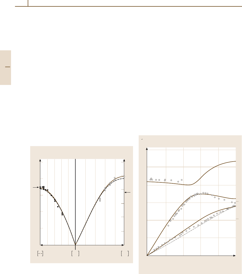
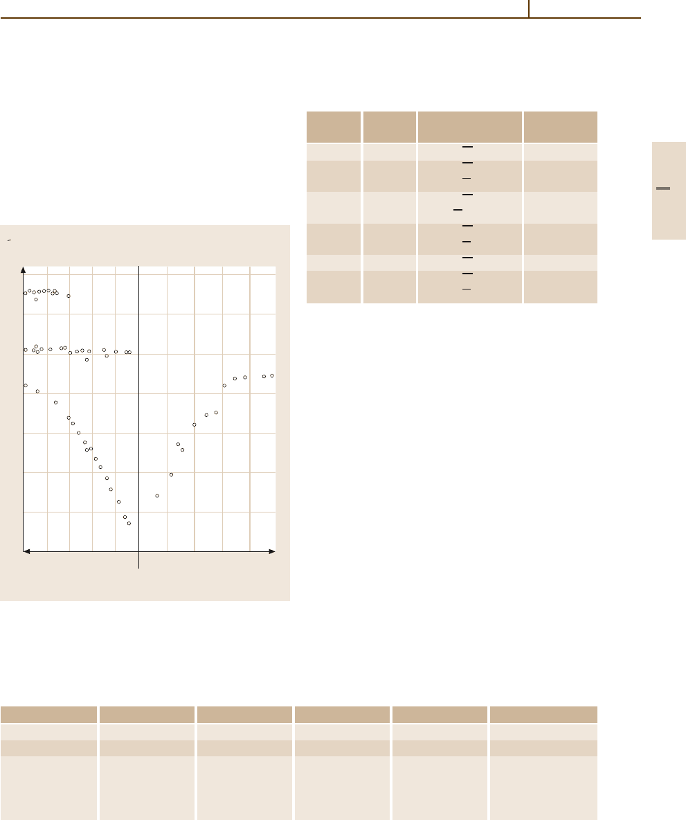
Fig. 5.2-49 Surface phonon dispersion curves for Ag(100)
measured by EELS. The filled and open circles re-
fer to different electron energies. The full and dashed
lines are theoretical fits. Energies are given in cm
−1
.
1cm
−1
= 0.1240 meV [2.80]
The experimental results have been obtained mainly
through atom and electron scattering, HATOF and
EELS.
5.2.4.1 Metals
Surface phonon bands along symmetry lines of the SBZ
are given for fcc metals in Figs. 5.2-49 – 5.2-55 and in
Table 5.2-20. In all figures the horizontal axis is the
reduced wave vector, expressed as the ratio to its value
at the zone boundary. Table 5.2-21 gives the surface
Debye temperatures for some fcc and bcc metals, as well
as the amplitudes of thermal vibrations of atoms in the
first layer: ρ
1
as compared with those of the bulk: ρ
b
.
In the harmonic approximation, the root mean square
displacement of the atoms is proportional to the inverse
of the Debye temperature.
[10]
0
1.0
18
15
12
9
6
3
0
[00]
0.2
0.4 0.6 0.8
hω (meV)
Γ
–
X
––
[ξ 0]
ξ
Ag(110)
MS
7
MS
0
S
1
Fig. 5.2-50 Surface phonon dispersion curves for Ag(110)
measured by HATOF. The solid curves are theoretical fits
[2.81]
Part 5 2.4
The Physics of Solid Surfaces 2.4 Surface Phonons 1013
Table 5.2-20 Surface phonon energies of fcc metals. References to the original articles are given in the figure captions and/or
in [2.14,15]
Metal Face Energy (meV) and mode Figure Technique
S
1
S
2
S
3
S
4
Ag
(100) 10.2 (M) 8.6 (X) Fig. 5.2-49 EELS
(110) 8.15 (X) Fig. 5.2-50 HATOF
5.0 (Y) 7.7 (Y)
(111) 8.7 (M) Fig. 5.2-51 HATOF
9.1 (K)
Al
(100) 15.1 (X) EELS
(110) 14.6 (X) Fig. 5.2-52 HATOF
8.9 (Y) 13.5 (Y)
(111) 17 (M) HATOF
18.6 (K)
Au
(110) 2 × 1 Fig. 5.2-53 EELS
(111) 7.5 (M) HATOF
7.5 (K)
Cu
(100) 16.7 (M) 20.2 (M) Fig. 5.2-54 EELS
14.1 (X) 13.6 (X)
(110)
∼
=
14 (
X) 13 (Y) HATOF
7.5 (Y)
(111) 13.3 (M) 26.1 (M) EELS, HATOF
14.0 (K)
Ni
(100) 19.2 (M) 16.1 (X) Fig. 5.2-55 EELS, HATOF
(110) 17 (X) 15.8 EELS
9.9 (Y)
(111) 17.2 (M) 32.2 (M) EELS
Pd (110) 11 (X) HATOF
6.7 (Y) 9 (Y)
Pt (111) 10.8 (M) HATOF
11.1 (K)
Table 5.2-21 Surface Debye temperatures of metals. References to the original articles are given in [2.4,6]
Crystal Bulk Θ
D
(K) Face Surface Θ
D
(K) ρ
1
/ρ
b
Technique
Ag 225
(100) 104 LEED
(110) 150–190 LEED
1.5 LEIS
1.65 MEIS
1.44 HEIS
(111) ⊥ surface 155 LEED
surface 226
247 HAS
Al 428
(100) 200 LEED
1.25 HEIS
(110) 140 LEED
(111) 200 LEED
Part 5 2.4

1014 Part 5 Special Structures
Table 5.2-21 Surface Debye temperatures of metals, cont.
Crystal Bulk Θ
D
(K) Face Surface Θ
D
(K) ρ
1
/ρ
b
Technique
Au 165
(100) 82 LEED
(110) 2 × 1 83 LEED
127 LEIS
1.55 HEIS
(111) 83 LEED
Cu 343
(100) 230 LEED
260 LEIS
1.5 MEIS
(110) 260 (150) 1.5 LEIS
1.55 MEIS
1.27 HEIS
(111) 245 LEED
Fe 467 (111) 1.18 MEIS
Ir 420
(110) 150 LEED
160 LEIS
(111) 170 LEED
Mo 450 (100) 239 LEED
Ni 450
(100) 1.46 MEIS
1.35 HEIS
(110) ⊥ surface 216 LEED
surface 344
395 MEIS
1.15 HEIS
(111) ⊥ surface 208 LEED
surface 348
1.20 HEIS
Pt 240
(100) 118 LEED
(110) 107 LEED
1.6 MEIS
(111) 111 LEED
1.3 MEIS
Rh 480 (111) 197 LEED
V 380 (100) 250 LEED
W 400
(100) 1 × 1 210 LEED
(100) c2 × 2 400 (200) LEED
1.5 HEIS
(110) 190–235 LEED
2.6, 1 HEIS
Part 5 2.4
The Physics of Solid Surfaces 2.4 Surface Phonons 1015
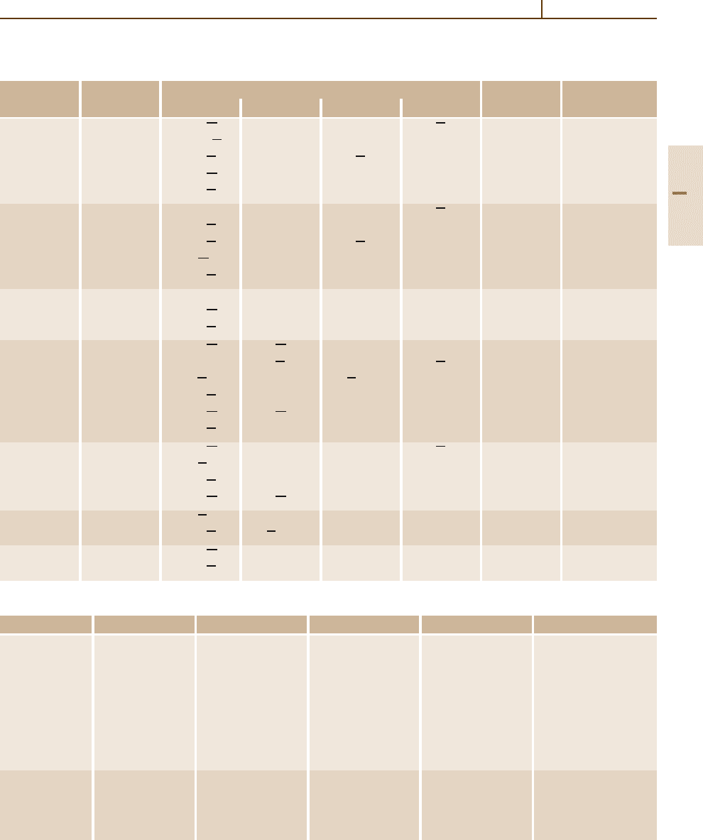
Fig. 5.2-51 Surface phonon dispersion curves for Ag(111)
measured by HATOF. Cirles are experimental points; solid
and dashed lines theoretical calculations. The hatched area
represents the projected band structure [2.82].
Very similar plots hold for Au(111) and Cu(111). For
appropriate energy parameters see Table 5.2-20
1.0
1.0
175
5.0
ν
–
(cm
–1
) ν (THz)
Y
––
X
––
150
125
100
75
50
25
0
4.5
4.0
3.5
3.0
2.5
2.0
1.5
1.0
0.5
0
[0 1]
00
[1 0][0 0]
ξξ
[0 ξ][ξ 0]
Γ
–
X
––
Γ
––
S
–
'
Y
––
'
[001] [11
-
0]
Au (110) 1 × 2
Y
––
S
–
Fig. 5.2-53 Surface phonon dispersion curves along two
directions of the SBZ for reconstructed Au(110) 2 × 1,
measured by EELS. The dashed lines are theoretical re-
sults. In the inset, the SBZ shows the folding due to the 2 ×1
reconstruction that introduces the optical bands. Energies
aregivenincm
−1
.1cm
−1
= 0.1240 meV [2.84]
00
1
1
2
ω (10
13
rad/s)
hω (meV)
24
20
16
12
8
4
0
3.5
3.0
2.5
2.0
1.5
1.0
0.5
0
001.0 0 0.5 1.0 1.0
00 10
ξξ
Γ
–
1
ξ
2
ξ
ξ
2
ξ
0
M
––
K
––
Γ
–
Ag(111)
S
1
S
1
S
1
R
1
Γ
–
[ξ 0]
hω (meV) h ω (meV)
[0 ξ]
24
20
16
12
8
4
0
0 0.2 0.4 0.6 0.8 1.0 1.0 0.8 0.6 0.4 0.2 0
24
20
16
12
8
4
0
X
––
Y
––
Γ
–
[0 0] [0 0][1 0] [0 1]
ξξ
Al (110) Al (110)
S
1
S
1
S
3
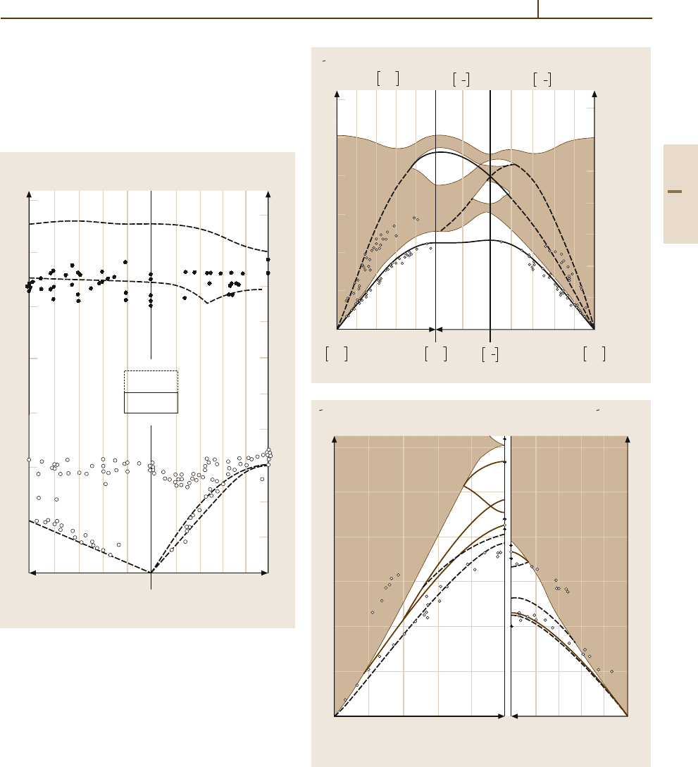
Fig. 5.2-52 Surface phonon dispersion curves for Al(110). The ex-
perimental results (circles) were obtained by HATOF. The solid and
dashed lines are theoretical fits. The shaded regions represent the
projected bulk modes [2.83]
Part 5 2.4
1016 Part 5 Special Structures
0.4
1.0
9
320
280
240
200
160
120
80
40
0
0.5 0.4 0.3 0.2 0.1 0 0 0.2 0.6 0.8
1
2
1
2
ξ
00
ξ
10
8
7
6
5
4
3
2
1
0
Γ
–
M
––
X
––
ν (THz)ν
–
(cm
–1
)
ξξ
ξ
0
Ni (001)
2
nd
2
nd
+
S
6
R
6
2
nd
2
nd
2
nd
R
s
1
st
R
3
R
4
S
4
2
nd
2
nd
2
nd
R
2
2
nd
R
1
S
2
2
nd
1
st
1
st
S
1
Fig. 5.2-55 Surface phonon dispersion curves of Ni(100) obtained
by EELS. S
j
, surface phonons; R
j
, surface resonances. Energies are
givenincm
−1
.1cm
−1
= 0.1240 meV [2.86]
0.5
1.0
140
120
100
00
80
60
40
20
0
4.0
3.5
3.0
2.5
2.0
1.5
1.0
0.5
0
1
2
1
2
00
ξξ
10
Γ
–
M
––
X
––
ν (THz)ν
–
(cm
–1
)
ξξ
ξ
0
Cu (001)
S
4
S
1
Fig. 5.2-54 Surface phonon dispersion curves for Cu(100)
measured by EELS. The solid and dashed lines
are theoretical fits. Energies are given in cm
−1
.
1cm
−1
= 0.1240 meV [2.85]
Part 5 2.4
The Physics of Solid Surfaces 2.4 Surface Phonons 1017
5.2.4.2 Semiconductors and Insulators
Phonon surface bands of some insulators and semi-
conductors are given in Figs. 5.2-56 – 5.2-58. Surface
phonon energies of alkali halide crytals are summarized
in Table 5.2-23. Since insulators and semiconductors
have in general more than one atom per unit cell, they
display both acoustical and optical branches. Surface
Debye temperatures of some semiconductors are given
in Table 5.2-22.
1.0 1.0
Γ
–
Y
––
S
–
ξ
[0 1] [1 1][0 0]
00
ξ
[0 ξ][ξξ]
14
12
10
8
6
4
2
0
hω (meV)
GaAs (110)
Fig. 5.2-56 Surface phonon dispersion curves for
GaAs(110) measured by HATOF (open circles). The en-
ergies at symmetry points are: Y, 8.3, 10.2, and 13.0meV;
Γ,10.0meV;S,8.9 meV [2.87]
Table 5.2-22 Surface Debye temperatures of semiconductors. References to the original articles are given in [2.4, 6]
Crystal Bulk Θ
D
(K) Face Surface Θ
D
(K) ρ
1
/ρ
b
Technique
GaSb 265 (110) 1.57 MEIS
InAs 249 (110) 1.65 MEIS
Si 640
(100) 430–475 HEED
1.4 HEED, LEED
(111) 2 × 1 1.45, 2.1 MEIS
300 HEIS
Table 5.2-23 Surface phonon energies of alkali halides.
References to the original articles are given in [2.14, 15]
Crystal Face Energy of mode S
1
Technique
(meV)
LiF (100) 22.9 (M) HATOF
NaF (100) 16.0 (M) HATOF
18.5 (X)
NaCl (100) 9.9 (M) HATOF
11 (X)
NaI (100) 4.1 (M) HATOF
4.9 (X)
KCl (100) 7.2 (M) HATOF
RbCl (100) 4.7 (M) HATOF
∼
=
5.7 (
X)
Part 5 2.4
1018 Part 5 Special Structures
5
4
3
2
1
0
1
2
1
2
0000
M
––
X
––
ξ
Γ
–
ξ
ξξ ξ 1–ξ ξ0
Γ
–
10
NaCl (001)
ω (10
13
rad/s)
S
7
S
1
S
6
S
3
S
4
S
2
, S
5
S
2
LM
S
8
S
1
+
Fig. 5.2-57 Surface phonon dispersion curves for NaCl(100). Theoretical projected band structure (hatched) and exper-
imental points (dots) measured by HATOF. Solid and dashed lines represent theoretical surface states and resonances.
Ordinates are given in units of 10
13
rad/s = 6.586 meV [2.88,89]
Part 5 2.4
The Physics of Solid Surfaces 2.4 Surface Phonons 1019
1.0 1.0
Γ
–
X
––
S
–
ξ
[01] [11]
[0 0]
00
ξ
[ξ 0] [ξξ]
14
12
10
8
6
4
2
0
hω (meV)
Γ
–
X
––
S
–
Si (111) 2 ×1
Γ
–
Fig. 5.2-58 Surface phonon dispersion curves for Si(111)
2× 1 measured by HATOF. Energies at symmetry points:
X, 10.2 and 11.1meV; S, 10.5 and 11.6meV. The flat
phonon mode at 10.5 meV is associated with the 2×1 recon-
struction. The surface mode couples with transverse bulk
phonons near the center of the SBZ, giving rise to consider-
able broadening. The shaded area corresponds to the width
of the 10.5 meV peak [2.90]. The energy of the optical mode
(not shown in the figure) is 56.0 meV [2.91]
5.2.4.3 Atom–Surface Potential
Many results on surface phonon dispersions are obtained
through atomic (mainly He) scattering.
The interaction of an incident atom with a surface
is described by the atom–surface potential (Fig. 5.2-59),
which consists of a hard repulsive part at short distances
and a weak van der Waals attraction at larger distances.
V (meV)
15.0
12.5
10.0
7.5
5.0
2.5
0
–2.5
–5.0
–7.5
–10.0
7
z (Å)
123456
D
h
pv
V
T
V
0
V
B
Z
m
ε
0
ε
1
B
T
Fig. 5.2-59 Typical atom–surface potential, with defini-
tions of the main interaction parameters. The surface unit
cell is shown in the inset. The numbers on the axes re-
fer to He–Ag(110) [2.92]. V
0
: surface averaged potential;
V
T
: potential at the top position; V
B
: potential at the bottom
position
The attractive contribution is often assumed in to be the
form
V
att
=−
C
3
(z −z
vW
)
3
.
In the potential well between the van der Waals potential
and the hard repulsive potential, quantized energy lev-
els ε
n
exist (see Fig. 5.2-59). Table 5.2-24 summarizes
the parameters of the atom–surface potentials for a num-
ber of surfaces and impinging atoms (or molecules).
A more extended discussion is given in [2.14,15].
Part 5 2.4
1020 Part 5 Special Structures
Table 5.2-24 Parameters of the atom–surface potential. Values of ε
n
are given in the order n = 0, 1, 2, 3 .... References
to the original papers are given in [2.15]
Crystal Face Atom/ D (meV) z
m
(Å) z
vW
(Å) C
3
(meV Å
3
) ε
n
(meV)
molecule
Ag
(110) H
2
31.7 3.27 0.755 714 25.3, 16.4, 9.7, 5.3, 2.5, 1.1
He 6.0 0.755 249 4.44, 2.18, 0.92, 0.31, 0.1
(111) H
2
32.5 2.5 0.2 714 25.5, 16.6, 9.9, 5.4, 2.5, 1.1
Al (110) He 5.2 4.47 1.71 202 3.65
Au (111) He 8.0 3.98 1.34 274 5.91
Cu (110) He 6.27 3.65 1.21 235 4.52, 2.2, 1.0, 0.3
GaAs (110) He (7) (3.5) (−0.2) (473) (4.2)
NaCl (100) He 6.1 3.49 1.03 106 4.1, 1.5, 0.31
LiF
(100) He 8.5 2.98 0.79 93 (137) 5.9, 2.46, 0.78, 0.21
Ne 13.5 192 11.7
Ni (100) He 4.2 (theory) 3.76 (theory) 218
Pd (110) He 8.05 3.60 211 6.42
Pt (110) 2×1 He 8.8 251 7.4, 5.1, 3.1, 1.5
Si (100) He 174
W (110) He 265 5.6
5.2.5 The Space Charge Layer at the Surface of a Semiconductor
Surface states in the gap of a semiconductor may trap
or loose electrons. The localized charge in surface states
is neutralized by a macroscopic space charge layer of
opposite sign, caused by accumulation or depletion of
the bulk carriers. The potential associated with the space
charge gives rise to a band bending of the bulk bands
at the surface. Band bending alters various properties
of semiconductor surfaces and is crucial for many ap-
plications, such as chemisorption, catalysis, corrosion,
and, most significantly, channel conductivity in MOS
field-effect transistors. For this reason, the problem of
the surface space charge layer is treated extensively in
the following sections.
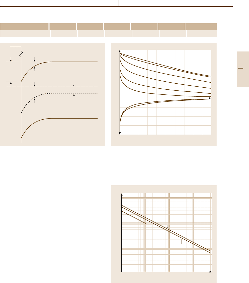
5.2.5.1 Definitions and Notation
Figure 5.2-60 shows the main parameters that character-
ize the space charge layer. With reference to the figure,
the following definitions can be given:
•
E
i
(z) is the intrinsic level: this level runs parallel to
the band edges and coincides, in the bulk, with the
intrinsic Fermi level E
ib
:
E
ib
=
E
c
+E
v
2
+
1
2
k
B
T ln
N
v
N
c
.
•
The following quantities related to band bending:
u(z) ≡
E
F
−E
i
(z)
k
B
T
,
v(z) = u(z) −u
b
≡
E
ib
−E
i
(z)
k
B
T
,
(2.1)
where v
s
, u
s
,andu
b
are the values of v(z),andu(z)
at the surface and the value of u(z) in the bulk; u
b
> 0
for n-type semiconductors and u
b
< 0 for p-type
semiconductors. If v
s
> 0 the band bends downward;
if v
s
< 0 the band bends upward. v
s
= 0 is the con-
dition for flat bands, and u
s
= 0 the condition for an
intrinsic surface.
An accumulation layer exists if v
s
and u
b
have the same
sign (as in Fig. 5.2-60).
An depletion layer exists if v
s
and u
b
have opposite signs
and u
s
and u
b
have the same sign.
An inversion layer exists if both of the pairs v
s
, u
b
and
u
s
, u
b
have opposite signs.
•
Debye length:
L
D
=
ε
0
ε
b
k
B
T
q
2
(n
b
+ p
b
)
,
(2.2)
where n
b
and p
b
are the bulk carrier concentra-
tions and q is the elementary charge. For small
Part 5 2.5
The Physics of Solid Surfaces 2.5 The Space Charge Layer at the Surface of a Semiconductor 1021
Table 5.2-25 Intrinsic Debye lengths for various semiconductors
Si Ge GaAs InP InAs InSb
Intrinsic Debye length (cm) 2.9×10
−3
7.0×10
−5
2.0×10
−1
2.7×10
−2
8.6×10
−6
2.4×10
−6
E
vac
ν
s
k
B
T
E
cs
u(z)k
B
Tu
b
k
B
T
ν(z)k
B
T
E
is
E
i
E
F
E
c
E
ν
E
νs
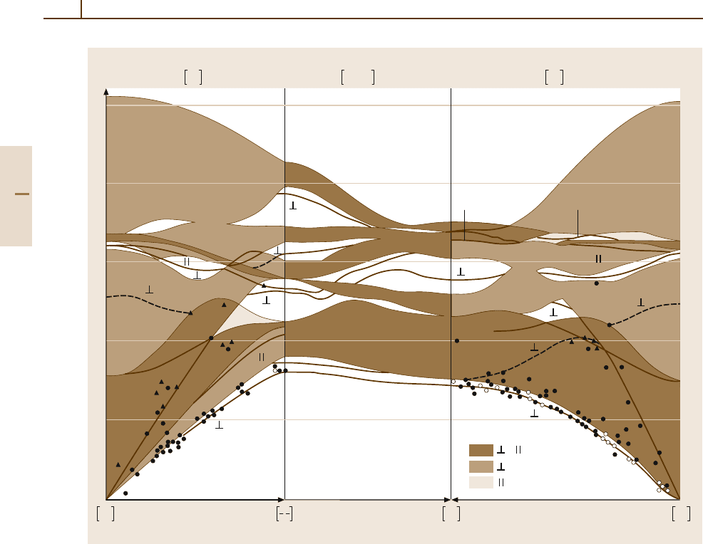
Fig. 5.2-60 Schematic behavior of the bands at the surface
of a semiconductor and definition of the main parameters.
Notice that band bending v(z) is positive when the band
bends downward
bending (< k
B
T ), the surface barrier decays as
v(z) = v
s
e
−z/L
D
. Forlargerbending, the shape of the
potential cannot be givenin analytic form, though the
thickness of thespace charge layeris still on the order
of the Debye length (see Fig. 5.2-61). Values of the
intrinsic Debye length for various semiconductors
are given in Table 5.2-25. Figures 5.2-62 and 5.2-63
give L
D
as a function of the carrier density and bulk
resistivity for various semiconductors.
•
Q
sc
is the space charge density (per unit area), Q
ss
is the charge density (per unit area) in surface states,
and
Q
total
= Q
sc
+Q
ss
; (2.3)
Q
total
=0 in the absence of an external electric field.
In the presence of an external field, Q
total
is the
charge density on the field electrode (the gate in
a MOSFET).
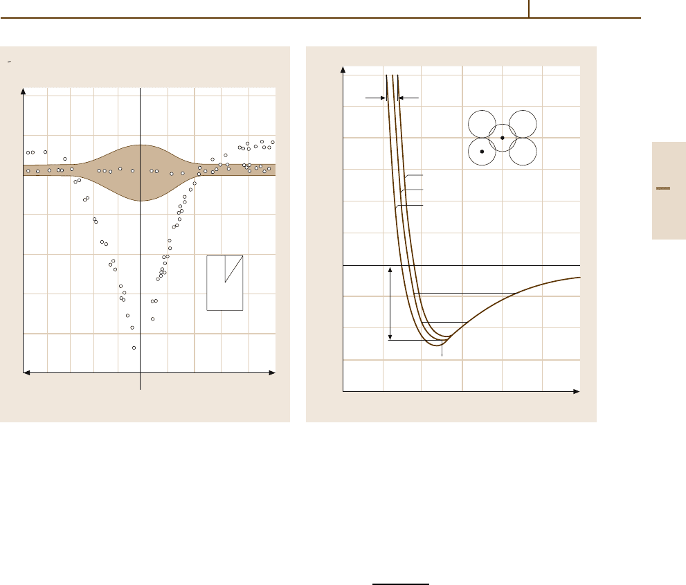
Normalized potential ⏐v⏐= (eV/ kT)
0
20
16
12
8
4
0
–4
–8
–12
–16
2.0
Normalized distance z/L
D
0.2 0.4 0.6 0.8 1.0 1.2 1.4 1.6 1.8
Accumulation
layer
Inversion and
depletion layers
⏐u
b
⏐ⱜ 10
⏐u
b
⏐=8
⏐u
b
⏐=6
⏐u
b
⏐=4
⏐u
b
⏐=2
⏐u
b
⏐ⱜ 2
u
b
= 0
u
b
=0
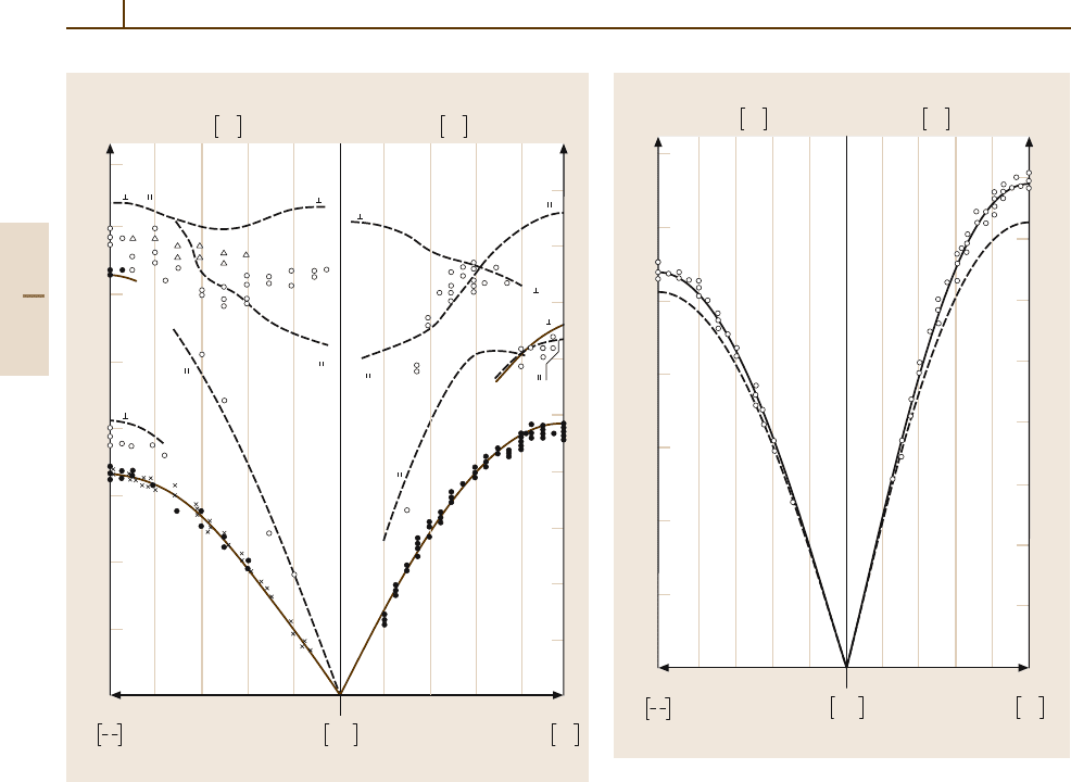
Fig. 5.2-61 Profile of the potential |v(z)| as a function of
z/L
D
plotted for |v
s
|=20 and various values of |u
b
|.The
behavior for other values of |v
s
|can be obtained by drawing
the parallel to the abscissa through the new value |v
s
| and
translating the origin of the abscissa at the value of the
interception [2.48, p. 329]
L
D
(nm)
10
3
Carrier density (cm
–3
)
10
2
10
1
10
15
10
16
10
17
10
14
Ge(ε
b
= 16.2)
Si(
ε
b
= 11.9)
p-type diamond
(
ε
b
= 5.7)
Fig. 5.2-62 Debye length as a function of carrier concen-
tration for Si, Ge and p-type diamond
Part 5 2.5