Martienssen W., Warlimont H. (Eds.). Handbook of Condensed Matter and Materials Data
Подождите немного. Документ загружается.

1002 Part 5 Special Structures
E (eV)
6
4
2
0
–2
–4
–6
–8
–10
Γ
–
M
––
Γ
–
X
––
'
X
––
Au(110)
B
D
A
C
E (eV)
7
6
5
4
3
2
1
0
–1
Γ
–
Y
––
0 0.2 0.4 0.6 0.8 1.0 1.2 1.4 1.6
k
⎮⎮
(Å
–1
)
Au(110)
1
2
3
4
E
F
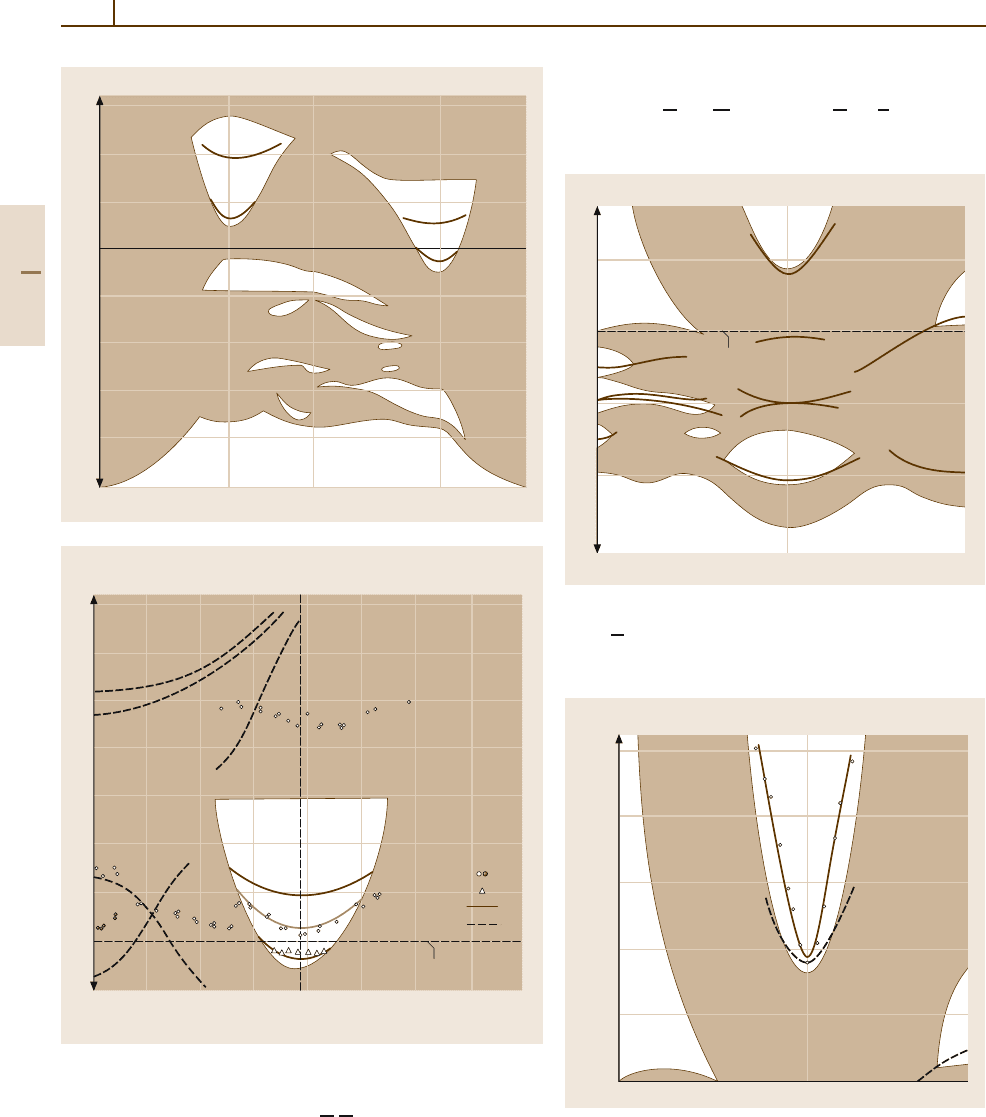
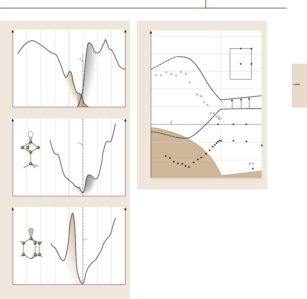
Fig. 5.2-27 Comparison of experimental results [obtained by
KRIPES for the empty states (dots) and by ARUPS for the initial
states (triangles)] with the theoretical calculations of Fig. 5.2-26.
Notice the splitting of the state near
Y(X
) probably due to the 2× 1
reconstruction [2.40,41]
Fig. 5.2-26 Theoretical projected band structure for the
unreconstructed Au(110) surface. Note that in the notation
of this figure,
X
and M correspond to YandS, respectively,
in the SBZ of Fig. 5.2-18 [2.39]
E (eV)
2
0
–2
–4
–6
Γ
–
M
––
K
––
Pd (111)
E
F
Fig. 5.2-28 Theoretical projected band structure (shaded
area) for Pd(111), showing an empty surface state
(near
Γ) and various occupied surface states and reso-
nances [2.42]
E
F
=
5
4
3
2
1
0
E (eV)
Γ
–
M
––
K
––
Pd (111)
Fig. 5.2-29 Comparison of the dispersion of the empty sur-
face state of Fig. 5.2-28 with experimental results obtained
by KRIPES [2.43]
Part 5 2.3
The Physics of Solid Surfaces 2.3 Electronic Structure of Surfaces 1003
E (eV)
0
2.0
Γ
–
M
––
Σ
––
Σ
––
– 5.0
0
– 0.5
– 1.0
– 1.5
– 2.0
– 2.5
– 3.0
– 3.5
– 4.0
– 4.5
– 5.0
0.4 0.8 1.21.2 1.6
k
⎮⎮
(Å
–1
)
E
F
SH
SHSH DD
D
W(100)
LL
1
2
3
4
ω/ω
p
0.92
0.88
0.84
0.80
0.76
0.72
0.68
0.1 0.2 0.3 0.4 0.5 0.6 0.7
q
⎮⎮
(Å
–1
)
Al(111)
RPA
RDA
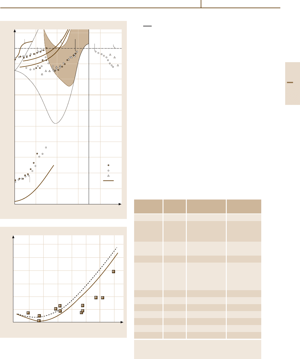
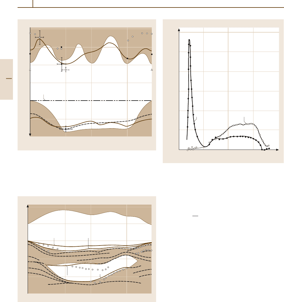
Fig. 5.2-31 Experimental dispersion of the surface plas-
mon in Al(111) as a function of q
(squares)and
comparison with theoretical results obtained with two dif-
ferent approximations [2.46]
Fig. 5.2-30 Dispersion of surface states for W(100) along
the
ΓM line obtained by ARUPS and comparison with
theory [2.44,45]
5.2.3.2 Semiconductors
The data on elemental semiconductors (including dia-
mond) are ordered according to the atomic number.
They are followed by data on some of the compound
semiconductors. For a more detailed discussion of the
various subjects, the reader may consult [2.8, 10,11] or
the books [2.47,48].
Surface Ionization Energies
The ionization energy is defined as the distance of the top
of the valence band at the surface from the vacuum level.
At low impurity concentrations, the ionization energy is
independent of doping and should, preferably, be meas-
ured in place of the work function. Table 5.2-14 reports
the ionization energies for a number of semiconductors.
Surface Core Level Shifts
In semiconductors, core levels are shifted because of
charge transfer between surface atoms. Table 5.2-15
Table 5.2-14 Ionization energies at semiconductor sur-
faces
1
Crystal Face Reconstruction Ionization
energy (eV)
Diamond (111) 2×1 6.25 (25)
Si
(100) 2×1 5.33
(111) 2×1 5.24 (9)
7×7 5.30
Ge
(111) 2×1 4.77 (2)
c(2 × 8) 4.70
GaP (110) 1×1 5.98 (3)
GaAs
(100) c(2 × 8) 5.40 (7)
c(4 × 4) 5.34 (5)
4×6 5.05
(110) 1×1 5.48 (6)
GaSb (110) 1×1 4.79 (9)
InP (110) 1×1 5.77 (8)
InAs (110) 1×1 5.37 (6)
InSb (110) 1×1 4.84 (6)
CdS (110) 1×1 6.7 (6)
CdSe (110) 1×1 6.62
CdTe (110) 1×1 5.79 (1)
1
Data are average values from various authors. Errors are
standard deviations. References to the original papers and
individual errors are given in [2.47]
Part 5 2.3

1004 Part 5 Special Structures
Table 5.2-15 Surface core level shifts for elemental semiconductors
1
Crystal Face Reconstruction Core level
Surface shifts (eV )
S
1
S
2
S
3
S
4
Diamond (111) 2×1 1s −0.8
Si
(100) 2×1
2p
−0.49 (3) −0.230 0.062 0.29 (5)
c(2 × 4) −0.485 −0.205 0.062 0.22
(111) 2×1 −0.46 (9) −0.14 0.23 (6) 0.64
7×7 −0.74 (5) −0.07 (5) 0.30 (6) 0.52 (3)
Ge
(100) 2×1
3d
−0.49 (7) −0.21 (3)
c(4 × 2) −0.60 −0.24
(111) 2×1 −0.49 (8) 0.44
c(2 × 8) −0.73 (3) −0.24 (3)
1
Data are average values from various authors. Errors are standard deviations. References to original papers and individual errors
are given in [2.47]
Table 5.2-16 Surface core level shifts at Ga and As sites in
GaAs
1
Face Reconstruction
Surface shift (eV )
Ga(3d) As(3d)
(100) c(4 × 4) +0.49 −0.285 (5)
+0.55
c(2 × 8) +0.3 −0.26 (1)
+0.55 (0)
4×6 +0.4 −0.45 (16)
−0.21
(110) 1×1 +0.28 (0) −0.373 (5)
1
Data are average values from various authors. Errors are
standard deviations. References to the original papers and
individual errors are given in [2.47]
gives the shifts for the C(1s), Si(2p), and Ge(3d) lev-
els for various faces and reconstructions. The surface
shifts of the 3d levels at the Ga and As sites of GaAs
(110) and (100) faces are given in Table 5.2-16.
The p and d levels are spin–orbit split and give rise
to doublets. Nonequivalent atoms increase further the
number of surface shifts. Up to four components are
observed in Si and Ge and up to two in GaAs.
Unresolved surface shifts for various III–V com-
pounds are given in Table 5.2-17.
Surface State Bands
The origin and nature of surface states have been dis-
cussed in the introduction to Sect. 5.2.3. Here the energy
versus k
along significant directions of the SBZ and/or
the density of states are reported for various recon-
structed/relaxed surfaces. The experimental data were
Table 5.2-17 Surface core level shifts at (110) surfaces of
III–V compounds
1
Crystal Surface shifts (eV )
Cation Anion
AlSb +0.38 −0.38
GaP +0.31 (2) −0.41 (0)
GaAs +0.28 (0) −0.370 (5)
GaSb +0.30 −0.36
InP +0.30 (2) −0.30 (1)
InAs +0.27 (1) −0.30 (0)
InSb +0.23 (1) −0.29(1)
1
Data are average values from various authors. Errors are
standard deviations. References to the original papers and
individual errors are given in [2.47]
obtained mainly with ARUPS and KRIPES or by optical,
energy loss, and STM techniques.
Because of the large amount of available data, only
a selection of dispersion curves and surfaces has been
given. For more detailed information, the reader is re-
ferred to [2.10,11].
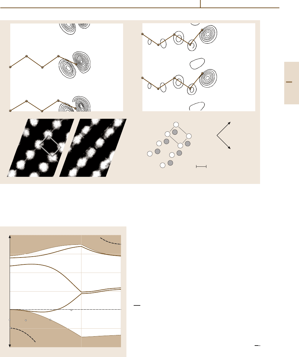
The rearrangement of unsaturated dangling bonds at
the surface is considered to be the driving force for re-
construction of semiconductors. An example of DBs is
shown in Fig. 5.2-32a,b that give contours of the charge
density for the filled (P) and empty (Ga) surface states
on the (110) surface of GaP. In Fig. 5.2-32c, a com-
parison is made with an STM image taken with a bias
voltage that allows the observation of filled and empty
states.
Figures 5.2-33 – 5.2-36 and 5.2-38 – 5.2-40 give the
E(k
) curves for selected surfaces of diamond, Si, Ge,
Part 5 2.3
The Physics of Solid Surfaces 2.3 Electronic Structure of Surfaces 1005
4Å
Ga
P
Ga
a)
b)
P
Ga
P
P
Ga
c)
[001]
[11
–
0]
d)
Fig. 5.2-32 (a) Theoretical charge density contours for the filled DB states at P sites on the relaxed GaP(110) surface,
(b) the same for the Ga site empty states, (c) comparison with constant current STM images for GaAs(110). The two STM
images refer to filled (As) states (left) and empty (Ga) states (right). The two images are obtained with positive (left)and
negative (right) bias. The rectangular unit cell is in the same (absolute) position.
(d) Schematic representation of the unit
cell. As atoms are shown as empty circles; Ga atoms as black circles [2.49,50]
E (eV)
8
6
4
2
0
–2
–4
C(111) 2 × 1
Γ
–
K
––
J
–
GaAs, and CdSe. The local density of states for Si(111)
7× 7 as obtained from ARUPS and STM spectroscopy
is shown in Fig. 5.2-37.
Transitions Between Surface States
Transitions between surface state levels give rise to
optical absorption and electron energy loss. Such tran-
sitions have been observed by SDR, RAS, ellipsometry,
and EELS. As an example, the arrows in Figs. 5.2-36
and 5.2-38 show the transitions observed in Si and
Ge(111)2 ×1. Notice the high joint density of states
caused by the quasi-parallelism of the bands along
JK.
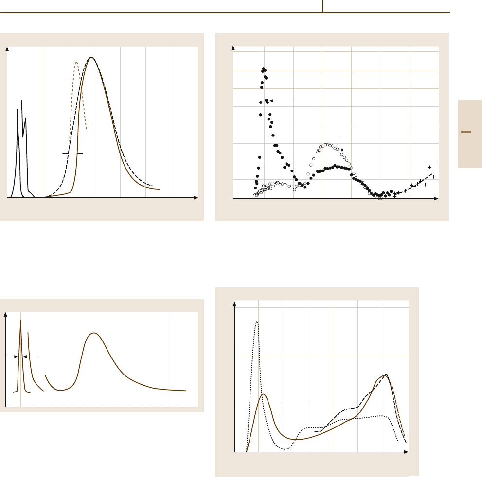
Fig. 5.2-33 Theoretical surface state bands (full lines)and
resonances (dashed lines) for a relaxed π-bonded chain
model of diamond(111)2× 1. Comparison with experimen-
tal results (open circles) obtained by ARUPS along the
ΓJ
line [2.51,52]
Part 5 2.3
1006 Part 5 Special Structures
Fig. 5.2-35 Dispersion curves of Si(100)2× 1 observed by ARUPS
at 21.2 eV. Prominent peaks are indicated by open circles, while
weak peaks and shoulders by dots. S and B peaks have surface and
bulk characters. The experimental bands should be compared with
the surface structures of Fig. 5.2-34. No optical transition clearly
associated to S
1
,S
2
(or D
down
, D
up
in Fig. 5.2-34) has been observed
in spite of the essential parallelism of the two bands (meaning a high
JDOS) [2.54,55]
E (eV)
4
2
0
–2
–4
–6
–8
–10
–12
–14
Γ
–
K
––
J
–
Γ
–
J
–
'
Si(001) 2 × 1
D
down
D
up
D
i
B
1
B
3
B
2
B
4
B
5
S
1
S
3
S'
4
S
2
S
5
Fig. 5.2-36 Surface band structure of Si(111)2 × 1. Comparison be-
tween theoretical structure based on pseudopotential calculations
for the π-bonded chain model (see Sect. 5.2.2.3, Fig. 5.2-11) and
experimental results from ARUPS. Photoemission from the excited
surface states (around the B point in the figure) is obtained by using
highly doped samples. Arrows indicate optical transitions observed
in SDR and EELS (see Figs. 5.2-41 and 5.2-43) [2.56, 57]
Γ
–
E (eV)
k
⎮⎮
J
–
'
Γ
E
F
= 0
–1
–2
–3
–4
–5
–6
–7
–8
KKW.X
Si(001) 2 ×1
S
2
S
1
S
1
B
9
S
4
B
6
B
6
B
5
B
8
B
7
B
7
B
10
W
Fig. 5.2-34 Theoretical surface band structure of Si
(100)2× 1, obtained with the asymmetric dimer model (see
Sect. 5.2.2.3, Fig. 5.2-7). D
down
and D
up
refer to the DB
bands at the down and up atoms. The bands labeled S
1
–S
5
and B
1
–B
5
are back-bond states (modified by the surface)
[2.53]
E (eV)
K
––
2.0
1.5
1.0
0.5
0
– 0.5
–1.0
–1.5
Γ
–
J
–
RS
SS
B
A
E
v
SS
RS
Γ
–
J
–
'
J
–
K
––
Si(111) 2 ×1
Part 5 2.3
The Physics of Solid Surfaces 2.3 Electronic Structure of Surfaces 1007
PE
E(eV)
–5
3
IPE
STS IPE
STS IPE
–4 –3 –2 –1 0 1 2
a)
Si(111) 7 × 7
b)
E
F
E
F
Adatoms
c)
E
F
Rest atoms
Si(111) 7 × 7
Si(111) 7 × 7
Fig. 5.2-37a–c Density of states associated with the dan-
gling bonds(on the adatoms and “restatoms”) of theSi(111)
7×7 surface (see Fig. 5.2-13), obtained
(a) by ARUPS (inte-
grated over all atoms), and
(b) and (c) by STM spectroscopy.
Notice that the gap (if present) occurs at the Fermi energy
[2.57–59]
E (eV)
K
––
Γ
–
J
–
2.5
2.0
1.5
1.0
0.5
0
– 0.5
– 1.0
– 1.5
Γ
–
E
v
J
–
'
J
–
K
––
Ge(111) 2 × 1
1
2
B
A
Fig. 5.2-38 Surface band structure of Ge(111)2 ×1. Com-
parison between theoretical structure (in the frame of
the chain model) and experimental results obtained with
KRIPES (open dots and triangles) and ARUPS (black
dots). Photoemission from excited states has been reached
by using highly doped Ge. Arrows indicate optical tran-
sitions observed in SDR and EELS (see Figs. 5.2-42
and 5.2-44) [2.60–62]
In the dielectric theory of the surface re-
sponse, the transition probability is proportional
to –Im
ˆ
ε = ε
in the optical absorption and to
Im[1/1+
ˆ
ε]=ε
/[(1+ε
)
2
+ε
2
]inEELS,
ˆ
ε = ε
−iε
being the dielectric function of the surface layer. The two
techniques give essentially the same results, as shown in
Fig. 5.2-45.
The great anisotropy of some reconstructed sur-
faces, as shown in Figs. 5.2-41 and 5.2-42, is reflected
in second-harmonic generation, which is specially
sensitive to the symmetry of the surface, being for-
bidden for centrosymmetric media (see Fig. 5.2-46 for
Si(111)2 × 1).
Surface anisotropy has given rise to the technique
of reflectance anisotropy spectroscopy (RAS), in which
linearly polarized light is modulated between two prin-
cipal directions (of the surface tensor) and the difference
Part 5 2.3
1008 Part 5 Special Structures
E (eV)
–3.2
–2.4
–1.6
– 0.8
0
0.8
1.6
Γ
–
M
––
X
––
X
––
' Γ
–
k
⎮⎮
E
v
GaAs (110)
Fig. 5.2-39 Surface band structure of GaAs(110). Comparison be-
tween theoretical structure (continous brown line) and experimental
determinations: KRIPES ( filled and open circles), ARUPS (dashed
line), and two-step photoemission (triangles). It can be noticed that
the surfacestates nearlycoincide with the band edgesof the projected
bulk band structure [2.63–67]
E (eV)
4
2
0
–2
–4
–6
Γ
–
M
––
X
––
X
––
' Γ
–
S
1
(ideal)
CdTe (110)
S
1
(relaxed)
S
2
S
3
Fig. 5.2-40 Electronic band structure of the CdTe(110) surface.
The open circles show experimental points obtained by ARUPS.
Theoretical surface states and resonances are shown by solid and
dashed lines, respectively [2.68,69]
∆R/R
×10
–2
6
5
4
3
2
1
0
123
hν (eV)
4
Si(111) 2 ×1
0
[01
-
1] [2
--
11]
Fig. 5.2-41 Surface differential reflectivity (SDR) spectra
for Si(111)2× 1, obtained with two polarizations: with the
electric vector parallel ([0
¯
11], filled circles) and perpendic-
ular ([
¯
211], open circles) to the chains of the π-bonded
chain model. For the transitions shown by arrows in
Fig. 5.2-36 (hν<1 eV) the change in reflectivity can be
observed only with the electric vector parallel to the
chains. The spectrum for hν>1 eV is associated to tran-
sitions along
ΓJ in the SBZ. The change of anisotropy
at approximately 1.2 eV is conform to the “sum rule”:
ε
x
ωdω =
ε
y
ωdω [2.70]
in the reflected light is recorded. Figure 5.2-47 gives an
example of RAS spectra for GaAs(100).
5.2.3.3 Magnetic Surfaces
The magnetic moments of atoms near the surface
plane, p
n
(n = 1 for the surface), differ from those for
the bulk, p
b
. The total incremental moment at the surface
is defined as
∆ p
sb
=
∞
n=1
( p
n
− p
b
).
Table 5.2-18 gives the values of p
b
, p
n
,and∆ p
sb
for
various ferromagnetic surfaces.
Temperature is more effective in destroying the
magnetic order at the surface than in the bulk. This
Part 5 2.3
The Physics of Solid Surfaces 2.3 Electronic Structure of Surfaces 1009
I
0
(meV)
0.2 0.4 0.4 0.8 1.0
E
loss
(arb. units)
Si(111)2 ×1
×100
× 333
20K300K
300K
Fig. 5.2-43 EELS spectra at T = 20 K and 300 K for
Si(111)2× 1 ( full and dashed lines) compared with the re-
sults of SDR of Fig. 5.2-41 (brown dashed line). The peak
of EELS is slightly displaced towards higher energies be-
cause of the energy dependence of the factor in front of the
loss function Im
1/
ˆ
ε +1
[2.70,71]
I (arb. units)
×100
×1000
580 meV
415 meV
Ge(111)2 ×1
T = 295 K
20 meV
Fig. 5.2-44 EELS spectrum of Ge(111)2 ×1 at room tem-
perature. The same considerations done in the caption of
Fig. 5.2-43 hold also here [2.73]
effect is shown in Fig. 5.2-48, where the ratio of
the polarization P at a given temperature to that
at absolute zero is plotted versus temperature. The
Curie temperature at the surface T
CS
is approxi-
mately equal to that of the bulk (T
C
) in most cases.
Table 5.2-19 reports the ratio T
CS
/T
C
for a number of
materials.
A more detailed discussion of the magnetic proper-
ties of surfaces is given in [2.13].
∆R/R (%)
Energy (eV)
0
3.5
4.0
3.5
3.0
2.5
2.0
1.5
1.0
0.5
0
0.5 1.0 1.5 2.0 2.5 3.0
along [011]
along [2
--
11]
Fig. 5.2-42 Surface differential reflectivity versus energy for
Ge(111)2 × 1 with polarization parallel and perpendicular to the
chains of the π-bonded model. The anisotropy for hν<1eV is
smaller than for Si(111)2 ×1. The same considerations done in the
caption of Fig. 5.2-41 hold also here [2.72]
ε
s
''d (Å)
Energy (eV)
0
3.5
150
Si(111) 2 ×1
100
50
0.5
0
1 1.5 2 2.5 3
Fig. 5.2-45 Comparison of SDR (dotted line) [2.70,
74], EELS (solid line) [2.75] and ellipsometry (dashed
line) [2.76] spectra for Si(111)2 ×1. The qualitative agree-
ment is remarkable [2.70,74–76]
Part 5 2.3
1010 Part 5 Special Structures
∆r/r
E (eV)
1.5
5.5
0.004
0.002
0
GaAs(001)
2.5 3.5 4.5
– 0.002
0.002
0
– 0.002
0.002
0
– 0.002
– 0.004
0.002
0
– 0.002
0.002
0
– 0.002
∆r/r
a
b
c
d
e
(2 × 4)
T = 585 °C
c(4 × 4)
189 °C
(4 × 2)
609 °C
(1 × 6)
488 °C
(4 × 6)
220 °C
Fig. 5.2-47 Reflectance anisotropy spectra for GaAs(100) grown
by MBE at different substrate temperatures in an As
4
flux of
2.8×10
−6
torr. The corresponding reconstructions (as determined
by RHEED) are also reported [2.78]
Si(111) 2 × 1
[21
-
1
-
]
[011
-
]
[21
-
1
-
]
[011
-
]
[21
-
1
-
]
[011
-
]
a)
b)
c)
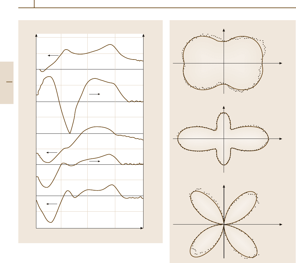
Fig. 5.2-46a–c Intensity of the secondharmonic (SH) gen-
eration signal as a function of polarization of the incidence
pump beam (1.17 eV), for Si(111)2× 1.
(a) total SH signal;
(b) SH component polarized along [2
¯
1
¯
1]; (c) SH component
polarized along [01
¯
1] [2.77]
Part 5 2.3
The Physics of Solid Surfaces 2.3 Electronic Structure of Surfaces 1011
Table 5.2-18 Surface magnetizations at given temperatures. The theoretical values are averages from various authors
(obtained with linearized-augmented-plane-wave or tight-binding methods). References to original papers are given
in [2.13]
Crystal Face T (K) Magnetic moment (Bohr magnetons) Technique
p
b
p
1
p
2
p
3
p
sb
Fe
(100) 0 2.25 2.96 2.34 2.45 1.0 Theory
(110) 0 2.22 2.60 2.37 2.28 0.66 Theory
300 2.2 2.9 (3) 0.7 (3) SPLEED
Ni
(100) 0 0.57 0.67 0.59 0.60 0.13 Theory
300 0.03 (3) SPLEED
(110) 0 0.62 0.63 0.64 0.58 0.11 Theory
(111) 0 0.58 0.63 0.64 0.58 0.11 Theory
300 0.06 (12) SPLEED
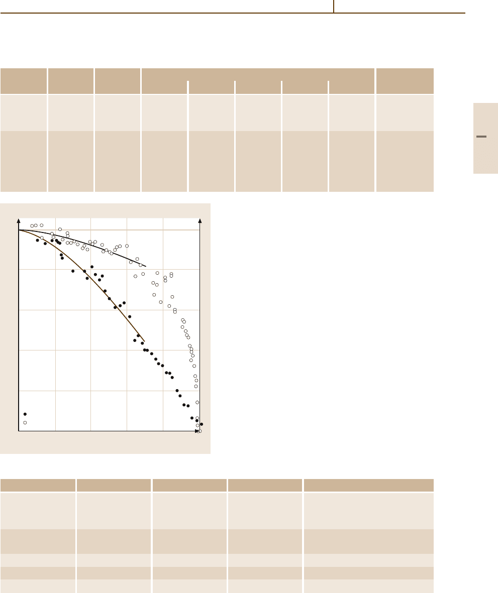
P/P
0
T/T
C
0
1.0
1.0
0.8
0.6
0.4
0.2
0
ε
0.2 0.4 0.6 0.8
Fe(110)
SPLEED
Kerr
a
b
Table 5.2-19 Surface Curie temperatures (T
CS
). References to original papers are given in [2.13]
Crystal Face T
C
(K) T
CS
/T
C
Technique
Ni
(100) 630 1 SPLEED
(110) 630 1 SPLEED
(111) 630 1 ECS
Fe
(100) 1040 1 SPARPES
(110) 1040 1 Spin-polarized secondary electrons
EuS (111) 16.71 (5) 1.000 (4) SPLEED
Gd (0001) 293 1.05–1.07 SPLEED
Tb (0001) 220 1.14 ECS
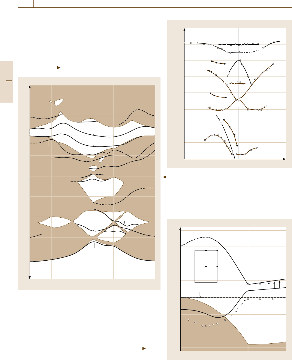
Fig. 5.2-48 Temperature dependence of magnetic order-
ing. Kerr ellipticity (representing bulk magnetization) and
normalized polarization P/P
0
of scattered electrons in
SPLEED (representing surface magnetization) as a func-
tion of T/T
C
.Thesolid curves are fits to a Bloch law:
m
1
(0) −m
1
(T ) = bT
3/2
, m
1
being the magnetization of
the first layer [2.79]
Part 5 2.3