Martienssen W., Warlimont H. (Eds.). Handbook of Condensed Matter and Materials Data
Подождите немного. Документ загружается.


1032 Part 5 Special Structures
They were named “zeolite” (“boiling stone”) in 1756 by
Cronstedt, a Swedish mineralogist, who observed their
emission of water vapor when heated. At the other size
limit, opals constitute another example of a naturally oc-
curring nanostructured material. These gems are made
up mainly of spheres of amorphous silica with sizes
ranging from 150 nm to 300 nm. In precious opals, these
spheres are of approximately equal size and can thus
be arranged in a three-dimensional periodic lattice. The
optical interferences produced by this periodic index
modulation are the origin of the characteristic iridescent
colors (opalescence).
Apart from these few examples, most nanostruc-
tured materials are synthetic. Empirical methods for the
manufacture of stained glasses have been known for
centuries. It is now well established that these methods
make use of the diffusion-controlled growth of metal
nanoparticles. The geometrical constraints on the elec-
tron motion and the electromagnetic field distribution in
noble-metal nanoparticles lead to the existence of a par-
ticular collective oscillation mode, called the plasmon
oscillation, which is responsible for the coloration of the
material. It has been noticed recently that the beautiful
tone of Maya blue, a paint often used in Mesoamer-
ica, involves simultaneously metal nanoparticles and
a superlattice organization [3.1].
The chemistry and color changes of colloidal gold
solutions were observed by Faraday during the 19th
century [3.2]. These properties were due to highly size-
dispersed gold nanoparticles.
Improvements in the diffusion-controlled growth
technique opened up the possibility of growing nano-
crystallites with better-controlled sizes and densities
and permitted its extension to various semiconduc-
tors. The fabrication of colored long-wavelength-pass
glasses and of photochromic glasses provides well-
known examples of commercial technologies based on
such methods developed decades ago. Various tech-
niques for the production and assembly of cluster- and
nanoparticle-based materials are currently under intense
study.
More recently, important technological efforts have
been made, driven by the increasing needs of the elec-
tronics industry, in order to understand and control the
growth of semiconductors at the atomic level. The de-
velopment of molecular-beam epitaxy (MBE) permitted
the control of atomic-layer-by-atomic-layer growth of
semiconductors. It has become possible to create struc-
tures made up of an alternation of different layers,
each of which is only a few atomic layers thick. The
first observation of the quantization of energy levels in
a quantum well in 1974 [3.3] opened the way to the tai-
loring of the electronic wave function in one dimension
on the nanometer scale, leading to the production of new
electronic and also magnetic materials. A new trend in
surface science is work aimed at the control of in-plane
nanostructuring, such as the formation of wire or dot
shapes, through self-organization.
In parallel to developments in the field of electron-
ics, nanostructured materials have been developed by
materials scientists and chemists also. The concept of
nanocrystalline structures emerged in the field of ma-
terials science, and polycrystals with ultrafine grain
sizes in the nanometer range have been produced. These
“nanophase materials” have been shown to have sig-
nificant modifications of their mechanical properties
compared with the coarse-grain equivalent materials.
The huge surface area of nanoporous materials has at-
tracted much attention for applications in chemistry such
as molecular sieves, catalysis, and gas sensing. This
has motivated intense research aimed at the fabrica-
tion of materials with a well-controlled composition and
nanoscale structure, such as synthetic zeolites.
The scientific and technological domains of research
on nanostructured materials cover a range of disci-
plines, from biology to physics and chemistry. However,
their convergent aspects, as well as, to some extent,
a common type of approach, have been recognized re-
cently in the realm of nanoscience and nanotechnology,
under the term “nanostructured materials”, or simply
“nanomaterials”.
For an extended review on nanotechnology see the
recently published Handbook of Nanotechnology [3.4].
5.3.1.2 Definitions
In their broadest definition, nanostructured materials
show structural features with sizes in the range from
1 nm to a few hundred nanometers in at least one dimen-
sion. This very general criterion actually includes very
diverse physical situations.
First, as is apparent from the previous section, each
nanostructured material is associated with a specific
novel property or a significant improvement in a spe-
cific property resulting from the nanoscale structuring.
As a consequence, the type of nanostructuring used
must be based on a spatial dependence of some param-
eter related to the property under consideration. This
parameter could be, for example, the material density,
transport parameters, or the dielectric constant. Another
consequence is that the upper size limit of the structural
features varies depending on the property considered,
Part 5 3.1
Mesoscopic and Nanostructured Materials 3.1 Introduction and Survey 1033
from a molecular size for molecular-sieve properties up
to the wavelength of light for the optical properties.
Second, in addition to the nanometer-scale struc-
turing, a larger-scale ordering of the unit patterns
may be necessary for the existence of the property
sought. For example, the particular optical prop-
erties of opals mentioned above require the silica
nanospheres to show a long-range order with a co-
herence length well beyond a micron. The same
considerations hold for quantum-well superlattices, for
example. In other cases, the nanosized building blocks
do not need long-range order to provide a specific
property, but still require some degree of short-range
organization. For example, an electrical conductiv-
ity appears only above a critical percolation density
of conducting particles. Finally, some properties of
nanostructured materials simply reflect a correspond-
ing intrinsic property of their individual building blocks.
This is the case, for instance, in nanoparticles embed-
ded in glass or polymer matrices for optical-filtering
applications.
Two main technological approaches may be defined:
•
The top-down manufacturing paradigm consists in
downscaling the patterning of materials to nano-
meter sizes. This allows the generation of materials
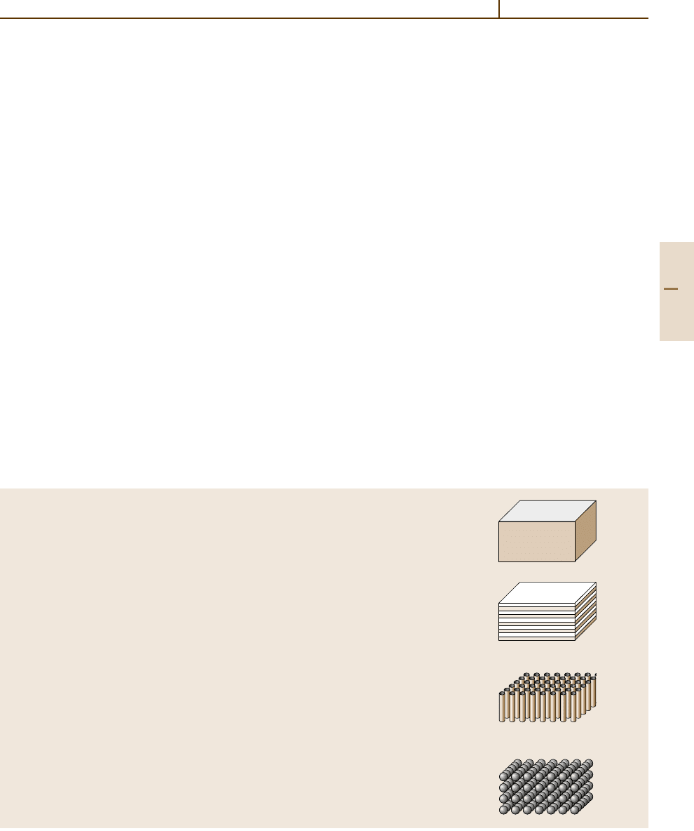
Table 5.3-1 Examples of reduced-dimensional material geometries, and definitions of their dimensionality and of the associated
type of confinement
L
X,Y,Z
> L
0
No nanostructures No confinement Bulk material
L
X,Y
> L
0
> L
Z
Two-dimensional (2-D) One-dimensional (1-D) Wells
nanostructures confinement
L
X
> L
0
> L
Y,Z
One-dimensional (1-D) Two-dimensional (2-D) Wires
nanostructures confinement
L
0
> L
X,Y,Z
Zero-dimensional (0-D) Three-dimensional (3-D) Dots
nanostructures confinement
which are coherently and continuously ordered from
macroscopic down to nanoscopic sizes.
•
The bottom-up paradigm is based on the atomically
precise fabrication of entities of increasing size. It
is the domain of macromolecular and supramolecu-
lar chemistry (dendrimers, engineered DNA, etc.)
and of cluster and surface physics (epitaxy, self-
assembly, etc.).
Mesoscopic materials form the subset of nanostruc-
tured materials for which the nanoscopic scale is large
compared with the elementary constituents of the mater-
ial, i. e. atoms, molecules, or the crystal lattice. For the
specific property under consideration, these materials
can be described in terms of continuous, homogeneous
media on scales less than that of the nanostructure. The
term “mesoscopic” is often reserved for electronic trans-
port phenomena in systems structured on scales below
the phase-coherence length Λ
Φ
of the carriers.
Most of the common nanomaterials can be classified
in terms of dimensionality, according to the number of
orthogonal directions X, Y, Z in which the structural pat-
terns referred to above have dimensions L
X,Y,Z
smaller
than the nanoscopic limit L
0
. This leads to the classical
definitions of dimensionality summarized in Table 5.3-1.
However, it should be noted that experimental situations
Part 5 3.1
1034 Part 5 Special Structures
can be encountered in which the dimensionality may
not be so obviously defined. For instance, the structural
patterns may be formed by nonrectilinear wires which
occupy a surface or a volume or may be branched.
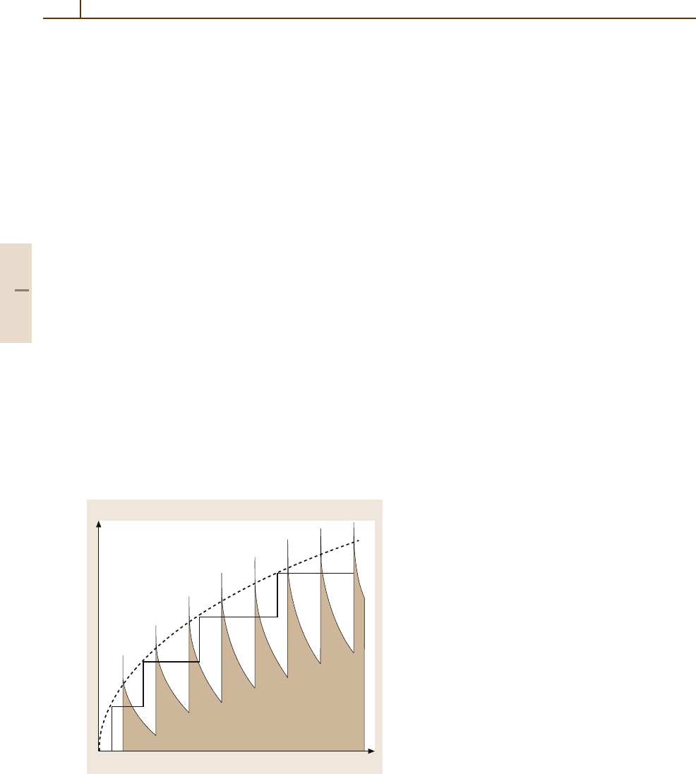
The structure of the density of states (DOS) in nano-
structures is strongly dependent on the dimensionality.
A free 3-D motion yields a band characterized by three
wave vectors k
x
, k
y
, k
z
. The corresponding DOS de-
pends smoothly on the energy E,as(E − E
0
)
1/2
, where
E
0
is the energy of the bottom of the band. Confine-
ment into a 2-D system splits the band into subbands,
and leaves only two continuously varying wave vectors
k
x
, k
y
in each subband. The DOS for each subband is
then constant above the energy E
0
N
of its bottom state.
The overall DOS is discontinuous, with a stepwise struc-
ture that is characteristic of quantum wells (Fig. 5.3-1).
Confinement in one additional dimension splits each 2-D
subband further into a set of 1-D subbands. Each 1-D
subband is characterized by only one continuously vary-
ing wave vector k
x
, and two quantum numbers N, M.
The DOS corresponding to the subband N, M has a vari-
ation of the form (E −E
0
N,M
)
−1/2
, with a divergence at
the bottom of the subband E
0
N,M
. The DOS of a quan-
tum wire thus has a more pronounced structure than
does a 2-D well, with a larger number of subbands,
each one starting as a peak (Fig. 5.3-1). Finally, con-
finement in all three dimensions creates a completely
discrete, atom-like set of states. The DOS of a quan-
DOS
E
Fig. 5.3-1 Schematic illustration of the density of states for
3-D motion of a free electron (dashed line), a 2-D quantum
well (solid line), and a 1-D quantum wire (shaded area )as
a function of energy
tum dot thus consists of a series of δ-functions (not
represented in Fig. 5.3-1). The sharpening of the DOS
at specific energies induced by quantum confinement is
the origin of many improvements in the properties of
nanostructured materials compared with bulk materials.
This spectral concentration enhances all resonant effects
and increases the energy selectivity. The preservation of
these effects when one is dealing with an ensemble of
quantum-confined systems requires a high homogeneity.
5.3.1.3 Specific Properties
The specific properties of nanostructured materials can
have two different possible origins:
•
Size effects, which result from the spatial confine-
ment of a physical entity inside an element of the
nanoscale structural pattern. Such an element is
called a low-dimensional system. An example is the
confinement of electron wave functions inside a re-
gion whose size is smaller than the electron mean
free path. This class of effects may give birth to
completely new properties.
•
Boundary effects, which are a consequence of the
significant volume fraction of matter located near
surfaces, interfaces, or domain walls. Processes that
take place only at such locations may be highly
favored, and properties specific to structural bound-
aries may also be greatly enhanced.
For a recent comprehensive review of the basic prin-
ciples of the origin of the properties of nanostructured
materials, see [3.5].
5.3.1.4 Organization of this Chapter
Many classification schemes for nanostructured ma-
terials exist. These may be based on their chemical
composition, on the technique for their manufacture,
or on their dimensionality. These schemes, however, are
often suitable only for a subset of materials. Moreover,
they generally address only one particular scientific or
technological approach and its associated community
of specialists. Since, as noted above, most nanostruc-
tured materials are associated with a specific property,
we have chosen a presentation based on properties. This
scheme allows us to include all nanostructured materials
and is accessible to the largest possible readership.
Consistently with the materials approach of this
chapter and with its limited size, only the proper-
ties of statistical ensembles of nanostructures will be
considered. The specific behaviors of individual nano-
Part 5 3.1
Mesoscopic and Nanostructured Materials 3.2 Electronic Structure and Spectroscopy 1035
sized objects or devices are not included. Since surface
and interface properties are treated in another section,
emphasis will be put here on size effects. Properties
related to electronic confinement and its consequences
for spectral properties are addressed in Sect. 5.3.2. Ef-
fects of the confinement of electromagnetic fields are
treated in Sect. 5.3.3. Magnetic size effects are addressed
in Sect. 5.3.4. Finally, we list and briefly describe in
Sect. 5.3.5 some generic methods for preparation of
nanostructured materials.
5.3.2 Electronic Structure and Spectroscopy
5.3.2.1 Electronic Quantum Size Effects
Confined electronic systems are quantum systems in
which carriers, either electron or holes, are free to move
only in a restricted number of dimensions. In the con-
fined dimension, the sizes of the structural elements
are of the order of a few de Broglie wavelengths of
the carriers or less. Depending on their dimensionality,
these structures can be quantum dots (0-D), quantum
wires (1-D), or quantum wells (2-D). Quantum wells
are typically produced by the alternate epitaxial growth
of two or moredifferent semiconductors. Quantum wires
are less commonly encountered, since their fabrication
procedures are much more complicated (Sect. 5.3.4).
One of the most dramatic effects, called the quan-
tum size effect, consists in a redistribution of the energy
spectrum of the system, the density of states becom-
ing discrete along the confinement direction. In the
most simple “particle in a box” model of a quan-
tum well, the energies of the corresponding eigenstates
are
E
N,k
x
,k
y
= N
2
π
2 2
2md
2
+
k
2
x
+k
2
y
2
2m
,
(3.1)
where m is the effective mass of the carrier, d is the
confinement dimension, and N is a quantum number.
The first term appears because of the quantized motion
in the z direction, whereas the second term represents
the energy of the free x, y motion, characterized by
wave vectors k
x
, k
y
. Each value of N defines a semi-
infinite subband of energy levels. Although the “particle
in a box” model is simplistic compared with real sys-
tems, this limiting case is often successful in describing
the essential features of quantum size effects [3.6].
The importance of the quantum size effect is mainly
determined by the energy differences E
N+1
− E
N
.
Quantum size effects become observable when this sep-
aration exceeds the thermal energy of the carriers, so
that adjacent subbands are differently populated. Since
the energy difference E
N+1
− E
N
increases with N,
it could be anticipated that quantization effects would
be more important for processes involving higher sub-
bands. However, the practical observation of such effects
in systems with a large Fermi energy (E
F
E
1
), i. e.
in metals, is often made difficult because of con-
tributions from many levels and the appearance of
collective phenomena such as plasmon oscillations,
which wash out quantization effects. Most of the spec-
tral data revealing quantum well states in metal films
a few monolayers thick have been obtained by angle-
resolved photoemission for Cs on Cu(111) [3.7] and for
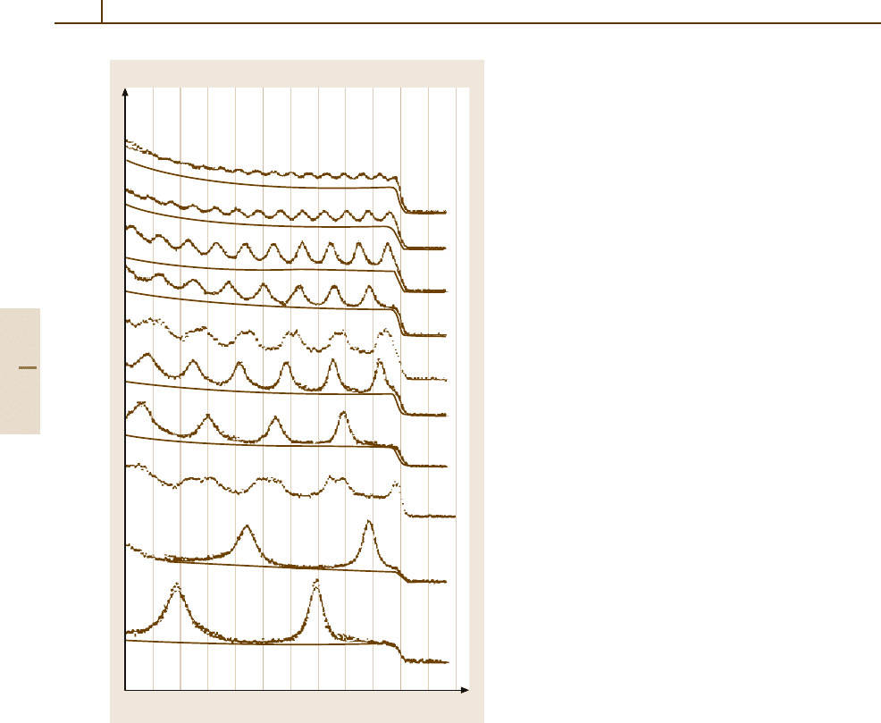
Ag on Au(111) [3.8]. The Fabry–Perot-like regularly-
spaced spectrum of energy levels appears particularly
clearly in a study of Ag films on Fe(100) for thick-
nesses up to more than 100 monolayers (Fig. 5.3-2).
The superposition at half-integer coverages (27.5and
42.5 monolayers) of two sets of peaks corresponding
to the two closest integer thicknesses emphasizes the
extreme sensitivity to surface homogeneity. Quanti-
tatively, the characteristic roughness of well barriers
must be much below the de Broglie wavelength of
the quantum states observed. This is another reason
why quantum size effects have been observed mainly
in semiconductor nanostructures, which have large
Fermi wavelengths, rather than in metals, which have
Fermi wavelengths comparable to a few crystal lattice
periods.
The existence of discrete electronic states of elec-
trons confined in a small metal cluster has been observed
to influence the thermodynamic stability of the system,
in particular during the production of sodium clus-
ters in supersonic beams composed of the metal vapor
and an inert gas. The statistics of the relative abun-
dances of different particle sizes reveal the existence
of “magic numbers” for the number of atoms in the
cluster, N = 8, 20, 40, 58, 92,... [3.9]. This has been
interpreted in terms of the existence of degenerate en-
ergy levels in a spherical well with infinite-potential
walls. Particularly stable structures are obtained when
the number of valence electrons is such that it leads
to a closed-shell electronic structure, i. e. a structure
with a completely filled energy level and an empty up-
Part 5 3.2
1036 Part 5 Special Structures
2
119
95
71
57
42.5
42
28
27.5
14
12
10
Photoemission intensity (arb. units)
Binding energy (eV)
= 16 eV
ν
h
Ag / Fe (100)
Thickness
(ML)
Fig. 5.3-2 Dots: experimental normal photoemission spec-
tra for Ag quantum wells deposited on Fe(100), with various
thicknesses. Solid curves: fits and background functions.
(After [3.12])
per level. The electronic shell structure induces similar
size dependences in the work function and the electron
density, through Friedel-like oscillations [3.10]. The se-
ries of “magic numbers” is discernible up to N = 1430.
For larger particles, the relative abundance of different
sizes is controlled instead by the stability and relative
sizes of the various facets of the surface of the par-
ticle. It is noteworthy that 2-D quantum well states are
also predicted to produce oscillatory variations of the
energetics of a film as a function of thickness, with
similar “magic numbers” for the number of deposited
monolayers [3.11].
5.3.2.2 Breakdown of the Momentum
Conservation Rule
As a result of the Heisenberg uncertainty principle, lo-
calization of carriers in a confinement volume spreads
their wave functions in reciprocal space. The possible
overlap in k space of electron and hole wave functions
breaks the rule of conservation of crystal momentum.
In other words, the momentum needed for a transi-
tion at a different k may be provided by scattering
from the boundaries. This consequence of quantum
confinement is particularly meaningful for nanostruc-
tures based on indirect-band-gap semiconductors, for
which luminescence from recombination of the lowest-
energy electrons and holes is forbidden in the bulk
material, but becomes increasingly possible for sys-
tems of decreasing size, with a scaling law of d
−6
for dots [3.13]. The observation of bright luminescence
from nanoporous silicon samples [3.14] was, from the
start, interpreted in terms of quantum confinement into
silicon nanowires [3.14,15]. This observation triggered
an important researchactivity motivated by theindustrial
prospect of being able to incorporate silicon photonic
elements into the current silicon technology. Although
it has been shown that other phenomena such as sur-
face effects and phonon modes (discussed later) come
into the play, and that more complicated geometries
including both quantum dots and quantum wires have
to be considered, the role of quantum confinement in
the luminescence of porous silicon is generally con-
sidered to be central, at least for the “red” part of the
luminescence. The studies of nanostructure-induced lu-
minescence have been extended to porous GaP [3.16,17]
and SiC [3.18], two other semiconductors with an indi-
rect band gap, and the results parallel those for porous
silicon. Quantum-confined luminescence has been ob-
served in indirect-gap semiconductor nanostructures
with well-controlled geometries such as silicon and
germanium 2-D wells [3.19] and quantum dots (see
e.g. [3.20]), which may possibly be integrated into light-
emitting devices [3.21]. The observation of optical gain
in silicon nanocrystals [3.22] opens up new prospects
for the creation of silicon-based lasers [3.23].
5.3.2.3 Excitons
in Quantum-Confined Systems
A very general effect of quantum confinement in semi-
conductors is a widening of their optical band gap. For
the model system of an infinite-barrier 2-D quantum
well, (3.1) shows that the lowest energy(N =1) of a con-
Part 5 3.2
Mesoscopic and Nanostructured Materials 3.2 Electronic Structure and Spectroscopy 1037
duction electron is increased compared with the bottom
of the conduction band. A similar consideration applies
to the lowest energy of a hole in the valence band. Both
effects contribute to an increase in the minimum ex-
citation energy of the system compared with the bulk
band gap. This blueshift has a comparable magnitude in
2-D and 0-D structures [3.24]. This constitutes the lead-
ing contribution to the characteristic blueshifts in the
optical spectra of strongly quantum-confined semicon-
ductor systems. However, the confinement of oppositely
charged carriers at reduced separations also has dramatic
effects on the electron–hole Coulomb energy and thus
on exciton formation.
Two regimes of exciton confinement must be distin-
guished, depending on the confinement size d compared
with the Bohr radius a
∗
0
of the Mott–Wannier exciton in
the bulk semiconductor [3.25]. The weak-confinement
regime corresponds to sizes such that d ≥ 4a
∗
0
.Inthis
regime, therelative electron–holemotion, and in particu-
lar its binding energy, is essentially left unchanged. The
exciton can still be considered as a quasiparticle, but its
center-of-mass translational motion becomes quantized.
A simple model [3.26] of a single-point quasiparticle
with mass M
Ex
equal to the total mass of the exciton,
M
Ex
= m
∗
e
+m
∗
h
, explains the observed frequency shifts.
The translational state with the lowest energy, N = 1,
which is the only optically allowed state, has a nonzero
kinetic energy. Compared with an infinite-sized system,
the lowest excitation energy in the weak-confinement
regime is thus increased by
∆E
Weak
=
π
2 2
2M
Ex
d
2
. (3.2)
Like that for electron states, this shift has comparable
magnitudes for various dimentionalities. In the weak-
confinement regime, the exciton wave function still
involves combinations of several conduction-band elec-
tron states and valence-band hole states, and not only the
lowest-energy states. The quantization of carrier states
does not change significantly the average energy of all
of the states involved in exciton formation. As a con-
Table 5.3-2 1s exciton Bohr radius for various semiconductors
Direct-band-gap semiconductors
Semiconductor CuCl Diamond CdTe CdS GaN CdSe GaAs
a
∗
B
(nm) 0.7 0.85 2.8 2.9 3.6 5.6 12
Indirect-band-gap semiconductors
Semiconductor GaP SiC Si Ge
a
∗
B
(nm) 1.17 2.7 4.9 17.7
sequence, in the weak-confinement regime, the exciton
energy is not affected by the band gap increase which
results from the increase in the energy levels of the
lowest electron and hole states discussed above. The
weak-confinement model is very suitable for describing
spectral variations in nanoparticles of semiconductors
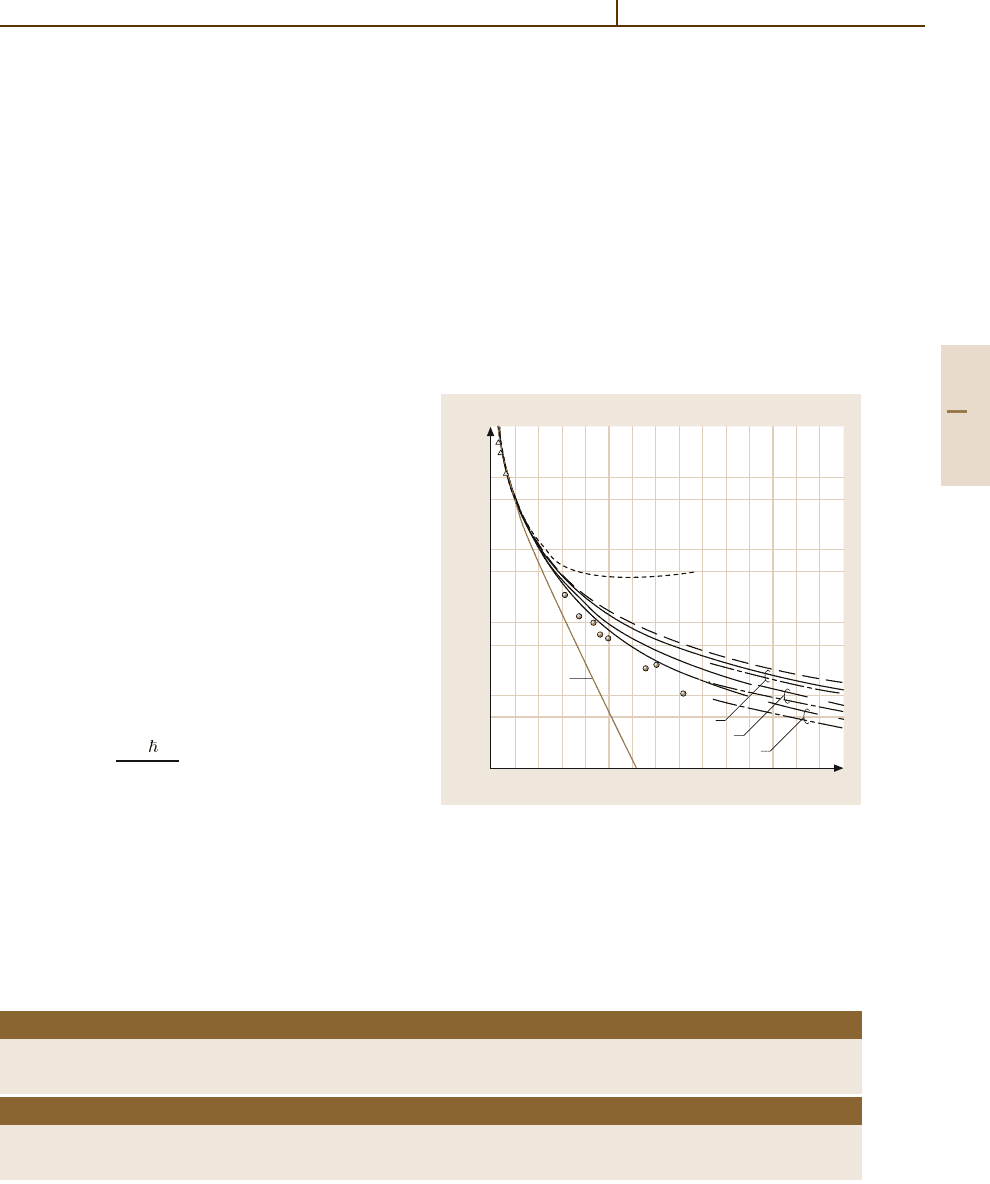
with low exciton Bohr radii, such as CuCl (Table 5.3-2),
as shown in Fig.5.3-3.
The strong-confinement regime corresponds to the
opposite limit, d ≤2a
∗
0
. In that case the relativeelectron–
hole motion is strongly affected by the barriers. In the
direction of restricted motion, the kinetic energies of the
lowest-energy electron and hole states determined by
the quantum confinement are larger than the Coulomb
0.005
0.01
0.05
0.1
0.5
1.0
5
10
R/a*
B
02468101214
Energy shift (E*
Ry
)
σ
= ∞
σ
= 1
σ
= 5
σ
= 10
Fig. 5.3-3 Observed values of energy shifts in the lu-
minescence peak of CuCl nanocrystals in NaCl (circles)
and in the absorption peak of CdS nanocrystals in sili-
cate glass (triangles), compared with theoretical models:
weak-confinement model (dashed-dotted lines), strong
confinement model (short-dashed line); σ =m
∗
h
/m
∗
e
is con-
sidered as a fixed parameter. (After [3.25])
Part 5 3.2
1038 Part 5 Special Structures
attraction. The exciton states are thus formed from un-
correlated electron and hole states of the “particle in
a box” model in the confinement direction, whereas spa-
tially correlated electron–hole bound states can still be
formed in the unrestricted directions. This yields 2-D,
1-D, and 0-D excitons in quantum wells, quantum wires,
and quantum dots, respectively. The binding energy of
a 2-D exciton can be deduced from the two-dimensional
hydrogen atom problem [3.27]. The exciton Rydberg
series changes from E
∗
3-D
=−R
∗
/n
2
in the 3-D case
to E
∗
3-D
=−R
∗
/(n −1/2)
2
in the 2-D case, where R
∗
is the Rydberg constant for the exciton. This effect is op-
posed by the increased energy required for the creation
of an electron–hole pair owing to the confinement of the
carrier motion. The variation of the excitation energy of
the first 1s-like exciton state in the regime of strong 1-D
confinement is then
∆E
2-D
Strong
=
π
2 2
2µd
2
−3R
∗
, (3.3)
where µ is the electron–hole reduced mass, such that
µ
−1
= m
∗
e
−1
+m
∗
h
−1
. The first term is larger than the
term due to the weak confinement of exciton motion
(3.2) because of the difference between µ and M
Ex
.The
0-D case is treated in detail in [3.25]. The variation of
the minimum excitation energy in the regime of strong
3-D confinement is
∆E
0-D
Strong
=
π
2 2
2µd
2
−1.786
e
2
4πεd
−0.248R
∗
. (3.4)
The divergence as d
−1
of the second term for small sizes
results from the increased Coulomb interaction in this re-
stricted geometry compared with the 2-D case. As could
be expected, the case of a 1-D exciton in a quantum wire
is intermediate between 0-D and 2-D, with a divergent
Coulomb interaction which is sublinear in d
−1
[3.28].
For all dimensionalities, in the strong-confinement
regime, the increased kinetic energy of quantum-
confined carriers is dominant, and a blueshift of the
optical gap is observed that varies continuously between
the weak- and the strong-confinement regimes. How-
ever, the considerably increased exciton binding energy
in strongly confinedsystems yields more pronounced ex-
citon effects. For the most widely used semiconductors,
excitonic effects are not discernible in room tempera-
ture spectra without quantum-confinement. However,
in strongly confined geometries of any dimensionality,
many semiconductors exhibit well-resolved excitonic
peaks since the exciton binding energy can then ex-
ceed the thermal excitation energy k
B
T . Both the
blueshift of the spectra and the increasingly pronounced
excitonic absorption are very evident in II–VI semi-
conductor nanoparticles, as exemplified in Fig. 5.3-4
for CdSe [3.29]. Semiconductor-doped glasses, formed
from a dispersion of II–VI semiconductor crystallites
in a silicate glass matrix, are the basis for some com-
mercially available yellow-to-red long-wavelength-pass
optical filters [3.30]. The glasses with a cutoff wave-
length in thevisible contain CdS
1−x
Se
x
nanocrystallites,
and the glasses used in the infrared filters contain es-
sentially CdTe nanocrystallites. Their abrupt absorption
band edge can be tuned by adjusting the composition,
the size [3.31], and, as will be discussed later, the
concentration of the particles. In other widely used semi-
conductors, such as Si, Ge, and III–V compounds, the
valence bands may have complex features and contain
light- and heavy-hole branches. The two corresponding
types of excitons will have different characteristics, such
as different binding energies.
The second important consequence of the squeez-
ing of excitons in the strong-confinement regime is
an increase in the optical matrix element associated
with their excitation. A detailed discussion of this ef-
fect can be found in [3.32]. Its origin is the stronger
overlap of electron and hole wave functions in reduced-
dimensional excitons. This effect, associated with the
concentration of oscillator strength into a few discrete
transitions, has found many applications in optoelec-
tronic devices. Certainly the most important is the
fabrication of electrically powered multiple-quantum-
well (MQW) lasers in In
x
Ga
1−x
As and Al
x
Ga
1−x
As
(infrared), and Al
x
Ga
y
In
1−x−y
P (red). These systems
are widely used today in data storage systems, bar code
scanners, laser pointers, and printers. The physics and
technology of MQW lasers are far beyond the scope
of this section. Details may be found in [3.33], for ex-
ample. 1-D and 0-D systems are also of interests for laser
systems [3.34]. Laser applications of quantum-confined
systems exploit the enhanced stimulated-emission coef-
ficients that result from the increased transition matrix
elements and spectral sharpening in quantum-confined
systems. Besides MBE-grown devices, optical gain in
chemically synthesized CdSe nanocrystal quantum dots
has been achieved [3.35]. The operation of an op-
tically pumped solid-state distributed-feedback (DFB)
laser based on a CdSe-doped titania matrix gain medium
has been demonstrated [3.36]. The output color of this
laser can be selected by choosing appropriately sized
nanocrystals and tuning the DFBperiod accordingly (see
Fig. 5.3-5).
Another consequence ofthe large oscillatorstrengths
associated with confined-exciton transitions is the
Part 5 3.2
Mesoscopic and Nanostructured Materials 3.2 Electronic Structure and Spectroscopy 1039
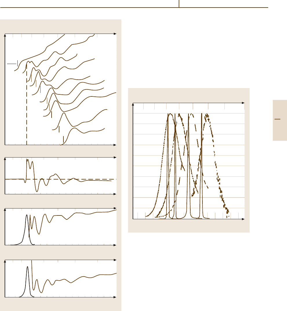
700 600 500 400
a)
115
67
51
46
38
32
30
28
26
19
b)
c)
d)
1.8 2.0 2.2 2.4 2.6 2.8 3.0 3.2
1.8 2.0 2.2 2.4 2.6 2.8 3.0 3.2
1.8 2.0 2.2 2.4 2.6 2.8 3.0 3.2
1.8 2.0 2.2 2.4 2.6 2.8 3.0 3.2
Wavelength (nm)
D (Å)
OD
–∆
67Å
Intensity
67Å
PL
PLE
Intensity
10 K
10 K
10 K
10 K
62Å
PL
PLE
Energy (eV)
Energy (eV)
Energy (eV)
Energy (eV)
Absorbance (arbitrary units)
enhancement of nonlinear optical and electrooptical co-
efficients. Nonlinear absorption and electroabsorption
correspond to changes in absorption coefficients in-
duced by high-intensity optical fields and large DC
Fig. 5.3-4 (a) Low-temperature (10 K) absorption spectra
of CdSe dots dispersed in a polymer matrix, for vari-
ous mean diameters.
(b) Nanosecond saturated-absorption
spectra for 67 Å dots. The pump beam had a 7 ns FWHM.
The excitation photon energy, 1.984 eV, is prolonged as
a dashed vertical line from
(a) for easier comparison.
The horizontal dashed line corresponds to ∆OD = 0.
(c),(d) Photoluminescence(PL) and photoluminescence-
excitation(PLE, observed at 2.022 eV) spectra for 67 Å
dots
(c) and for 62 Å dots (d). (After [3.29])
1.8 1.9 2.0 2.1 2.2 2.3 2.4
700 650 600 550 500
Energy (eV)
Wavelength (nm)
a
b
cd
Fig. 5.3-5 The photoluminescence emission spectra of
CdSe nanocrystals with different radii (dashed and dotted
lines, for radii of 2.7nm,2.4nm,and2.1nm)andof1.7nm
CdSe/ZnS core–shell nanocrystals (the radii are given in
order of increasing photon energy) at low pump power, and
at a pump power above the laser threshold (solid lines).
The nanocrystals were dispersed in a titania film used in
a distributed-feedback laser configuration at 80 K. (After
[3.36])
electric fields, respectively. Exciton–exciton interactions
increase the energy of doubly excited states in quantum
dots, which results in large saturable absorption effects
(see Fig. 5.3-4b). The absorption saturation intensities
may be as low as those of saturable dye solutions,
but these systems have an increased robustness and
the possibility of including them in solid-state media.
Part 5 3.2
1040 Part 5 Special Structures
PbS-nanocrystal-doped glasses with an absorption satu-
ration intensity of 0.2MW/cm have been realized [3.37]
and used as intracavity passive Q-switches in picosec-
ond [3.37] and femtosecond [3.38] pulsed near-infrared
lasers. The Frantz–Keldysh effect is also strongly en-
hanced in quantum-confined systems [3.39]. Moreover,
the well-resolved excitonic transition shows quantum-
confined Stark effects (QCSEs) with particularly large
magnitudes. In quantum wells, this effect usually con-
sists of a redshift of the absorption and a strong decrease
of its oscillator strength, and has been exploited for the
realization of fast, low-drive-voltage electrooptic mod-
ulators [3.40], which could possibly be integrated with
semiconductor lasers [3.41].
5.3.2.4 Vibrational Modes
and Electron–Phonon Coupling
The description in terms of phonons of the vibrational
properties of solids assumes a translational invariance.
It can be used only inside domains of homogeneous
mechanical properties with sizes larger than the spa-
tial extension of the phonon considered, typically given
by its wavelength λ
ph
. Similarly to the case of vi-
brational modes of impurities in crystals [3.43], the
confinement of phonons in structures smaller than λ
ph
leads to the localization and the quantization of the
vibrational modes. For typical solids, the phonon fre-
quencies affected by confinement sizes on the 1–100 nm
scale have frequencies on the order of 0.1–10 THz, i. e.
thermal phonon energies and higher, and both acous-
tic and optical phonons are affected. The frequencies of
the quantized modes, as well as their damping rates,
depend on the size, shape, and nature of the envi-
ronment of the nanostructure and its interfaces. The
electron–phonon coupling may be strongly modified
by phonon confinement, with manifestations in the
transport properties and in the optical absorption and
luminescence.
In 2-D systems, two-dimensional phonons appear,
with properties and consequences similar to those of
surface phonons. The role of in-plane propagating
phonons in electron–phonon scattering rates has been
demonstrated in metal films [3.44] and in Si/Ge quan-
tum wells [3.45]. Phonon propagation perpendicular to
a quantum-well superlattice produces Bragg-like selec-
tive transmission [3.46]. The formation of phonon band
gaps results from the zone folding of the LA and TA
phonons propagating perpendicular to the layers, and
is well described by a mesoscopic model of a periodic
series of homogeneous layers [3.47].
When we move to 0-D systems, the phonon spec-
trum changes to a set of size-dependent discrete lines.
As in the case of 2-D systems, most data on the var-
ious vibrational modes of metal nanoparticles [3.48]
and semiconductor nanocrystals (see e.g. [3.49] and
references therein) embedded in solid matrices have
been obtained by spontaneous-Raman-scattering spec-
troscopy. The lowest frequencies are well described
by the simple Lamb theory [3.50] of the vibration of
a homogeneous, elastic sphere. The breathing mode,
the mode of lowest energy, is usually the best resolved
one. A detailed calculation of the mesoscopic acoustic
modes in quantum dots of various compositions em-
bedded in various matrices can be found in [3.51]. The
availability of ultrafast pulsed lasers, with a pulse du-
ration shorter than the period of an acoustic vibration
mode, offers the possibility to monitor the vibrations
in the time domain rather than the frequency domain, as
shown in Fig. 5.3-6 for 3 nm PbS quantum dots in a poly-
mer matrix. Similar experiments have been performed
on Ag particles of various sizes in a glass matrix [3.52].
These experiments offer a unique opportunity to ana-
lyze the damping of these vibrations, which is generally
attributed to radiation of acoustic waves into the matrix.
The modes excited by ultrafast laser pulses are
usually not the same as those detected by spontaneous-
Raman spectroscopy, mainly for symmetry reasons
[3.53] (see Fig. 5.3-7). Moreover, the symmetry se-
lection rules depend on the mechanism of excitation
by the laser pulse. A thermal mechanism provokes
0.04
0.035
0.03
0.025
0.02
0.015
0.01
0.005
0
012345
∆T/T
Delay (ps)
Fig. 5.3-6 Time-domain breathing-mode acoustic oscilla-
tions in 3 nm PbS quantum dots embedded in a polymer
matrix, observed by transient saturated absorption. (After
[3.42])
Part 5 3.2
Mesoscopic and Nanostructured Materials 3.2 Electronic Structure and Spectroscopy 1041
2
1
0
54 3 2 1
S
01
S
21
0 0.5 1
S
01
'
Frequency (THz)
1/radius (nm
–1
)
S
01
S
21
R (nm)
Fig. 5.3-7 Frequency of the coherent-phonon and Raman
peaks as function of PbSe dot size. The solid lines repre-
sent the calculation on the assumption that the stress at the
dot boundary is zero, and the dashed line represents the cal-
culation with a rigid boundary condition. The matrix was
a phosphate glass. The inset represents the displacement
in the S
01
and S
21
spheroidal modes. The coherent-phonon
and Raman frequencies are assigned to the S
01
and S
21
modes, respectively. (After [3.53])
breathing-mode (S
01
) oscillations, whereas electrostric-
tive excitation excites the elongation mode (S
12
).
Figure 5.3-7 also illustrates the parallel dependences
of the modes excited by Raman scattering and by ultra-
fast laser-pulse on particle size. These dependences are
consistent with a Lamb model with boundary conditions
corresponding to the absence of stress.
The confinement also influences the electron–
phonon coupling. For example, in GaAs, each quantized
optical-phonon mode produces a Huang–Rhys ladder in
the phonon sidebands in the spectrum of the exciton
transition [3.55]. A scaling law in d
−3
is predicted for
the effective coupling strength [3.55]. It has been shown
that the luminescence spectra of silicon nanocrystals
exhibit not only a no-phonon peak but also TO- and
TA-phonon-assisted peaks. Hence, besides the break-
down of the momentum conservation rule discussed
above, an increased electron–phonon interaction also
favors luminescence in this indirect-band-gap semicon-
ductor. This coupling prevails for moderate confinement
energies, below 0.7 eV [3.56]. The enhanced electron–
phonon coupling results not from phonon quantization
but rather from an increased overlap factor [3.57].
In metal particles, the main consequence of changes
in the electron–phonon couplings is a variation of the
electron relaxation rates. This effect depends strongly
on the intensity regime of the excitation, but exper-
iments carried out at weak excitation on Ag and Au
nanoparticles in various matrices show a strong increase
of the relaxation rate, i. e. a decrease of the electron–
lattice energy exchange time, with quantum confinement
(see Fig. 5.3-8) [3.54]. In this case also, the increased
0.9
0.8
0.7
0.6
0.5
1.2
1.0
0.8
0.6
0.4
0 5 10 15 20 25 30
0 5 10 15 20 25 30
τ (ps)
a)
Ag
τ (ps)
b)
Au
Nanoparticle diameter (nm)
Nanoparticle diameter (nm)
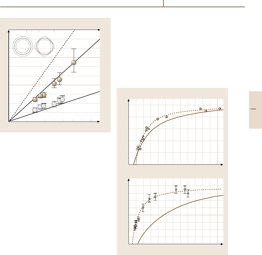
Fig. 5.3-8 (a) Size dependence of the measured electron-
lattice energy exchange time τ
e–ph
for silver clusters in
BaO
−
P
2
O
5
(circles), in Al
2
O
3
(open squares), in MgF
2
(diamond), in a polymer (up triangles), and deposited on
a glass substrate (down triangle). The solid line is the result
of the theoretical model proposed by the authors of [3.54].
The dashed line is a guide to the eye.
(b) As (a), for gold
clusters in Al
2
O
3
(squares), in colloidal solutions prepared
using a radiolysis technique (triangles), and in commer-
cially available colloidal solutions (circles). (After [3.54])
Part 5 3.2