Справочник по мощным TMOS транзисторам (MOTOROLA)
Подождите немного. Документ загружается.

4–298
Motorola TMOS Power MOSFET Transistor Device Data
LEAD DEFINITIONS
Symbol Lead Description
V
DD
Logic Supply
HIN Logic Input for High Side Gate Driver Output (HO), In Phase
SD Logic Input for Shutdown
LIN Logic Input for Low Side Gate Driver Output (LO), In Phase
V
SS
Logic Ground
V
B
High Side Floating Supply
HO High Side Gate Drive Output
V
S
High Side Floating Supply Return
V
CC
Low Side Supply
LO Low Side Gate Drive Output
COM Low Side Return
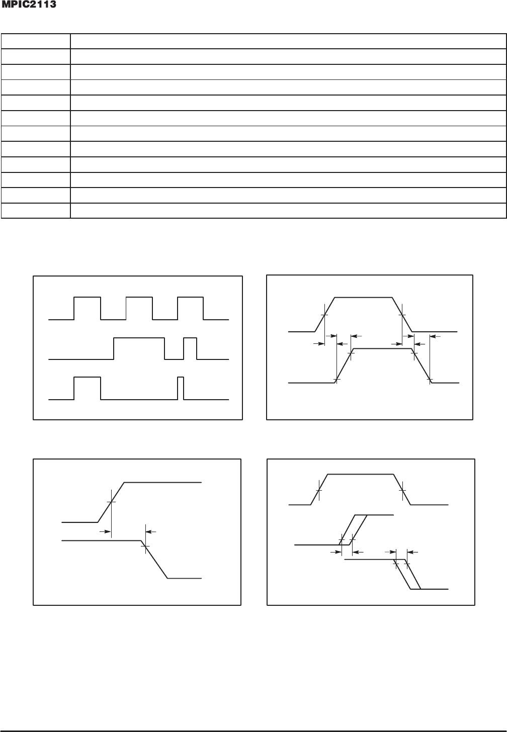
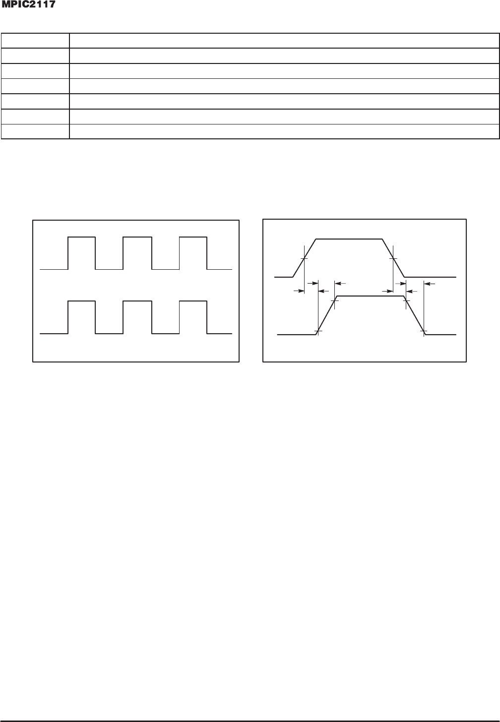
Figure 1. Input / Output Timing Diagram
Figure 2. Switching Time Waveform
Definitions
Figure 3. Shutdown Waveform Definitions
HIN
LIN
SD
HO
LO
HIN
LIN
HO
LO
10% 10%
90% 90%
t
on
t
r
50% 50%
t
off
t
f
Figure 4. Delay Matching Waveform
Definitions
50%
90%
HO
LO
SD
t
sd
10%
50%50%
90%
HIN
LIN
LO HO
LO HO
MT MT
4–299
Motorola TMOS Power MOSFET Transistor Device Data
Power Products Division
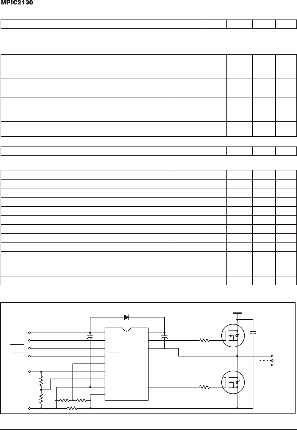
The MPIC2117 is a high voltage, high speed, power MOSFET and IGBT driver.
Proprietary HVIC and latch immune CMOS technologies enable ruggedized mono-
lithic construction. The logic input is compatible with standard CMOS outputs. The
output drivers feature a high pulse current buffer stage designed for minimum driv-
er cross–conduction. The floating channel can be used to drive an N–channel pow-
er MOSFET or IGBT in the high side or low side configuration which operates from
10 to 600 volts.
• Floating Channel Designed for Bootstrap Operation
• Fully Operational to +600 V
• Tolerant to Negative Transient Voltage
• dV/dt Immune
• Gate Drive Supply Range from 10 to 20 V
• Undervoltage Lockout
• CMOS Schmitt–triggered Input with Pull–down
• Output In Phase with Input
PRODUCT SUMMARY
V
OFFSET 600
V
MAX
I
O+/– 200
mA/420
mA
V
OUT 10
–
20
V
t
on/off
(typical)
125
&
105
ns
V
B
8V
CC
IN
COM
HO
V
S
7
6
5
1
2
3
4
V
B
8V
CC
IN
COM
HO
V
S
7
6
5
1
2
3
4
8 LEADS DIP
MPIC2117P
8 LEAD SOIC
MPIC2117D
PIN CONNECTIONS
(TOP VIEW)
This document contains information on a new product. Specifications and information herein are subject
to change without notice.
REV 1
SEMICONDUCTOR TECHNICAL DATA
Device
Package
SINGLE CHANNEL DRIVER
ORDERING INFORMATION
MPIC2117P PDIP
D SUFFIX
PLASTIC PACKAGE
CASE 751–05
(SO–8)
8
1
P SUFFIX
PLASTIC PACKAGE
CASE 626–05
8
1
MPIC2117D SOIC
4–300
Motorola TMOS Power MOSFET Transistor Device Data
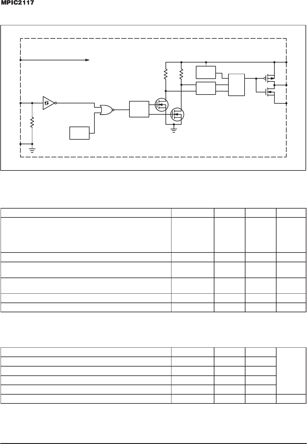
SIMPLIFIED BLOCK DIAGRAM
PULSE
GEN
UV
DETECT
PULSE
FILTER
HV
LEVEL
SHIFT
V
S
V
B
HO
R
R
S
Q
V
CC
IN
COM
UV
DETECT
ABSOLUTE MAXIMUM RATINGS
Absolute Maximum Ratings indicate sustained limits beyond which damage to the device may occur. All voltage parameters are absolute
voltages referenced to COM. The Thermal Resistance and Power Dissipation ratings are measured under board mounted and still air
conditions.
Rating
Symbol Min Max Unit
High Side Floating Supply Absolute Voltage V
B
–0.3 625 V
DC
ggy g
High Side Floating Supply Offset Voltage
B
V
S
V
B
–25 V
B
+0.3
DC
High Side Floating Output Voltage
LiS lVlt
V
HO
V
V
S
–0.3
03
V
B
+0.3
25
Logic Supply Voltage
Logic In
p
ut Voltage
V
CC
V
IN
–0.3
03
25
V
CC
+0 3
L
og
i
c
I
npu
t
V
o
lt
age
V
IN
–
0
.
3
V
CC
+
0
.
3
Allowable Offset Supply Voltage Transient dV
S
/dt – 50 V/ns
*Package Power Dissipation @ T
A
≤ +25°C (8 Lead DIP)
(8 Lead SOIC)
P
D
–
–
–
1.0
0.625
Watt
Thermal Resistance, Junction to Ambient (8 Lead DIP)
(8 Lead SOIC)
R
θJA
–
–
125
200
°C/W
Operating and Storage Temperature T
j
, T
stg
–55 150 °C
Lead Temperature for Soldering Purposes, 10 seconds T
L
– 260 °C
RECOMMENDED OPERATING CONDITIONS
The Input/Output logic timing Diagram is shown in Figure 1. For proper operation the device should be used within the recommended condi-
tions. The V
S
offset rating is tested with all supplies biased at 15 V differential.
High Side Floating Supply Absolute Voltage
V
B
V
S
+10 V
S
+20
V
High Side Floating Supply Offset Voltage V
S
Note 1 600
High Side Floating Output Voltage V
HO
V
S
V
B
Logic Supply Voltage V
CC
10 20
Logic Input Voltage V
IN
0 V
CC
Ambient Temperature T
A
–40 125 °C
Note 1: Logic operational for V
S
of –5 to +600 V. Logic state held for V
S
of –5 V to –V
BS
.
4–301
Motorola TMOS Power MOSFET Transistor Device Data
ELECTRICAL CHARACTERISTICS (T
A
= 25°C unless otherwise specified)
Characteristic Symbol Min Typ Max Unit
STATIC ELECTRICAL CHARACTERISTICS
V
BIAS
(V
CC
, V
BS
) = 15 V unless otherwise specified. The V
IN
, V
TH
and I
IN
parameters are referenced to COM. The VO and IO parameters
are referenced to COM and are applicable to the respective output leads: HO or LO.
Logic “1” Input Voltage @ V
CC
= 10 V V
IH
6.4 – –
V
DC
Logic “1” Input Voltage @ V
CC
= 15 V V
IH
9.5 – –
Logic “1” Input Voltage @ V
CC
= 20 V V
IH
12.6 – –
Logic “0” Input Voltage @ V
CC
= 10 V V
IL
– – 3.8
Logic “0” Input Voltage @ V
CC
= 15 V V
IL
– – 6.0
Logic “0” Input Voltage @ V
CC
= 20 V V
IL
– – 8.3
High Level Output Voltage, V
BS
–V
O
@ V
IN
= V
IH
, I
O
= 0 A V
OH
– – 100
mV
Low Level Output Voltage, V
O
@ V
IN
= V
IL
, I
O
= 0 A V
OL
– – 100
Offset Supply Leakage Current @ V
B
= V
S
= 600 V I
LK
– – 50
µA
Quiescent V
BS
Supply Current @ V
IN
= 0 V or V
CC
I
QBS
– 50 –
Quiescent V
CC
Supply Current @ V
IN
= 0 V or V
CC
I
QCC
– 70 –
Logic “1” Input Bias Current @ V
IN
= 15 V I
IN+
– 20 40
Logic “0” Input Bias Current @ V
IN
= 0 V I
IN–
– – 1.0
V
BS
Supply Undervoltage Positive Going Threshold V
BSUV+
– 8.5 –
V
V
BS
Supply Undervoltage Negative Going Threshold V
BSUV–
– 8.2 –
V
CC
Supply Undervoltage Positive Going Threshold V
CCUV+
– 8.6 –
V
CC
Supply Undervoltage Negative Going Threshold V
CCUV–
– 8.2 –
Output High Short Circuit Pulsed Current
@ V
OUT
= 0 V, V
IN
= 15 V, PW ≤ 10 µs
I
O+
200 250 –
mA
Output Low Short Circuit Pulsed Current
@ V
OUT
= 15 V, V
IN
= 0 V, PW ≤ 10 µs
I
O–
420 500 –
DYNAMIC ELECTRICAL CHARACTERISTICS
V
BIAS
(V
CC
, V
BS
) = 15 V unless otherwise specified
Turn–On Propagation Delay @ V
S
= 0 V t
on
– 125 –
ns
Turn–Off Propagation Delay @ V
S
= 600 V t
off
– 105 –
Turn–On Rise Time @ C
L
= 1000 pF t
r
– 80 –
Turn–Off Fall Time @ C
L
= 1000 pF t
f
– 40 –
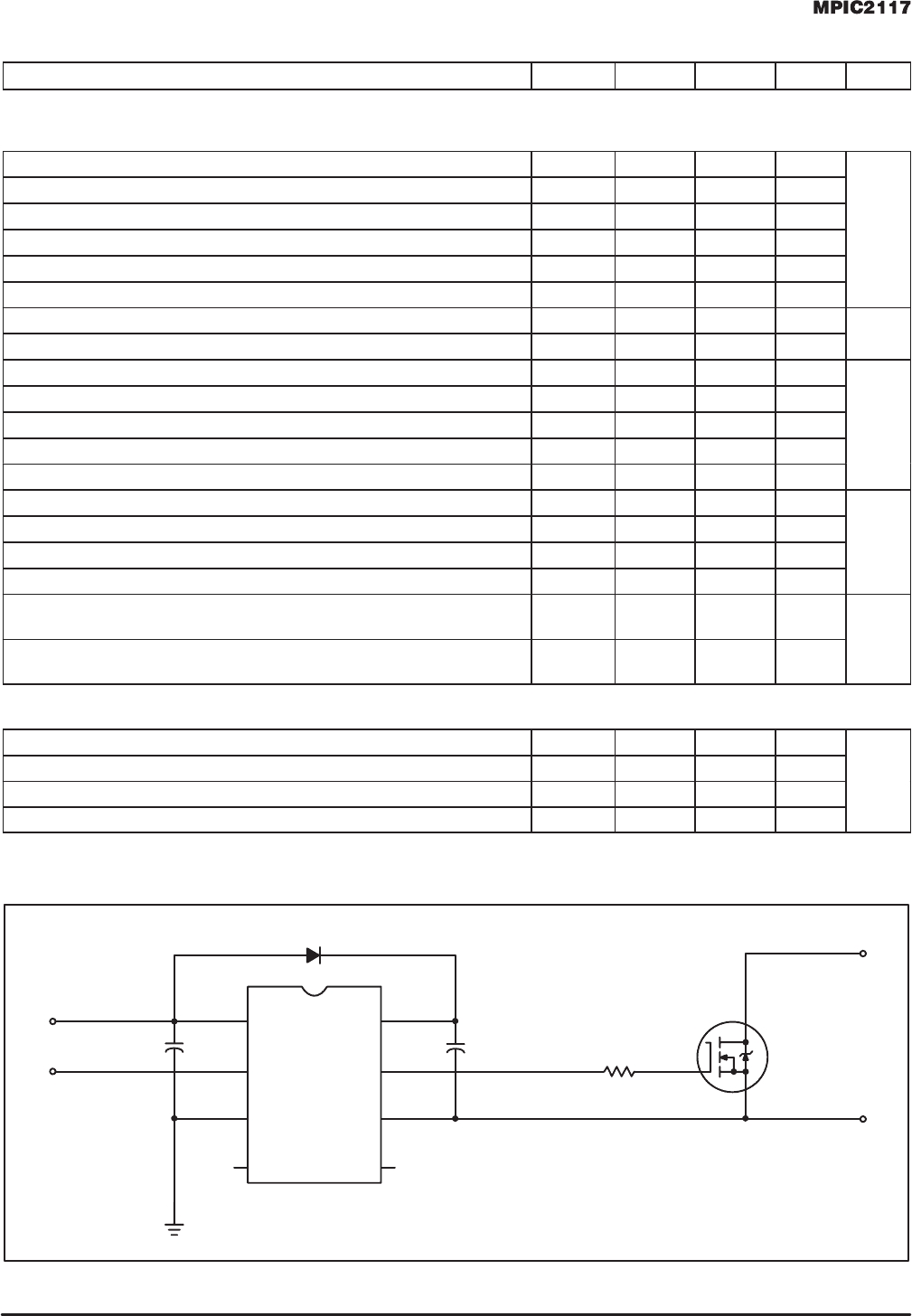
TYPICAL CONNECTION
IN
V
CC
V
CC
IN
COM
V
S
HO
V
B
4–302
Motorola TMOS Power MOSFET Transistor Device Data
LEAD DEFINITIONS
Symbol Lead Description
V
CC
Logic Supply
IN Logic Input for High Side Gate Driver Outputs (HO), In Phase with HO
COM Logic Ground
V
B
High Side Floating Supply
HO High Side Gate Drive Output
V
S
High Side Floating Supply Return
Figure 1. Input / Output Timing Diagram
Figure 2. Switching Time Waveform
Definitions
HO
IN
HO
IN
10% 10%
90% 90%
t
on
t
r
t
off
t
f
50% 50%
4–303
Motorola TMOS Power MOSFET Transistor Device Data
Power Products Division
The MPIC2130 is a high voltage, high speed, power MOSFET and IGBT driver
with three independent high side and low side referenced output channels for
3–Phase applications. Proprietary HVIC technology enables ruggedized monolith-
ic construction. Logic inputs are compatible with 5 V CMOS or LSTTL outputs. A
ground referenced operational amplifier provides an analog feedback of bridge
current via an external current sense resistor. A current trip function which termi-
nates all six outputs is also derived from this resistor. An open drain FAULT signal
is provided to indicate that an over–current or undervoltage shutdown has oc-
curred. The output drivers feature a high pulse current buffer stage designed for
minimum driver cross–conduction. Propagation delays are matched to simplify use
in high frequency applications.
The floating channels can be used to drive N–channel power MOSFET or
IGBT’s in the high side configuration which operate from 10 to 600 volts.
• Floating Channel Designed for Bootstrap Operation
• Fully Operational to +600 V
• Tolerant to Negative Transient Voltage
• dV/dt Immune
• Gate Drive Supply Range from 10 to 20 V
• Undervoltage Lockout for All Channels
• Over–current Shut Down Turns Off All Six Drivers
• Independent Half–bridge Drivers
• Matched Propagation Delay for All Channels
• Outputs Out of Phase with Inputs
PRODUCT SUMMARY
V
OFFSET 600
V
MAX
I
O+/– 200
mA/420
mA
V
OUT 10
–
20
V
t
on/off
(typical)
675
&
425
ns
Deadtime (typical)
2.5
s
This document contains information on a new product. Specifications and information herein are subject
to change without notice.
REV 1
SEMICONDUCTOR TECHNICAL DATA
Device
Package
3–PHASE
BRIDGE DRIVER
ORDERING INFORMATION
(TOP VIEW)
PIN CONNECTIONS
P SUFFIX
PLASTIC PACKAGE
CASE 710–02
MPIC2130P PDIP
28
1
1
2
3
4
5
6
7
8
22
23
24
25
26
27
28
9
21
20
10
11
12
13
14
17
18
19
16
15
V
CC
HIN1
HIN2
HIN3
LIN1
LIN2
LIN3
FAULT
ITRIP
CAO
CA–
V
SS
V
SO
LO3
V
B1
HO1
V
S1
V
B2
HO2
V
S2
V
B3
HO3
V
S3
LO1
LO2
4–304
Motorola TMOS Power MOSFET Transistor Device Data
SIMPLIFIED BLOCK DIAGRAM
LATCH
UV
DETECTOR
DRIVER
PULSE
GENERATOR
LEVEL
SHIFTER
SET
RESET
LATCH
UV
DETECTOR
DRIVER
PULSE
GENERATOR
LEVEL
SHIFTER
SET
RESET
LATCH
UV
DETECTOR
DRIVER
SET
RESET
DRIVER
DRIVER
DRIVER
CLEAR
LOGIC
PULSE
GENERATOR
LEVEL
SHIFTER
INPUT
SIGNAL
GENERATOR
INPUT
SIGNAL
GENERATOR
INPUT
SIGNAL
GENERATOR
UNDER–
VOLTAGE
DETECTOR
FAULT
LOGIC
CS
V
S3
V
B3
V
S2
V
S1
V
B1
HO1
H1
L1
H2
L2
H3
L3
–+
CURRENT
AMP
0.5 V
CURRENT
COMPARATOR
V
B2
HO2
HO3
LO1
LO2
LO3
V
SO
HIN1
HIN2
HIN3
LIN1
LIN2
LIN3
FAULT
V
CC
V
SS
ITRIP
CAO
CA–
ABSOLUTE MAXIMUM RATINGS
Absolute Maximum Ratings indicate sustained limits beyond which damage to the device may occur. All voltage parameters are absolute
voltages referenced to V
SS
. The Thermal Resistance and Power Dissipation ratings are measured under board mounted and still air condi-
tions.
Rating
Symbol Min Max Unit
High Side Floating Absolute Voltage
High Side Floating Su
pp
ly Offset Voltage
V
B1,2,3
V
S123
–0.3
V
B123
–25
625
V
B123
+0 3
V
DC
High
Side
Floating
Su ly
Offset
Voltage
High Side Floating Output Voltage
Fi d S l V lt
V
S1
,
2
,
3
V
HO1,2,3
V
V
B1
,
2
,
3
–
25
V
S1,2,3
–0.3
03
V
B1
,
2
,
3
+0
.
3
V
B1,2,3
+0.3
25
Fixed Supply Voltage
Low Side Driver Return
V
CC
V
SO
–0.3
V
CC
–0.3
25
V
CC
+0.3
Low Side Output Voltage
L
og
i
c
Inp
u
t V
o
lt
age
(
HIN–
,
LIN–
,
&
ITRIP
)
SO
V
LO1,2,3
V
IN
CC
V
SO
–0.3
–
0
.
3
CC
V
CC
+0.3
V
CC
+
0
.
3
Logic
In ut
Voltage
(HIN
,
LIN
,
&
ITRIP)
Fault Output Voltage
Am
p
lifier Out
p
ut Voltage
V
IN
FAULT–
CAO
0
.
3
–0.3
–0 3
V
CC
+0
.
3
V
CC
+0.3
V
CC
+0 3
Am lifier
Out ut
Voltage
Amplifier Inverting Input Voltage
CAO
CA–
–
0
.
3
–0.3
V
CC
+0
.
3
V
CC
+0.3
Allowable Offset Supply Voltage Transient dV
S
/dt – 50 V/ns
*Package Power Dissipation @ T
A
≤ +25°C P
D
– 1.5 Watt
Operating and Storage Temperature T
j
, T
stg
–55 150 °C
Thermal Resistance, Junction to Ambient R
θJA
– 83 °C/W
Lead Temperature for Soldering Purposes, 10 seconds T
L
– 260 °C
4–305
Motorola TMOS Power MOSFET Transistor Device Data
RECOMMENDED OPERATING CONDITIONS
The Input/Output logic timing Diagram is shown in Figure 1. For proper operation the device should be used within the recommended condi-
tions. The V
S
offset rating is tested with all supplies biased at 15 V differential.
High Side Floating Supply Absolute Voltage
V
B1,2,3
V
S1,2,3
+10 V
S1,2,3
+20 V
High Side Floating Supply Offset Voltage V
S1,2,3
Note 1 V
SO
+600 V
High Side Floating Output Voltage V
HO1,2,3
V
S1,2,3
V
B1,2,3
V
Fixed Supply Voltage V
CC
10 20 V
Low Side Driver Return V
SO
–5 5 V
Low Side Output Voltage V
LO1,2,3
V
SO
V
CC
V
Logic Input Voltage (HIN–, LIN–, & ITRIP) V
IN
V
SS
5 V
Fault Output Voltage FAULT– V
SS
V
CC
V
Amplifier Output Voltage CAO V
SS
5 V
Amplifier Inverting Input Voltage CA– V
SS
5 V
Ambient Temperature T
A
–40 125 °C
Note 1: Logic operational for V
S
of –5 V to +600 V. Logic state held for V
S
of V
SO
–5 V to V
SO
–V
BS
.
ELECTRICAL CHARACTERISTICS (T
A
= 25°C unless otherwise specified)
Characteristic
Symbol Min Typ Max Unit
STATIC ELECTRICAL CHARACTERISTICS
V
BIAS
(V
CC
, V
BS1,2,3
) = 15 V and V
SO
= V
SS
unless otherwise specified. The V
IN
, V
TH
and I
IN
parameters are referenced to V
SS
and are
applicable to all six channels (HS1,2,3 & LS1,2,3). The VO and IO parameters are referenced to V
SO1,2,3
and are applicable to the respec-
tive output leads: HO1,2,3 or LO1,2,3.
Logic “0” Input Voltage (OUT = LO) V
IH
2.2 – – V
Logic “1” Input Voltage (OUT = HI) V
IL
– – 0.8 V
ITRIP Input Positive Going Threshold V
IT,TH+
400 – 580 mV
High Level Output Voltage, V
BIAS
–V
O
@ V
IN
= 0 V, I
O
= 0 A V
OH
– – 100 mV
Low Level Output Voltage, V
O
@ V
IN
= 5 V, I
O
= 0 A V
OL
– – 100 mV
Offset Supply Leakage Current @ V
B1,2,3
= V
S1,2,3
= 600 V I
LK
– – 50 µA
Quiescent V
BS
Supply Current @ V
IN
= 0 V or 5 V I
QBS
– 15 30 µA
Quiescent V
CC
Supply Current @ V
IN
= 0 V or 5 V I
QCC
– 3.0 4.0 mA
Logic “1” Input Bias Current (OUT = HI) @ V
IN
= 0 V I
IN+
– 400 500 µA
Logic “0” Input Bias Current (OUT = LO) @ V
IN
= 5 V I
IN–
– 200 320 µA
“High” ITRIP Bias Current @ ITRIP = 5 V I
TRIP+
– 75 150 µA
“Low” ITRIP Bias Current @ ITRIP = 0 V I
TRIP–
– – 100 nA
V
BS
Supply Undervoltage Positive Going Threshold V
BSUV+
8.0 – 9.2 V
V
BS
Supply Undervoltage Negative Going Threshold V
BSUV–
7.6 – 8.8 V
V
CC
Supply Undervoltage Positive Going Threshold V
CCUV+
8.3 – 9.7 V
V
CC
Supply Undervoltage Negative Going Threshold V
CCUV–
8.0 – 9.4 V
FAULT – Low On Resistance R
on,FLT
– 55 75 Ω
Output High Short Circuit Pulsed Current @ V
out
= 0 V, V
in
= 0 V, PW ≤ 10 µs I
O+
200 250 – mA
Output Low Short Circuit Pulsed Current @ V
out
= 15 V, V
in
= 5 V, PW ≤ 10 µs I
O–
420 500 – mA
Amplifier Input Offset Voltage @ V
SO
= CA– = 0.2 V
OS
– – 30 mV
CA– Input Bias Current @ CA– = 2.5 V I
CA–
– – 4.0 nA
Amplifier Common Mode Rejection Ratio @ V
SO
= CA– = 0.1 V & 5 V CMRR 60 80 – dB
4–306
Motorola TMOS Power MOSFET Transistor Device Data
ELECTRICAL CHARACTERISTICS
(continued) (T
A
= 25°C unless otherwise specified)
Characteristic
Symbol Min Typ Max Unit
STATIC ELECTRICAL CHARACTERISTICS
V
BIAS
(V
CC
, V
BS1,2,3
) = 15 V and V
SO
= V
SS
unless otherwise specified. The V
IN
, V
TH
and I
IN
parameters are referenced to V
SS
and are
applicable to all six channels (HS1,2,3 & LS1,2,3). The VO and IO parameters are referenced to V
SO1,2,3
and are applicable to the respec-
tive output leads: HO1,2,3 or LO1,2,3.
Amplifier Power Supply Rejection Ratio
@ V
SO
= CA–=0.2 V, V
CC
= 10 & 20 V
PSRR 55 75 – dB
Amplifier High Level Output Voltage @ CA– = 0 V, V
SO
= 1 V V
OH,Amp
5.0 – 5.4 V
Amplifier Low Level Output Voltage @ CA– = 1 V, V
SO
= 0 V V
OL,Amp
– – 20 mV
Amplifier Output Source Current @ CA– = 0 V, V
SO
= 1 V, CAO = 4 V I
SRC,Amp
2.3 4.0 – mA
Amplifier Output Sink Current @ CA– = 1 V, V
SO
= 0 V, CAO = 2 V I
SNK,Amp
1.0 2.1 – mA
Amplifier Output High Short Circuit Current
@ CA– = 1 V, V
SO
= 5 V, CAO = 0 V
I
O+,Amp
– 4.5 6.5 mA
Amplifier Output Low Short Circuit Current
@ CA– = 5 V, V
SO
= 0 V, CAO = 5 V
I
O–,Amp
– 3.2 5.2 mA
ELECTRICAL CHARACTERISTICS (T
A
= 25°C unless otherwise specified)
Characteristic
Symbol Min Typ Max Unit
DYNAMIC ELECTRICAL CHARACTERISTICS
V
BIAS
(V
CC
, V
BS1,2,3
) = 15 V, V
SO1,2,3
= V
SS
and C
L
= 1000 pF unless otherwise specified. T
A
= 25°C.
Turn–On Propagation Delay @ V
IN
= 0 & 5 V, V
S1,2,3
= 0 V to 600 V t
on
500 – 850 ns
Turn–Off Propagation Delay @ V
IN
= 0 & 5 V, V
S1,2,3
= 0 V to 600 V t
off
300 – 550 ns
Turn–On Rise Time @ V
IN
= 0 & 5 V, V
S1,2,3
= 0 V to 600 V t
r
– 80 125 ns
Turn–Off Fall Time @ V
IN
= 0 & 5 V, V
S1,2,3
= 0 V to 600 V t
f
– 35 55 ns
ITRIP to Output Shutdown Propagation Delay @ V
IN
, V
ITRIP
= 0 & 5 V t
itrip
400 – 920 ns
ITRIP Blanking Time @ ITRIP = 1 V t
bl
– 400 – ns
ITRIP to FAULT– Propagation Delay @ V
IN
, V
ITRIP
= 0 & 5 V t
flt
335 – 845 ns
Input Filter Time (all six inputs) @ V
IN
= 0 & 5 V t
flt,in
– 310 – ns
LIN1,2,3 to FAULT Clear Time @ V
IN
, V
ITRIP
= 0 & 5 V t
fltclr
6.0 – 12 µs
Deadtime, LS Turn–Off to HS Turn–On & HS Turn–Off to LS Turn–On
@ V
IN
= 0 & 5 V
DT 1.3 – 3.7 µs
Amplifier Slew Rate (Positive) SR+ 4.4 6.2 – V/µs
Amplifier Slew Rate (Negative) SR– 2.4 3.2 – V/µs
TYPICAL CONNECTION
10 TO 600 V
TO
LOAD
V
CC
ITRIP
V
SO
V
B1,2,3
HIN1,2,3
V
SS
CA–
CAO
LIN1,2,3
FAULT
HO1,2,3
V
S1,2,3
LO1,2,3
V
CC
FAULT
CAO
HIN1,2,3
COM
LIN1,2,3
4–307
Motorola TMOS Power MOSFET Transistor Device Data
LEAD DEFINITIONS
Symbol Lead Description
HIN1,2,3 Logic Inputs for High Side Gate Driver Outputs (HO1,2,3), Out of Phase
LIN1,2,3 Logic Inputs for Low Side Gate Driver Outputs (LO1,2,3), Out of Phase
FAULT– Indicates Over–current, or Undervoltage Lockout (Low Side) has Occurent, Negative Logic
V
CC
Logic and Low Side Fixed Supply
ITRIP Input for Over–current Shut Down
CAO Output of Current Amplifier
CA– Negative Input of Current Amplifier
V
SS
Logic Ground
V
B1,2,3
High Side Floating Supplies
HO1,2,3 High Side Gate Drive Outputs
V
S1,2,3
High Side Floating Supply Returns
LO1,2,3 Low Side Gate Drive Outputs
V
SO
Low Side Return, Positive Input of Current Amplifier
Figure 1. Input / Output Timing Diagram
Figure 2. Switching Time Waveform
Definitions
Figure 3. Deadtime Waveform Definitions
LO
HO
HIN
LIN
50% 50%
50% 50%
DT DT
HIN
LIN
ITRIP
FAULT
HO1–3
LO1–3
HIN
LIN
LO
HO
50% 50%
10% 10%
90% 90%
t
on
t
r
t
off
t
f
50%
50%
50%
50%
50%
t
flt
LO2
FAULT
ITRIP
LIN2
t
itrip
t
fltclr
Figure 4. Overcurrent Shutdown Waveform
Definitions