Справочник по мощным TMOS транзисторам (MOTOROLA)
Подождите немного. Документ загружается.

4–308
Motorola TMOS Power MOSFET Transistor Device Data
Power Products Division
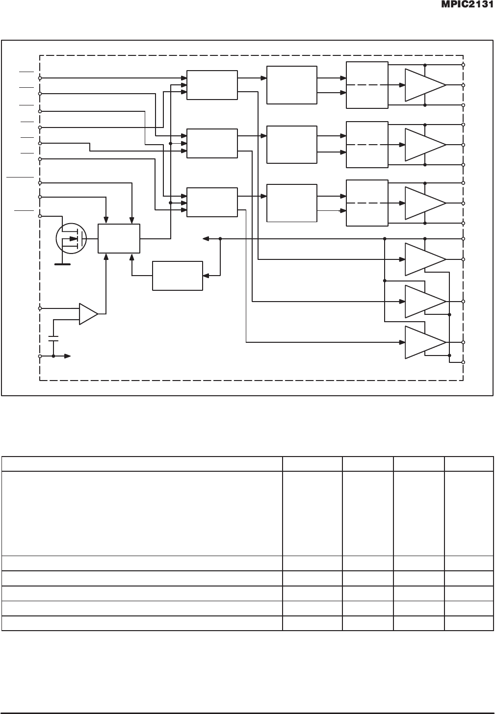
The MPIC2131 is a high voltage, high speed, power MOSFET and IGBT driver
with three independent high side and low side referenced output channels for
3–Phase applications. Proprietary HVIC technology enables ruggedized monolith-
ic construction. Logic inputs are compatible with 5 V CMOS or LSTTL outputs. A
ground referenced operational amplifier provides an analog feedback of bridge
current via an external current sense resistor. A current trip function which termi-
nates all six outputs is also derived from an external current sense resistor. An ex-
tra shutdown input is provided for customizing the shutdown function. An open
drain FAULT signal is provided to indicate that any of shutdown conditions has oc-
curred. The output drivers feature a high pulse current buffer stage designed for
minimum driver cross–conduction. Propagation delays are matched to simplify use
in high frequency applications.
The floating channels can be used to drive N–channel power MOSFET or
IGBT’s in the high side configuration which operate from 10 to 600 volts.
• Floating Channel Designed for Bootstrap Operation
• Fully Operational to +600 V
• Tolerant to Negative Transient Voltage
• dV/dt Immune
• Gate Drive Supply Range from 10 to 20 V
• Undervoltage Lockout for All Channels
• Over–current Shut Down Turns Off All Six Drivers
• Independent 3 High Side & 3 Low Side Drivers
• Matched Propagation Delay for All Channels
• Outputs Out of Phase with Inputs
PRODUCT SUMMARY
V
OFFSET 600
V
MAX
I
O+/– 200
mA/420
mA
V
OUT 10
–
20
V
t
on/off
(typical)
1.4
&
0.7
s
Delay Matching
700
ns
This document contains information on a new product. Specifications and information herein are subject
to change without notice.
REV 1
SEMICONDUCTOR TECHNICAL DATA
Device
Package
3 HIGH SIDE &
3 LOW SIDE
DRIVER
ORDERING INFORMATION
(TOP VIEW)
PIN CONNECTIONS
P SUFFIX
PLASTIC PACKAGE
CASE 710–02
MPIC2131P PDIP
28
1
1
2
3
4
5
6
7
8
22
23
24
25
26
27
28
9
21
20
10
11
12
13
14
17
18
19
16
15
V
CC
HIN1
HIN2
HIN3
LIN1
LIN2
LIN3
FAULT
ITRIP
FLT+CLR
SD
V
SS
COM
LO3
V
B1
HO1
V
S1
V
B2
HO2
V
S2
V
B3
HO3
V
S3
LO1
LO2
4–309
Motorola TMOS Power MOSFET Transistor Device Data
SIMPLIFIED BLOCK DIAGRAM
LATCH
UV
DETECTOR
DRIVER
PULSE
GENERATOR
LEVEL
SHIFTER
SET
RESET
LATCH
UV
DETECTOR
DRIVER
PULSE
GENERATOR
LEVEL
SHIFTER
SET
RESET
LATCH
UV
DETECTOR
DRIVER
SET
RESET
DRIVER
DRIVER
DRIVER
PULSE
GENERATOR
LEVEL
SHIFTER
INPUT
SIGNAL
GENERATOR
INPUT
SIGNAL
GENERATOR
INPUT
SIGNAL
GENERATOR
UNDER–
VOLTAGE
DETECTOR
FAULT
LOGIC
V
CC
V
B3
V
S2
V
S1
V
B1
HO1
H1
L1
H2
L2
H3
L3
CURRENT
COMPARATOR
V
B2
HO2
V
S3
LO1
LO2
LO3
COM
HIN1
HIN2
HIN3
LIN1
LIN2
LIN3
FLT–CLR
V
SS
ITRIP
HO3
0.5 V
SD
FAULT
V
SS
ABSOLUTE MAXIMUM RATINGS
Absolute Maximum Ratings indicate sustained limits beyond which damage to the device may occur. All voltage parameters are absolute
voltages referenced to COM. The Thermal Resistance and Power Dissipation ratings are measured under board mounted and still air
conditions.
Rating
Symbol Min Max Unit
High Side Floating Absolute Voltage
Hi h Sid Fl ti S l Off t V lt
V
B1,2,3
V
–0.3
V25
625
V03
V
DC
High Side Floating Supply Offset Voltage
High Side Floating Out
p
ut Voltage
V
S1,2,3
V
HO123
V
B1,2,3
–25
V
S123
–
0.3
V
B1,2,3
+0.3
V
B123
+0.3
High
Side
Floating
Out ut
Voltage
Low Side Output Voltage
V
HO1
,
2
,
3
V
LO1,2,3
V
S1
,
2
,
3
0
.
3
–0.3
V
B1
,
2
,
3
+0
.
3
V
CC
+0.3
Fixed Supply Voltage
Fixed Su
pp
ly Offset Voltage
,,
V
CC
V
SS
–0.3
V
CC
–
25
25
V
CC
+0 3
Fixed
Su ly
Offset
Voltage
Logic Input Voltage (HIN–, LIN–, FLT–, CLR–, SD & ITRIP)
V
SS
V
IN
V
CC
–
25
V
SS
–0.3
V
CC
+0
.
3
V
CC
+0.3
gg
Fault Output Voltage
IN
FAULT
SS
V
SS
–0.3
CC
V
CC
+0.3
Allowable Offset Supply Voltage Transient dV
S
/dt – 50 V/ns
*Package Power Dissipation @ T
C
≤ +25°C (28 Lead DIP) P
D
– 1.5 Watt
Operating and Storage Temperature T
j
, T
stg
–55 150 °C
Thermal Resistance, Junction to Ambient (8 Lead DIP) R
θJA
– 83 °C/W
Lead Temperature for Soldering Purposes, 10 seconds T
L
– 260 °C

4–310
Motorola TMOS Power MOSFET Transistor Device Data
RECOMMENDED OPERATING CONDITIONS
The Input/Output logic timing Diagram is shown in Figure 1. For proper operation the device should be used within the recommended condi-
tions. The V
S
offset rating is tested with all supplies biased at 15 V differential.
High Side Floating Supply Absolute Voltage
V
B1,2,3
V
S1,2,3
+10 V
S1,2,3
+20 V
High Side Floating Supply Offset Voltage V
S1,2,3
Note 1 V
SO
+600 V
High Side Floating Output Voltage V
HO1,2,3
V
S1,2,3
V
B1,2,3
V
Fixed Supply Voltage V
CC
10 20 V
Low Side Output Voltage V
LO1,2,3
0 V
CC
V
Low Side Driver Return V
SS
–5 5 V
Logic Input Voltage (HIN–, LIN–, FLT–CLR, SD & ITRIP) V
IN
V
SS
5 V
Fault Output Voltage FAULT– V
SS
V
CC
V
Ambient Temperature T
A
–40 125 °C
Note 1: Logic operational for V
S
of –5 V to +600 V. Logic state held for V
S
of –5 V to –V
BS
.
ELECTRICAL CHARACTERISTICS (T
A
= 25°C unless otherwise specified)
Characteristic
Symbol Min Typ Max Unit
STATIC ELECTRICAL CHARACTERISTICS
V
BIAS
(V
CC
, V
BS1,2,3
) = 15 V and V
SS
= COM unless otherwise specified. The V
IN
, V
TH
and I
IN
parameters are referenced to V
SS
and are
applicable to all six channels (HS1,2,3 & LS1,2,3). The VO and IO parameters are referenced to COM and V
SO1,2,3
and are applicable to
the respective output leads: HO1,2,3 or LO1,2,3.
Logic “0” Input Voltage (OUT = LO) V
IH
2.2 – – V
Logic “1” Input Voltage (OUT = HI) V
IL
– – 0.8 V
Logic “0” Fault Clear Input Voltage V
FCLR,IH
2.2 – – V
Logic “1” Fault Clear Input Voltage V
FCLR,IL
– – 0.8 V
SD Input Positive Going Threshold V
SD,TH+
– 1.8 – V
SD Input Negative Going Threshold V
SD,TH–
– 1.5 – V
ITRIP Input Positive Going Threshold V
IT,TH+
– 485 – mV
ITRIP Input Negative Going Threshold V
IT,TH–
– 400 – mV
High Level Output Voltage, V
BIAS
–V
O
@ V
IN
= 0 V, I
O
= 0 A V
OH
– – 100 mV
Low Level Output Voltage, V
O
@ V
IN
= 5 V, I
O
= 0 A V
OL
– – 100 mV
Offset Supply Leakage Current @ V
B1,2,3
= V
S1,2,3
= 600 V I
LK
– – 50 µA
Quiescent V
BS
Supply Current @ V
IN
= 0 V or 5 V I
QBS
– 30 – µA
Quiescent V
CC
Supply Current @ V
IN
= 0 V or 5 V I
QCC
– 3.0 – mA
Logic “1” Input Bias Current (OUT = HI) @ V
IN
= 0 V I
IN+
– 190 – µA
Logic “0” Input Bias Current (OUT = LO) @ V
IN
= 5 V I
IN–
– 100 – µA
“High” ITRIP Bias Current @ ITRIP = 5 V I
TRIP+
– 60 – µA
“Low” ITRIP Bias Current @ ITRIP = 0 V I
TRIP–
– – 50 nA
Logic “1” Fault Clear Bias Current @ FLT–CLR = 0 V I
FCLR+
– 190 – µA
Logic “0” Fault Clear Bias Current @ FLT–CLR = 5 V I
FCLR–
– 100 – µA
Logic “1” Shut Down Bias Current @ SD = 5 V I
SD+
– 60 – µA
Logic “0” Shut Down Bias Current @ SD = 5 V I
SD–
– – 150 nA
V
BS
Supply Undervoltage Positive Going Threshold V
BSUV+
– 8.6 – V
V
BS
Supply Undervoltage Negative Going Threshold V
BSUV–
– 8.2 – V
V
CC
Supply Undervoltage Positive Going Threshold V
CCUV+
– 9.0 – V
V
CC
Supply Undervoltage Negative Going Threshold V
CCUV–
– 8.7 – V
FAULT – Low On Resistance R
on,FLT
– 55 – Ω
Output High Short Circuit Pulsed Current @ V
out
= 0 V, V
in
= 0 V, PW ≤ 10 µs I
O+
200 250 – mA
Output Low Short Circuit Pulsed Current @ V
out
= 15 V, V
in
= 5 V, PW ≤ 10 µs I
O–
420 500 – mA
4–311
Motorola TMOS Power MOSFET Transistor Device Data
ELECTRICAL CHARACTERISTICS (T
A
= 25°C unless otherwise specified)
Characteristic Symbol Min Typ Max Unit
DYNAMIC ELECTRICAL CHARACTERISTICS
V
BIAS
(V
CC
, V
BS1,2,3
) = 15 V, V
SO1,2,3
= V
SS
and C
L
= 1000 pF unless otherwise specified. T
A
= 25°C.
Turn–On Propagation Delay @ V
IN
= 0 & 5 V, V
S1,2,3
= 0 V to 600 V t
on
– 1.4 – µs
Turn–Off Propagation Delay @ V
IN
= 0 & 5 V, V
S1,2,3
= 0 V to 600 V t
off
– 0.7 – µs
Turn–On Rise Time @ V
IN
= 0 & 5 V, V
S1,2,3
= 0 V to 600 V t
r
– 80 – ns
Turn–On Fall Time @ V
IN
= 0 & 5 V, V
S1,2,3
= 0 V to 600 V t
f
– 40 – ns
ITRIP to Output Shutdown Propagation Delay @ V
IN
, V
ITRIP
= 0 & 5 V t
itrip
– 550 – ns
ITRIP Blanking Time @ ITRIP = 1 V t
bl
– 400 – ns
ITRIP to FAULT– Propagation Delay @ V
IN
, V
ITRIP
= 0 & 5 V t
flt
– 450 – ns
Input Filter Time (all six inputs) @ V
IN
= 0 & 5 V t
flt,in
– 310 – ns
FLT–CLR to FAULT Clear Time @ V
IN
, V
IT
, V
FC
= 0 & 5 V t
fltclr
– 450 – ns
SD to OUTPUT Shutdown Propagation Delay @ V
IN
, V
SD
= 0 & 5 V t
sd
– 550 – ns
Deadtime, LS Turn–Off to HS Turn–On & HS Turn–Off to LS Turn–On
@ V
IN
= 0 & 5 V
DT – 700 – ns
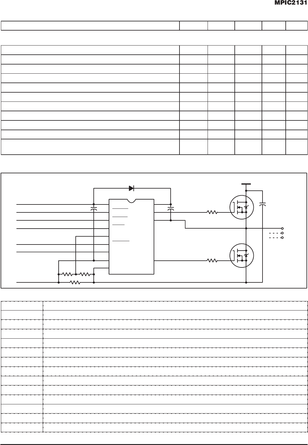
TYPICAL CONNECTION
10 TO 600 V
TO
LOAD
V
CC
ITRIP
COM
V
B1,2,3
HIN1,2,3
V
SS
SD
FLT–CLR
LIN1,2,3
FAULT
HO1,2,3
V
S1,2,3
LO1,2,3
LEAD DEFINITIONS
Symbol Lead Description
HIN1,2,3 Logic Inputs for High Side Gate Driver Outputs (HO1,2,3), Out of Phase
LIN1,2,3 Logic Inputs for Low Side Gate Driver Outputs (LO1,2,3), Out of Phase
FLT–CLR Logic Inputs for Fault Clear
SD Logic Input for Shut Down
FAULT Indicates Over–current, Shut Down or Low Side Undervoltage Condition, Negative Logic
ITRIP Input for Over–current Shut Down
V
SS
Logic Ground
V
B1,2,3
High Side Floating Supplies
HO1,2,3 High Side Gate Drive Outputs
V
S1,2,3
High Side Floating Supply Returns
V
CC
Logic and Low Side Fixed Supply
LO1,2,3 Low Side Gate Drive Outputs
COM Low Side Return
4–312
Motorola TMOS Power MOSFET Transistor Device Data
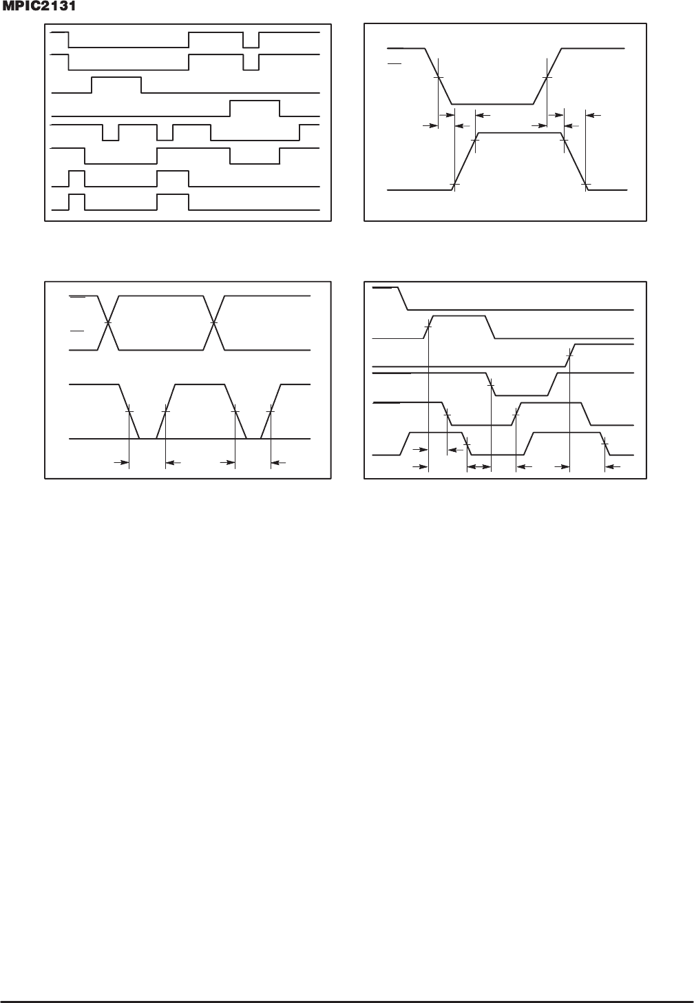
Figure 1. Input / Output Timing Diagram
Figure 2. Switching Time Waveform
Definitions
Figure 3. Deadtime Waveform Definitions
LO
HO
HIN
LIN
50% 50%
50% 50%
DT DT
HIN
LIN
ITRIP
FAULT
HO
LO
HIN
LIN
LO
HO
50% 50%
10% 10%
90% 90%
t
on
t
r
t
off
t
f
50%
50%
50%
50%
50%
t
flt
LO2
FAULT
ITRIP
LIN2
t
itrip
t
fltclr
Figure 4. Shutdown Waveform Definitions
FLT–CLR
SD
SD
FLT–CLR
t
sd
50%
50%
4–313
Motorola TMOS Power MOSFET Transistor Device Data
Power Products Division
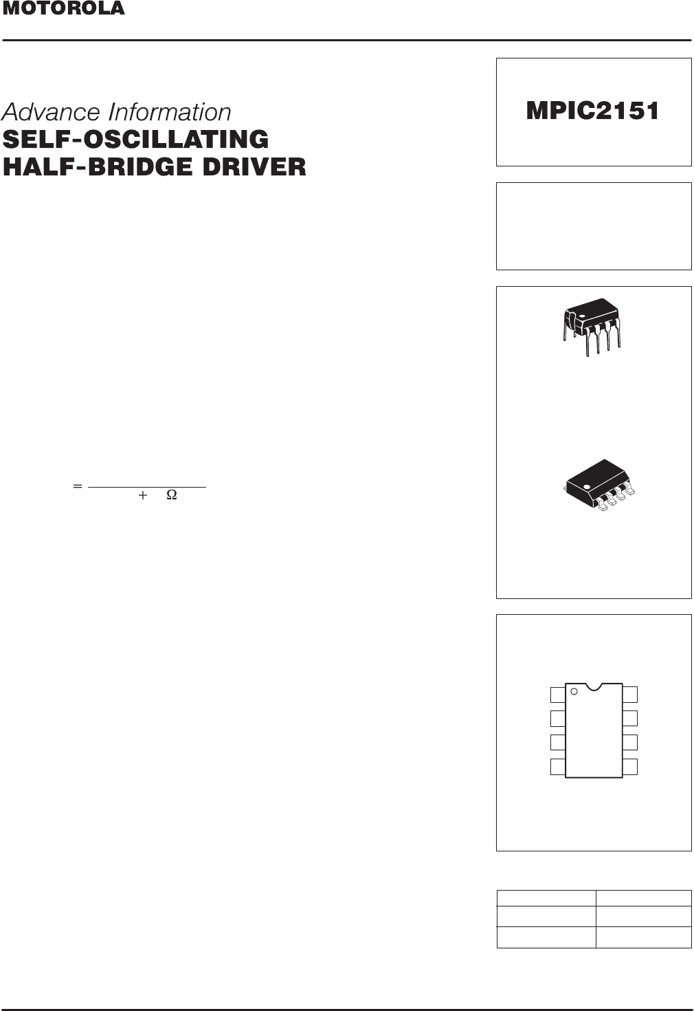
The MPIC2151 is a high voltage, high speed, self–oscillating power MOSFET
and IGBT driver with both high side and low side referenced output channels. Pro-
prietary HVIC and latch immune CMOS technologies enable ruggedized monolith-
ic construction. The front–end features a programmable oscillator which is similar
to the 555 timer. The output drivers feature a high pulse current buffer stage and an
internal deadtime designed for minimum driver cross–conduction. Propagation de-
lays for the two channels are matched to simplify use in 50% duty cycle applica-
tions. The floating channel can be used to drive an N–channel power MOSFET or
IGBT in the high side configuration that operates off a high voltage rail from 10 to
600 volts.
• Floating Channel Designed for Bootstrap Operation
• Fully Operational to +600 V
• Tolerant to Negative Transient Voltage
• dV/dt Immune
• Undervoltage Lockout
• Programmable Oscillator Frequency:
f
1
1.4 (RT 75 )CT
• Matched Propagation Delay for Both Channels
• Low Side Output In Phase with RT
PRODUCT SUMMARY
V
OFFSET 600
V
MAX
Duty Cycle
50%
V
OUT 10
–
20
V
t
r/f
(typical) 120 & 60 ns
Deadtime (typical) 1.2 µs
This document contains information on a new product. Specifications and information herein are subject
to change without notice.
REV 1
SEMICONDUCTOR TECHNICAL DATA
Device
Package
SELF–OSCILLATING
HALF–BRIDGE
DRIVER
ORDERING INFORMATION
MPIC2151P PDIP
D SUFFIX
PLASTIC PACKAGE
CASE 751–05
(SO–8)
8
1
(TOP VIEW)
PIN CONNECTIONS
P SUFFIX
PLASTIC PACKAGE
CASE 626–05
8
1
MPIC2151D SOIC
V
B
8V
CC
RT
CT
COM
HO
V
S
LO
7
6
5
1
2
3
4
4–314
Motorola TMOS Power MOSFET Transistor Device Data
SIMPLIFIED BLOCK DIAGRAM
PULSE
GEN
PULSE
FILTER
HV
LEVEL
SHIFT
COM
LO
V
CC
V
S
V
B
HO
R
S
Q
DELAY
DEAD
TIME
DEAD
TIME
UV
DETECT
+
–
+
–
R
R
R
RT
CT
R
S
Q
Q
15.6 V
ABSOLUTE MAXIMUM RATINGS
Absolute Maximum Ratings indicate sustained limits beyond which damage to the device may occur. All voltage parameters are absolute
voltages referenced to COM, all currents are defined positive into any lead. The Thermal Resistance and Power Dissipation ratings are
measured under board mounted and still air conditions.
Rating
Symbol Min Max Unit
Hi
g
h Side Floatin
g
Suppl
y
Absolute Volta
g
e V
B
–0.3 625 V
DC
High
Side
Floating
Su ly
Absolute
Voltage
Hi
g
h Side Floatin
g
Suppl
y
Offset Volta
g
e
V
B
V
S
0.3
V
B
–25
625
V
B
+0.3
V
DC
ggyg
High Side Floating Output Voltage
S
V
HO
B
V
S
–0.3
B
V
B
+0.3
ggg
Low Side Output Voltage
HO
V
LO
S
–0.3
B
V
CC
+0.3
g
RT Voltage
LO
V
RT
–0.3
CC
V
CC
+0.3
CT Voltage V
CT
–0.3 V
CC
+0.3
Supply Current (Note 1) I
CC
– 25 mA
DC
y()
High Side Output Current
CC
I
HO
–500 500
DC
Low Side Output Current
RT O t t C t
I
LO
I
–500
50
500
50
RT Output Current I
RT
–5.0 5.0
Allowable Offset Supply Voltage Transient dV
S
/dt – 50 V/ns
*Package Power Dissipation @ T
C
≤ +25°C (8 Lead DIP)
(8 Lead SOIC)
P
D
–
–
–
1.0
0.625
Watt
Operating and Storage Temperature T
j
, T
stg
–55 150 °C
Thermal Resistance, Junction to Ambient (8 Lead DIP)
(8 Lead SOIC)
R
θJA
–
–
125
200
°C/W
Lead Temperature for Soldering Purposes, 10 seconds T
L
– 260 °C
RECOMMENDED OPERATING CONDITIONS
The Input/Output logic timing Diagram is shown in Figure 1. For proper operation the device should be used within the recommended condi-
tions.
High Side Floating Supply Absolute Voltage
V
B
V
S
+10 V
S
+V
clamp
V
High Side Floating Supply Offset Voltage V
S
– 600
High Side Floating Output Voltage V
HO
V
S
V
B
Low Side Output Voltage V
LO
0 V
CC
Supply Current (Note 1) I
CC
– 5.0 mA
Ambient Temperature T
A
–40 125 °C
Note 1: Because the MPIC2151 is designed specifically for off–line supply systems, this IC contains a zener clamp structure between the chip
V
CC
and COM which has a nominal breakdown voltage of 15.6 V. Therefore, the IC supply voltage is normally derived by forcing current into
the supply lead (typically by means of a high value resistor connected between the chip V
CC
and the rectified line voltage and a local decoup-
ling capacitor from V
CC
to COM) and allowing the internal zener clamp circuit to determine the nominal supply voltage. Therefore, this circuit
should not be driven by a DC, low impedance power source of greater than V
CLAMP
.

4–315
Motorola TMOS Power MOSFET Transistor Device Data
ELECTRICAL CHARACTERISTICS (T
C
= 25°C unless otherwise specified)
Characteristic Symbol Min Typ Max Unit
STATIC ELECTRICAL CHARACTERISTICS
Supply Characteristics
V
BIAS
(V
CC
, V
BS
) = 12 V, V
SS
= COM and C
L
= 1000 pF unless otherwise specified.
V
CC
Supply Undervoltage Positive Going Threshold
V
CCUV+
– 8.4 –
V
DC
V
CC
Supply Undervoltage Negative Going Threshold V
CCUV–
– 8.0 –
Quiescent V
CC
Supply Current I
QCC
– 400 – µA
V
CC
Zener Shunt Clamp Voltage @ I
OC
= 5 mA V
CLAMP
– 15.6 – V
DC
Floating Supply Characteristics
Offset Supply Leakage Current @ V
B
= V
S
= 600 V I
LK
– – 50
µA
DC
Quiescent V
BS
Supply Current I
QBS
– 10 –
Oscillator I/O Characteristics
Oscillator Frequency @ RT = 35.7 KΩ, CT = 1 nF f
OSC
– 20 –
kHz
Oscillator Frequency @ RT = 7.04 KΩ, CT = 1 nF f
OSC
– 100 –
CT Input Current I
CT
– 0.001 1.0 µA
CT Undervoltage Lockout @ 2.5 V < V
CC
< V
CCUV+
V
CTUV
– 0 –
mV
RT High Level Output Voltage, V
CC
– RT @ IRT = –100 µA
@ IRT = –1 mA
V
RT+
V
RT+
–
–
20
200
–
–
RT Low Level Output Voltage, V
CC
+ RT @ IRT = 100 µA
@ IRT = 1 mA
V
RT–
V
RT–
–
–
20
200
–
–
RT Undervoltage Lockout, V
CC
– RT @ 2.5 V < V
CC
< V
CCUV+
V
RTUV
– 0 –
2/3 V
CC
Threshold V
CT+
– 8.0 –
V
DC
1/3 V
CC
Threshold V
CT–
– 4.0 –
Output Characteristics
High Level Output Voltage, V
BIAS
–V
O
@ I
O
= 0 A V
OH
– – 100
mV
Low Level Output Voltage, V
O
@ I
O
= 0 A V
OL
– – 100
Dynamic Electrical Characteristics
V
BIAS
(V
CC
, V
BS
) = 12 V and C
L
= 1000 pF unless otherwise specified. T
A
= 25°C.
Turn–On Rise Time t
r
– 120 –
ns
Turn–Off Fall Time t
f
– 60 –
Deadtime, LS Turn–Off to HS Turn–On & HS Turn–Off to LS Turn–On DT – 1.2 – µA
RT Duty Cycle, f
OSC
= 20 kHz DC – 50 – %
4–316
Motorola TMOS Power MOSFET Transistor Device Data
TYPICAL CONNECTION
TO
LOAD
10 TO 600 V
V
CC
RT
COM
V
B
CT
HO
V
S
LO
LEAD DEFINITIONS
Symbol Lead Description
RT Oscillator timing resistor input; a resistor is connected from RT to CT. RT is in phase with LO for normal IC operation.
CT Oscillator timing capacitor input; a capacitor is connected from CT to COM in order to program the oscillator frequency
according to the following equation:
where 75Ω is the effective impedance of the R
T
output stage.
V
B
High Side Floating Supply
HO High Side Gate Drive Output
V
S
High Side Floating Supply Return
V
CC
Logic and Low Side Fixed Supply
LO Low Side Gate Drive Output
COM Logic and Low Side Return
Figure 1. Input / Output Timing Diagram
Figure 2. Switching Time Waveform Definitions
Figure 3. Deadtime Waveform Definitions
LO
HO
V
CLAMP
V
CCUV+
V
CC
RT
CT
RT(HO)
RT(LO)
LO
HO
50% 50%
10% 10%
90% 90%
t
r
t
f
50%50%
RT
HO
LO
90%
90%
10%
10%
DT
f
1
1.4 (RT 75 )CT
4–317
Motorola TMOS Power MOSFET Transistor Device Data
N–Channel Enhancement–Mode Silicon Gate
The D
2
PAK package has the capability of housing a larger die
than any existing surface mount package which allows it to be used
in applications that require the use of surface mount components
with higher power and lower R
DS(on)
capabilities. This high voltage
MOSFET uses an advanced termination scheme to provide
enhanced voltage–blocking capability without degrading perfor-
mance over time. In addition, this advanced TMOS E–FET is
designed to withstand high energy in the avalanche and commuta-
tion modes. The new energy efficient design also offers a
drain–to–source diode with a fast recovery time. Designed for high
voltage, high speed switching applications in power supplies,
converters and PWM motor controls, these devices are particularly
well suited for bridge circuits where diode speed and commutating
safe operating areas are critical and offer additional safety margin
against unexpected voltage transients.
• Robust High Voltage Termination
• Avalanche Energy Specified
• Source–to–Drain Diode Recovery Time Comparable to a
Discrete Fast Recovery Diode
• Diode is Characterized for Use in Bridge Circuits
• I
DSS
and V
DS(on)
Specified at Elevated Temperature
• Short Heatsink Tab Manufactured — Not Sheared
• Specially Designed Leadframe for Maximum Power Dissipation
• Available in 24 mm 13–inch/800 Unit Tape & Reel, Add T4 Suffix to Part Number
MAXIMUM RATINGS
(T
C
= 25°C unless otherwise noted)
Rating
Symbol Value Unit
Drain–Source Voltage V
DSS
1000 Vdc
Drain–Gate Voltage (R
GS
= 1.0 MΩ) V
DGR
1000 Vdc
Gate–Source Voltage — Continuous
Gate–Source Voltage — Non–Repetitive (t
p
≤ 10 ms)
V
GS
V
GSM
± 20
± 40
Vdc
Vpk
Drain Current — Continuous
Drain Current — Continuous @ 100°C
Drain Current — Single Pulse (t
p
≤ 10 µs)
I
D
I
D
I
DM
1.0
0.8
3.0
Adc
Apk
Total Power Dissipation
Derate above 25°C
Total Power Dissipation @ T
A
= 25°C, when mounted with the minimum recommended pad size
P
D
75
0.6
2.5
Watts
W/°C
Watts
Operating and Storage Temperature Range T
J
, T
stg
– 55 to 150 °C
Single Pulse Drain–to–Source Avalanche Energy — Starting T
J
= 25°C
(V
DD
= 25 Vdc, V
GS
= 10 Vdc, I
L
= 3.0 Apk, L = 10 mH, R
G
= 25 Ω)
E
AS
45 mJ
Thermal Resistance — Junction to Case
Thermal Resistance — Junction to Ambient
Thermal Resistance — Junction to Ambient, when mounted with the minimum recommended pad size
R
θJC
R
θJA
R
θJA
1.67
62.5
50
°C/W
Maximum Lead Temperature for Soldering Purposes, 1/8″ from case for 10 seconds T
L
260 °C
Designer’s Data for “Worst Case” Conditions — The Designer’s Data Sheet permits the design of most circuits entirely from the information presented. SOA Limit
curves — representing boundaries on device characteristics — are given to facilitate “worst case” design.
Preferred devices are Motorola recommended choices for future use and best overall value.
SEMICONDUCTOR TECHNICAL DATA
TMOS POWER FET
1.0 AMPERES
1000 VOLTS
R
DS(on)
= 9.0 OHM
Motorola Preferred Device
CASE 418B–02, Style 2
D
2
PAK
D
S
G
REV 2