Yellampalli S. (ed.) Carbon Nanotubes - Synthesis, Characterization, Applications
Подождите немного. Документ загружается.

Dielectrophoretic Deposition and Alignment of Carbon Nanotubes
177
These equations indicate that the dielectrophoresis of CNTs is affected by many factors
including the dimensions of the nanotubes, the properties of the medium, and the strength
of the electric field. In our investigation, the following parameters are adjusted to control the
deposition and alignment of the nanotubes: bias voltage, frequency, deposition time, width
of the electrodes, and nanotube solution concentration.
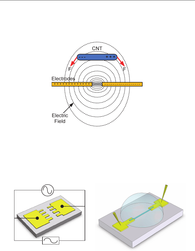
Fig. 7. Principle of dielectrophoresis deposition and alignment of a carbon nanotube.
Early research demonstrates that the polarization along the longitudinal direction is much
higher than that along the transverse direction for metallic CNTs, but comparable for
semiconducting CNTs (Padmaraj et al., 2009). This is because the metallic CNTs have a
larger
Re[f
cm
] and the dielectrophoretic force exerted on them is much stronger than that
experienced by the semiconducting CNTs. Therefore, we expect that the metallic CNTs will
dominate the movement of SWNT bundles in the dielectrophoresis process in our
experiments.
Fig. 8. (a) Experimental system for the dielectrophoresis of CNTs. (b) Schematic diagram of
the CNT alignment. Reprinted with permission from P. Li & Xue, 2010a. @ 2010 Springer.
Figure 8a shows the configuration of the experimental system for the dielectrophoresis of
the CNTs. A function generation (Agilent Technologies 81150A) is used as the AC signal
(a)
AC Source
Oscilloscope
(b)

Carbon Nanotubes - Synthesis, Characterization, Applications
178
source and it is connected to the electrodes through two metal probes. The potential drop
across the electrode gap is monitored with an oscilloscope (Agilent Technologies MSO
7054A), which provides the voltage value in real time. After the instruments are set up, a
droplet of the CNT solution is carefully placed in the area between the electrodes with a
syringe. Next, the AC signal source is switched on. An electric field is generated in between
the electrode “teeth“. The electric field exerts dielectrophoretic forces on the CNTs and
forces them to rotate along the field lines. The CNTs can be deposited on the substrate with
this orientation, as shown in Fig. 8b. After 30 sec of dielectrophoresis, the AC signal is
switched off and the CNT solution is removed with another syringe. The experiments are
conducted at room temperature with an applied AC signal with a peak-to-peak voltage of
V
pp
= 10 V and frequency of f = 5 MHz.
4. Results and discussion
In the dielectrophoresis process, the dielectrophoretic forces drag the CNTs to the gap of the
electrodes where the electric field has the highest magnitude. In reality, however, the
dielectrophoresis process and the deposition results of the CNTs are affected by a number of
factors including the dimensions of the nanotubes, the properties of the medium, and the
strength of the electric field. In this research, the alignment results of the two forms of
CNTs—SWNTs and MWNTs—are investigated and compared. In addition, the electrical
properties of these resulting CNTs are studied.
4.1 SWNTs
As described earlier, the fabricated devices can be divided into three groups: 400-μm-wide
electrodes, 5-μm-wide electrodes, and 3-μm-wide electrodes. For each group, the electrodes
are exposed to the SWNT solutions with different concentrations, ranging from 0.2 to
0.00125 mg/ml. An SEM (FEI Quanta 3D 200i) is used to inspect the deposited SWNTs after
the dielectrophoresis process. A semiconductor device analyzer (Agilent Technologies
B1500A) is used to characterize the electrical properties of the aligned SWNTs.
4.1.1 Deposition and alignment of the SWNTs
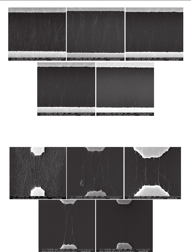
Figure 9 shows the SEM images of the deposited SWNTs on the substrates with the 400-μm-
wide electrodes. This electrode design enables an evenly distributed electric field with
parallel field lines in the gap. The SWNTs are stretched and aligned in between the
electrodes to follow the parallel field lines. The density of the SWNT thin film is dependent
on the concentration of the SWNT solution used in the dielectrophoresis process. A higher
solution concentration induces a denser SWNT film. The alignment experiments are highly
repeatable when used to fabricate SWNT thin films. However, it is difficult to obtain small
nanotube bundles or individual nanotubes using this group of devices.
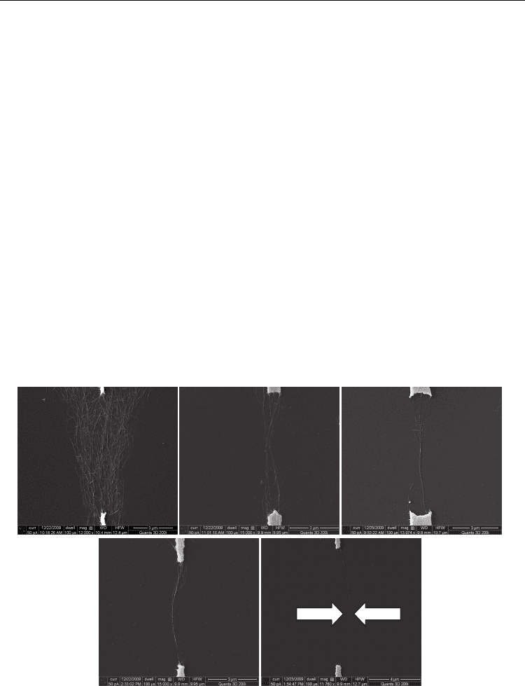
In order to explore the possibility of producing aligned nanotube bundles and individual
nanotubes, narrower electrodes are used. Figure 10 shows the SEM images of the aligned
SWNTs on the devices with the 5-μm-wide electrodes. Figure 10a demonstrates a dense film
of SWNTs covering the electrode gap, where most SWNTs are aligned to follow the
direction of the electric field lines. As the solution concentration decreases, fewer SWNTs
are attracted by the dielectrophoretic force and deposited on the substrate. In addition, the
SEM inspection shows that there are no SWNTs observed outside the electrode gap area.
Dielectrophoretic Deposition and Alignment of Carbon Nanotubes
179
Fig. 9. SEM images of aligned SWNTs with the 400-μm-wide electrodes and solutions with
different concentrations: (a) 0.2 mg/ml, (b) 0.1 mg/ml, (c) 0.05 mg/ml, (d) 0.025 mg/ml, and
(e) 0.0125 mg/ml. Reprinted with permission from P. Li & Xue, 2010a. @ 2010 Springer.
Fig. 10. SEM images of aligned SWNTs with the 5-μm-wide electrodes and solutions with
different concentrations: (a) 0.2 mg/ml, (b) 0.1 mg/ml, (c) 0.05 mg/ml, (d) 0.025 mg/ml, and
(e) 0.0125 mg/ml. Reprinted with permission from P. Li & Xue, 2010a. @ 2010 Springer.
(a)
(d)
(e)
(b)
(c)
(a)
(b)
(c)
(d)
(e)
Carbon Nanotubes - Synthesis, Characterization, Applications
180
This proves that the dielectrophoresis process is a selective deposition technique which only
moves SWNTs to areas with strong electric fields. Figure 10b-d show sparsely distributed
nanotube bundles and Fig. 10e shows a small bundle of SWNTs. Compared with the devices
with wider electrodes (Fig. 9), the devices with 5-μm-wide electrodes can generate a more
concentrated electric field in the gap and force the SWNTs to land on the substrate to cover a
smaller area. The bundling phenomenon of the SWNTs in the solution is caused by their
high aspect ratios and high flexibility. Based on Fig. 10b-e, as the solution concentration
decreases, the bundles become thinner due to the lower availability of SWNTs in the
solution.
For the narrowest electrodes with the width of 3 μm, the quality of the deposition and
alignment of SWNTs is similar to that for the electrodes with 5-μm width, as shown in Fig.
11. However, there are three major differences comparing the results from the two designs.
First, the amount of the aligned SWNTs on the 3-μm-wide electrodes is smaller. This is
because the area with a strong and concentrated electric field, generated by the narrower
electrodes, is smaller. Second, the bundles deposited on the 3-μm-wide electrodes are
thinner and contain smaller numbers of nanotubes. Third, and most importantly, individual
nanotubes can be observed in the dielectrophoresis experiments using low-concentration
solutions and 3-μm-wide electrodes (Fig. 11e). In this case, the narrow electrode design
ensures that the electric field in between the electrodes is extremely concentrated and highly
directional. The low solution concentration ensures that in the adjacent area there is only
one nanotube available in the solution to be attracted by the electric field. Consequently, this
individual nanotube is deposited on the substrate and aligned in between the electrodes.
Fig. 11. SEM images of aligned SWNTs with the 3-μm-wide electrodes and solutions with
different concentrations: (a) 0.2 mg/ml, (b) 0.1 mg/ml, (c) 0.05 mg/ml, (d) 0.025 mg/ml, and
(e) 0.0125 mg/ml. Reprinted with permission from P. Li & Xue, 2010a. @ 2010 Springer.
(b)
(a) (c)
(d)
(e)
Dielectrophoretic Deposition and Alignment of Carbon Nanotubes
181
4.1.2 Electrical characteristics of the aligned SWNTs
After the dielectrophoresis process, the gap of the electrodes are covered with the deposited
and aligned SWNTs, which allows the transmission of electric charges across the electrodes.
As a result, these devices can be measured as regular resistors with the electrodes as the
testing pads and the aligned SWNTs as the conductive path (P. Li & Xue, 2010b). To gain a
better understanding of the effects of the solution concentration on the deposition and
alignment of SWNTs, the electrical properties of the devices after the dielectrophoresis
process are characterized with the semiconductor device analyzer. Based on the design of
the electrodes, the devices are divided into two groups: the first group contains devices with
the wide electrodes (width: 400 μm) and the second group includes devices with the “teeth“-
like electrodes (width: 5 μm and 3 μm). Each group consists of five different SWNT devices
corresponding to the solutions used in the dielectrophoresis process.
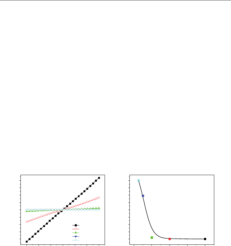
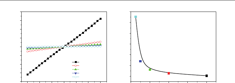
The electrical properties of the wide-electrode devices are illustrated in Fig. 12a. The width
and the gap of the electrodes are 400 and 5 μm, respectively. These devices are measured as
regular resistors with the current-voltage plots as the output characteristics. In the measured
range of -3 to 3 V, all plots are highly linear. The resistances of these devices are calculated
accordingly and plotted in Fig. 12b. At a low SWNT solution concentration of 0.0125 mg/ml,
which corresponds to the device shown in Fig. 9e, only a few SWNTs are captured. The
resistance is measured as approximately 35.015 kΩ. As the concentration increases, the
resistance quickly decreases to a lower value and remains relatively constant in a low-
resistance region. The calculated resistances are 23.641 kΩ (SWNT solution: 0.025 mg/ml),
0.832 kΩ (SWNT solution: 0.05 mg/ml), 0.099 kΩ (SWNT solution: 0.1 mg/ml), and 0.035 kΩ
(SWNT solution: 0.2 mg/ml).
Fig. 12. (a) Current-voltage plots of five devices with the 400-μm-wide electrodes using
SWNT solutions with different concentrations. (b) Resistance as a function of the
concentration for the aligned SWNTs. The resistances are calculated from (a). Reprinted
with permission from P. Li & Xue, 2010b. @ 2010 American Society of Mechanical Engineers.
The electrical characteristics of the devices with the “teeth”-like electrodes are obtained
using the same method. The devices are based on the second electrode design which
contains electrodes with variable widths (Fig. 4). Each device consists of eleven 5-μm-wide
electrode pairs and nine 3-μm-wide electrode pairs. Figure 13a shows the
I-V plots of five
devices using SWNT solutions with five different concentrations. In the measured range of -
3 and 3 V, all five
I-V plots are highly linear. Figure 13b shows the calculated resistance as a
(a)
(b)
-3 -2 -1 0 1 2 3
-80
-60
-40
-20
0
20
40
60
80
Current (mA)
Voltage (V)
Wide Electrodes
SWNT Concentration:
0.2 mg/ml
0.1 mg/ml
0.05 mg/ml
0.025 mg/ml
0.0125 mg/ml
0.00 0.05 0.10 0.15 0.20
0
4
8
12
16
20
24
28
32
Wide Electrodes
SWNT Devices
Resistance (k)
Concentration (mg/ml)
Carbon Nanotubes - Synthesis, Characterization, Applications
182
Fig. 13. (a) Current-voltage plots of five devices with the “teeth”-like electrodes using SWNT
solutions with different concentrations. (b) Resistance as a function of the concentration for
the aligned SWNTs. The resistances are calculated from (a). Reprinted with permission from
P. Li & Xue, 2010a. @ 2010 Springer.
function of the solution concentration. The resistance of the device starts as 11.055 kΩ at the
lowest concentration (SWNT solution: 0.0125 mg/ml) and quickly decreases to 2.806 kΩ
(SWNT solution: 0.025 mg/ml). It continues to decrease to lower values of 1.256 kΩ (SWNT
solution: 0.05 mg/ml), 0.571 kΩ (SWNT solution: 0.1 mg/ml), and 0.097 kΩ (SWNT solution:
0.2 mg/ml). Although this group of devices shows a similar resistance-concentration
relationship to the first group of devices with wide electrodes, the resistance range is
different. For example, the largest obtained resistances are 11.055 and 32.015 kΩ for the
“teeth”-like and wide electrodes, respectively. This difference is caused by the different
amount of aligned SWNTs on the substrates. The devices with wide electrodes are able to
capture more SWNTs, providing more conductive paths for the charges to move across the
electrodes. As a result, these devices show lower resistance.
The characterization of these devices verifies the results from the SEM inspection and
proves that the higher-concentration solutions lead to denser films with more deposited
SWNTs. The high linearity of the
I-V plots suggests that the aligned SWNTs are mostly
metallic nanotubes instead of semiconducting nanotubes. These experimental results fit well
with the prediction described in Section 3: Dielectrophoresis.
4.2 MWNTs
The deposition, alignment, and electrical characteristics of the MWNTs are investigated
using the same procedures as those for the SWNTs. The experiment and measurement
results of the aligned MWNTs are described; the main differences between the deposited
MWNTs and SWNTs are discussed.
4.2.1 Deposition and alignment of the MWNTs
The alignment results of the MWNTs are similar to those for the SWNTs – the solutions with
higher MWNT concentrations generate denser films, as shown in Fig. 14. However, most
MWNTs are tangled together and are not fully stretched in between the electrodes. This can
be explained by the special dimensions and structures of the MWNTs. First, the typical
diameter of the MWNTs used in our experiments is 60-100 nm, which is much larger than
0.00 0.05 0.10 0.15 0.20
0
2
4
6
8
10
12
"Teeth"-like Electrodes
SWNT Devices
Resistance (k)
Concentration (mg/ml)
-3 -2 -1 0 1 2 3
-40
-30
-20
-10
0
10
20
30
40
Current (mA)
Voltage (V)
"Teeth"-like Electrodes
SWNT Concentration:
0.2 mg/ml
0.1 mg/ml
0.05 mg/ml
0.025 mg/ml
0.0125 mg/ml
(a) (b)
Dielectrophoretic Deposition and Alignment of Carbon Nanotubes
183
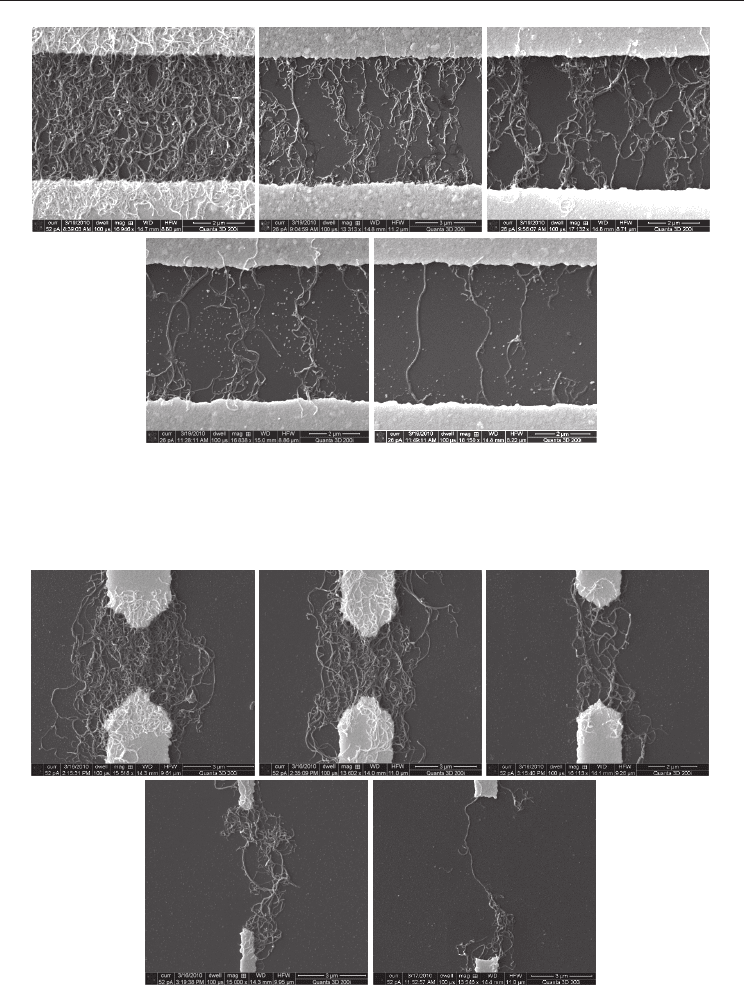
Fig. 14. SEM images of aligned MWNTs with the 400-μm-wide electrodes and solutions with
different concentrations: (a) 0.1 mg/ml, (b) 0.05 mg/ml, (c) 0.025 mg/ml, (d) 0.0125 mg/ml,
and (e) 0.00625 mg/ml.
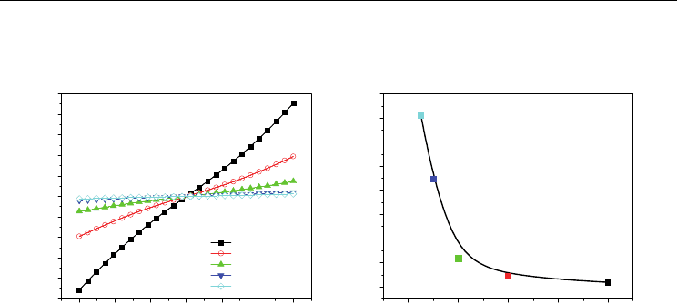
Fig. 15. SEM images of aligned MWNTs with the “teeth”-like electrodes and solutions with
different concentrations: (a) 0.1 mg/ml, (b) 0.05 mg/ml, (c) 0.025 mg/ml, (d) 0.0125 mg/ml,
and (e) 0.00625 mg/ml.
(b)
(a) (c)
(d)
(e)
(b)
(a) (c)
(d)
(e)
Carbon Nanotubes - Synthesis, Characterization, Applications
184
that of the SWNTs (2 nm). Second, the multi-walled structure of the MWNTs makes their
mechanical properties different from the SWNTs – the MWNTs are heavier and stiffer. As a
result, when the MWNTs are exposed to an external electric field, the generated
dielectrophoretic forces are not strong enough to fully stretch the MWNTs. Furthermore, the
thin films generated from the solutions with higher MWNT concentrations have a higher
degree of randomness. As the concentration decreases to a lower level, the MWNTs are
suspended in the solution more homogeneously and their interaction with each other
becomes weaker. Therefore, the resulting films and bundles are more organized with better
quality of alignment.
The “teeth”-like electrodes are also used for the dielectrophoretic assembly of the
MWNTs, as shown in Fig. 15. Unlike the wide electrodes, the “teeth”-like electrodes only
generate high-gradient electric field between two opposite “teeth”. Consequently, the
MWNTs are only deposited in these locations. Similar to the experimental results of the
SWNT samples, the MWNTs only deposit in between the electrodes. In addition, we are
able to achieve not only the deposition of narrow-width thin films, but also the assembly
of a controlled amount of MWNTs or even individual MWNTs, as demonstrated in
Fig. 15e.
4.2.2 Electrical characteristics of the aligned MWNTs
The electrical characterization of the MWNTs deposited on the electrodes is performed after
the dielectrophoresis process. The devices are divided into two groups: the first group
contains devices with the wide electrodes (width: 400 μm) and the second group includes
devices with the “teeth“-like electrodes. Each group consists of five different MWNT devices
corresponding to the solutions used in the dielectrophoresis process.
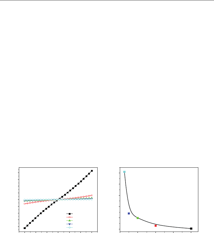
Fig. 16. (a) Current-voltage plots of five devices with the 400-μm-wide electrodes using
MWNT solutions with different concentrations. (b) Resistance as a function of the
concentration for the aligned MWNTs. The resistances are calculated from (a). Reprinted
with permission from P. Li & Xue, 2010b. @ 2010 American Society of Mechanical Engineers.
Figure 16 shows the
I-V plots and the resistance-concentration function of the five MWNT
devices with the wide electrodes. The MWNT thin films behave in a similar way to the
SWNT thin films. At a low MWNT concentration of 0.00625 mg/ml, the resistance is
measured as 20.433 kΩ. As the solution concentration increases, the resistance decreases to
(a)
(b)
-3 -2 -1 0 1 2 3
-20
-15
-10
-5
0
5
10
15
20
Current (mA)
Voltage (V)
Wide Electrodes
MWNT Concentration:
0.1 mg/ml
0.05 mg/ml
0.025 mg/ml
0.0125 mg/ml
0.00625 mg/ml
0.000 0.025 0.050 0.075 0.100
0
4
8
12
16
20
Wide Electrodes
MWNT Devices
Resistance (k)
Concentration (mg/ml)
Dielectrophoretic Deposition and Alignment of Carbon Nanotubes
185
5.576 kΩ (MWNT solution: 0.0125 mg/ml), 3.926 kΩ (MWNT solution: 0.025 mg/ml), 1.220
kΩ (MWNT solution: 0.05 mg/ml), and 0.154 kΩ (MWNT solution: 0.1 mg/ml).
Fig. 17. (a) Current-voltage plots of five devices with the “teeth”-like electrodes using
MWNT solutions with different concentrations. (b) Resistance as a function of the
concentration for the aligned MWNTs. The resistances are calculated from (a).
The devices with the “teeth“-like electrodes demonstrate similar results, as shown in Fig. 17.
The resistance of the devices decreases from 14.201 kΩ (MWNT solution: 0.00625 mg/ml) to
8.938 kΩ (MWNT solution: 0.0125 mg/ml), 2.356 kΩ (MWNT solution: 0.025 mg/ml), 0.890
kΩ (MWNT solution: 0.05 mg/ml), and 0.374 kΩ (MWNT solution: 0.1 mg/ml).
However, the
I-V plots of the MWNT devices are not as linear as those of the SWNT devices.
The plots show slight curvature in the measurement range of -3 to 3 V. One possible reason
for the nonlinearity is that the MWNTs tend to tangle with each other. Therefore, many
semiconducting MWNTs are mixed in the bundles and deposited on the substrates during
the dielectrophoresis process.
The calculated resistances of the CNTs deposited under different conditions are listed in
Table 1. The values are obtained from the electrical characterization of various samples. This
table summarizes the results from two materials: SWNTs and MWNTs, two electrode
designs: wide electrodes and “teeth“-like electrodes, and six solution concentrations. It can
also be used as a reference for future electronics design and experiments.
Our experiments show that the selective deposition of CNTs, including both SWNTs and
MWNTs, are highly repeatable. The alignment of CNT thin films, bundles, and individual
nanotubes can be achieved using different combinations of solution concentrations and
electrode designs. The method presented here can be used in the fabrication of novel CNT-
based nanoelectronic devices. Furthermore, we believe that it can also be used in the
development of devices beyond electronics, providing a wide range of opportunities. For
example, the devices with a controlled amount of CNTs can be used as high-performance
sensors for chemical sensing, gas detection, and DNA analysis.
Even though the fabrication and deposition steps presented in this article are still used for
small-scale processes, they can be easily extended to large-scale device production. In
addition, because the entire process is compatible with the traditional microfabrication
technology, it has a high potential to be used in wafer-level fabrication to produce identical
devices across the entire surface of the substrate.
(a) (b)
-3 -2 -1 0 1 2 3
-10
-8
-6
-4
-2
0
2
4
6
8
10
Current (mA)
Voltage (V)
"Teeth"-like Electrodes
MWNT Concentration:
0.1 mg/ml
0.05 mg/ml
0.025 mg/ml
0.0125 mg/ml
0.00625 mg/ml
0.000 0.025 0.050 0.075 0.100
0
2
4
6
8
10
12
14
16
Resistance (k)
Concentration (mg/ml)
"Teeth"-like Electrodes
MWNT Devices
Carbon Nanotubes - Synthesis, Characterization, Applications
186
Resistance (kΩ)
SWNTs MWNTs
Concentration
(mg/ml)
Wide
electrodes
“Teeth“-like
electrodes
Wide
electrodes
“Teeth“-like
electrodes
0.2 0.035 0.097 n/a n/a
0.1 0.099 0.571 0.154 0.374
0.05 0.832 1.256 1.220 0.890
0.025 23.641 2.806 3.926 2.356
0.0125 32.015 11.055 5.576 8.938
0.00625 n/a n/a 20.433 14.201
Table 1. The calculated resistances of the deposited SWNTs and MWNTs from the electrical
characterization.
4.3 CNT deposition without an electric field
In order to verify the dielectrophoretic effects on the CNT deposition and alignment, two
experiments are conducted for control purposes. Unfortunately, the natural deposition of
the CNTs on the substrate is a slow process, resulting in sparsely distributed CNTs across
the entire surface. It is difficult to locate the deposited CNTs with the SEM. Therefore, an
alternative approach needs to be used.
Because the functionalized CNTs are negatively charged with the covalently attached
carboxylic groups, the deposition of CNTs can be enhanced by using substrates with pre-
charged surfaces. In this study, we use poly (dimethyldiallylammonium chloride) (PDDA),
a positively charged polyelectrolyte, to pre-charge the surface of the silicon substrate (Xue &
Cui, 2007). First, the substrate with the 400-μm-wide electrodes is submerged in the PDDA
solution for 10 minutes. Next, a drop of CNT solution (with a concentration of 0.1 mg/ml) is
placed over the electrodes for 15 min to allow the CNTs to fully deposit on the substrate.
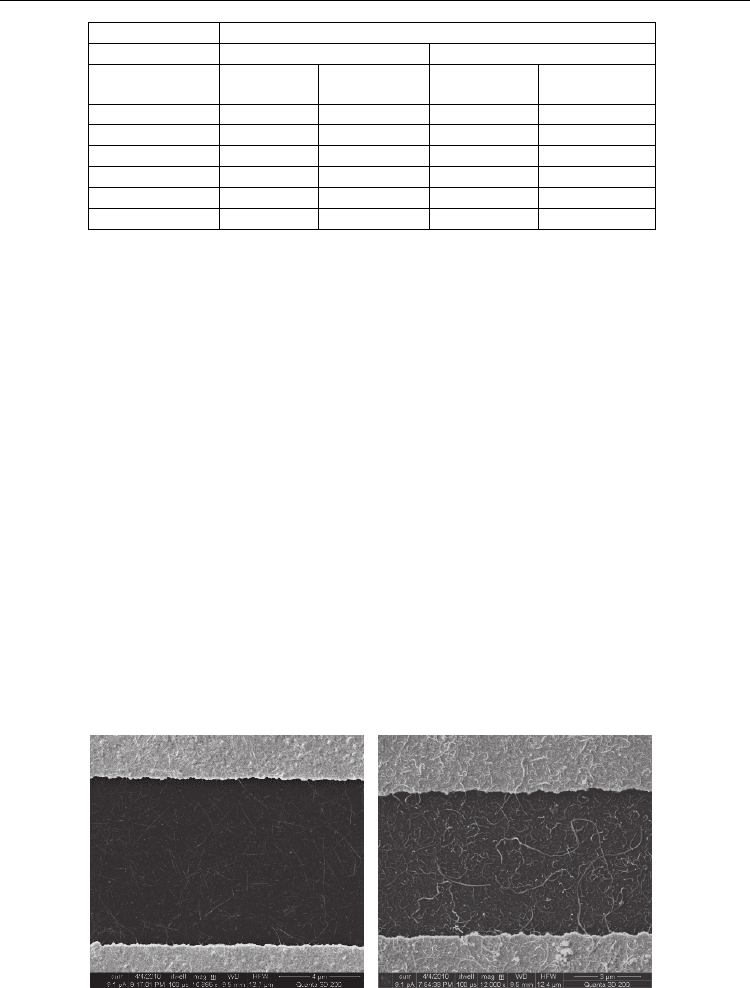
Afterward, the substrate is rinsed with DI water and dried with compressed air. Figure 18
shows the SEM images of random networks for both the SWNTs and the MWNTs. In this
case, the CNTs cover the entire substrate surface including the gap and the electrodes. There
is no CNT alignment observed from these SEM images. Therefore, we can conclude that the
alignment of the CNTs in our investigation is solely caused by the dielectrophoresis process.
Fig. 18. SEM images (a) a SWNT random network and (b) a MWNT random network.
Reprinted with permission from P. Li & Xue, 2010b. @ 2010 American Society of Mechanical
Engineers.
(b)
(a)