Baca A.G., Ashby C.I.H. Fabrication of GaAs Devices
Подождите немного. Документ загружается.

Field effect transistors
of the mesa to the semi-insulating GaAs buffer. The gate metal
should have low reverse leakage currents, which should be con-
trolled by the metal/semiconductor interface of the given epitaxial
structure. However, at the mesa edge, the gate may contact the
InGaAs and be a source of gate leakage current since the InGaAs
has a lower bandgap energy than GaAs. This parasitic gate leakage
is more of an issue for InP substrates, where InGaAs with 49% In
is commonly used, but nevertheless should be characterised for
GaAs PHEMTs or MHEMTs as well. If it is found to be a signi-
ficant source of leakage, the mesa etch can be modified to finish
with a preferential InGaAs etch (Section 4.5.2 and FIGURE 4.11).
Ion implantation is a second method for isolation of FETs.
Doped, conducting layers outside the active FET areas can be
implanted and the resulting lattice damage will make these layers
highly resistive, if the implant is done properly. The proper way of
isolating by ion implantation is to create an optimum concentration
of defect-associated traps with the implantation process. If there
are too few defects, doped areas will exist that can join together
and provide conductive paths. If there are too many defects, elec-
trons can hop from trap to trap under the influence of an electric
field and provide leakage paths. With just the right trap density,
the conductivity of a doped layer can be reduced by 8 orders of
magnitude or more from the peak drain current levels.
One must also take care to design the implant sequence with
the proper projected range and with regard to the total thermal
budget in fabricating the transistor. For example, the other anneal-
ing processes during the fabrication of the FET can reduce the
trap density and lead to suboptimal isolation. Different implant
doses (and optimisation) are required depending on whether the
implant is done before or after the ohmic alloying process (refer
to FIGURES 8.11 and 8.12). A wide variety of ions may be used
to provide isolation by this damage mechanism including O, B, N
and He. Generally, lighter atoms are preferred because they have a
greater projected range at a given energy. Generally, H is not used
because it shows considerable long-term mobility and can diffuse
to regions far from the originally implanted region. It has the poten-
tial to passivate dopant atoms or cause hydrogen poisoning effects
(Section 7.5).
Implant isolation is generally desired before the gate-metal pro-
cess so that the parasitic gate-metal capacitance (that associated
with the gate pad and not the active transistor) is minimised.
However, in a self-aligned process (refer to FIGURE 8.12), an
800–900
◦
C anneal will follow the gate-metal process. Lattice
damage to GaAs from an isolation implant will generally be
repaired at these temperatures. Generally speaking, implant isol-
ation by a purely damage-based mechanism may work up to
252
Field effect transistors
subsequent anneals at 600 to 650
◦
C. An exception is a void
formation process with a very-high-dose Al implantation into
GaAs [5]. Such an implant is stable up to 900
◦
C. However, the
common procedure is to use selective-ion-implantation doping for
self-aligned GaAs MESFETs to avoid a pre-gate isolation step.
One could also use mesa isolation.
For self-aligned HFET structures using AlGaAs-doped layers,
a thermally stable isolation process may be used prior to the
gate process. Oxygen implantation will continue to isolate by the
lattice-damage mechanism when the wafer is annealed at tem-
peratures below 650
◦
C. At higher doses, it will form a chemical
complex with AlGaAs at temperatures of 700–900
◦
C, which will
neutralise the AlGaAs dopants.
Finally, selectively doped FETs may not need isolation if the
resistivity of the substrate is high enough. If the need for an isol-
ation step is eliminated for this reason, it is still necessary to
control surface leakage currents and ensure process compatibility
with subsequent high-temperature steps. In general, it is not easy
to achieve this type of control and may be safer to incorporate an
isolation step as an insurance policy.
8.5 SOURCE AND DRAIN OHMIC CONTACTS
An ideal FET has low channel resistance for high-performance
applications. The resistance (ohmic contact and semiconductor
resistance) associated with the transport of electrons from the
source to the channel adds delay to the FET transit time and is con-
sidered a parasitic effect. It is very desirable to minimise the effect
of ohmic contact resistance on the overall source resistance. Other
important factors for GaAs ohmic contacts are reliability, thermal
stability and shallow and minimally reacting interfaces. These
factors as well as fabrication considerations have been thoroughly
reviewed in Chapter 6.
GeAuNi ohmic contacts have been the mainstay for FET fabric-
ation for more than two decades and nothing on the horizon appears
to threaten that position. Contact resistance of less than 0.1 -mm
is routinely obtained. With today’s high-frequency devices that
have pushed performance above the 200 GHz range for GaAs
PHEMTs (and approaching 400 GHz in InP HEMTs), it would
be desirable to have improvement paths available for ohmic con-
tacts, as well. However, the contact technology is rather mature and
limited in part by peak doping levels achievable in GaAs and sheet
resistance levels achievable in GaAs-based FETs. Unfortunately,
no obvious improvements in electrical characteristics appear to be
on the horizon for GaAs-based contacts.
253
Field effect transistors
The improvements in GaAs contacts over the last several dec-
ades have been in the areas of fundamental understanding of
their reactions and mechanisms, thermal stability and the form-
ation of shallower junctions (refer to Chapter 6 for more details).
PdGe ohmic contacts were developed as an alternative contact for
these reasons and were seriously considered as a replacement for
GeNiAu for enhanced reliability. However, today most FET pro-
cesses, both research and manufacturing, continue to use GeNiAu.
8.6 GATE METAL CONTACTS
As was seen in Sections 8.2.4 and 7.3, a wide variety of gate
metal processes exist for GaAs-based FETs. Processing details
were described in those sections. The choice of gate metal for
an FET depends on the types of process used, the performance
requirements, reliability issues, and manufacturability. All else
being equal, a higher Schottky barrier height is preferred to reduce
gate leakage and forward conduction. As described in Section 7.4,
the Schottky barriers of commonly used contacts to GaAs vary
within a fairly narrow range of approximately 0.2 eV. In spite of
thermally activated reactions of Au with GaAs and the unsatisfact-
ory diffusion barrier properties of Ti and Pt, Au-based contacts
can be reliable against gate sinking (Section 7.5). These types of
contacts raise concerns about hydrogen poisoning, especially for
hermetic packages. Refractory metal contacts are preferred for
self-aligned processes and provide the best diffusion barriers in
low-temperature processes. Some of the best refractory contacts
are WSi
0.45
and WSiN because these remain amorphous for bet-
ter diffusion barrier properties at sufficiently high temperatures to
prevent Ga and As outdiffusion.
8.7 PASSIVATION
The GaAs surface is one of the least understood areas of GaAs
technology, but it remains an area of intense interest and active
research. Moreover, the fundamental understanding that does exist
is based on well-defined starting conditions, which often do not
correlate well with the conditions present on partially-processed
GaAs wafers. The electrical properties of a GaAs FET surface
profoundly affect the device characteristics. The crystal structure
of the surface, defects and chemical impurities can affect the Fermi
level deep in the semiconductor. In addition, these factors can con-
tribute to deleterious surface currents during device operation. For
these reasons, GaAs FET device engineers have sought methods
254
Field effect transistors
of surface passivation that can eliminate or at least stabilise these
effects.
In Section 8.2.4 it was noted that passivation of GaAs FETs
using silicon nitride deposition is sometimes performed as the first
step of processing (FIGURE 8.11) in order to stabilise the surface
in the as-received condition, at which time it is likely to be at
its most reproducible state. Other process engineers have found
ways of controllable processing that can return the GaAs surface
to its most favourable, or at least its most reproducible, condi-
tion at various points in the process, usually by plasma oxidation
treatments followed by oxide removal and native-oxide formation
(Section 6.3.1). A more stable method of passivation is needed
after the active device processing steps. Silicon nitride passivation
was implemented in the 1970s as a “temporary” solution to the
passivation needs of GaAs FETs. It is still in widespread use today!
The first effect of a good passivation is to physically protect the
device from handling and environmental contaminants. SiN
x
is a
good choice for this purpose. While SiO
2
will take up water vapour
and is permeable to mobile ions (even as thermally-oxidisedsingle-
crystal Si), SiN
x
provides a good barrier to both moisture and ions.
It is also a mechanically hard material capable of providing scratch
protection. The SiN
x
film can also have excellent insulating prop-
erties so that it serves well as an insulator between the electrical
contacts.
It is important to protect the GaAs surface against oxidation
(Section 8.8.3), since long-term degradation can occur if GaAs sur-
faces are allowed to oxidise. SiN
x
provides this protection well as
long as no oxygen contamination is present during the deposition.
Sufficiently high purity source gases are available for this purpose.
The trace gases in vacuum systems used for SiN
x
deposition must
be considered potential contaminants as well. Water vapour read-
ily adsorbs on the walls of vacuum chambers that are vented to air
for sample introduction. A loadlocked system will minimise this
source of contamination. Alternatively, the gas-purging proced-
ures as well as the vacuum integrity and operating pressures of the
deposition system must be adequate to minimise contamination
from residual sources of water vapour. The deposition conditions
should be optimised to avoid energetic ions impinging on oxygen-
containing parts (such as anodized Al) within the vacuum chamber
since these may sputter and contaminate the sample.
The SiN
x
film must also be electrically passivating. If this type
of passivation is not performed, the GaAs FET is susceptible
to high levels of RF dispersion and hot electron degradation
(Section 8.8.2). Unfortunately, most of the available art in achiev-
ing electrical passivation is only available in proprietory settings
rather than as publications of careful research studies. If a need
255
Field effect transistors
arises for high-quality SiN
x
passivation, the burden will rest on
the individual process engineer to optimise his or her own process
to arrive at the parameters for depositing a suitable film with the
equipment available. A procedure will be outlined to do this.
First, one must characterise the deposition process and strive
to develop a high-quality baseline film. This involves evaluation
of the refractive index, stress, film composition and the film etch
rate in diluted HF (or buffered-oxide etch, BOE). These proper-
ties can be evaluated by ellipsometry, a stress gauge (based on
laser deflection, usually) and RBS for general composition or
Fourier transform infra-red spectroscopy for hydrogen content.
A low-stress dense film with a low BOE etch rate deposited at a
temperature near 275
◦
C is a good starting point.
Then, one should conduct carefully controlled experiments
where one monitors the drain I-V characteristics on an FET before
and after passivation using a candidate film. One should measure
the DC performance and compare it with the pulsed I-V charac-
teristics. For the pulsed I-V characteristics, one should begin by
biasing the FET with a quiescent bias condition (the bias condi-
tions that are imposed after each pulsed bias condition) of a gate
voltagenear V
th
and a drain voltagenear 5 V. The pulsed conditions
may be adjusted based on what is observed. For each candidate
film, one should compare the pulsed I-V with the DC I-V. Those
films for which the DC I-V most closely matches the pulsed I-V,
especially near the knee, are the best candidate films. Once pas-
sivated FETs with low dispersion (as observed in the pulsed I-V
measurement) are obtained, the FETs are ready to be evaluated for
their intended application.
Another important passivating-film property is the film stress.
GaAs-based FETs are sensitive to the film stress through the piezo-
electric effect. A stress in GaAs will change the electric field in
the GaAs due to this effect. The electric field change is manifested
as a change in V
th
. At the very least, the SiN
x
film should have
a reproducible stress. It is even better for the film to have as little
measurable stress as possible.
8.8 DEGRADATION OF FETS
Like almost everything, FETs can wear out, meaning they degrade
gradually over time, and finally fail in the course of operation.
They can also “burn out”, or fail abruptly. Burn-out failures occur
most often in the initial stages of operation, but not always. In this
section, mechanisms of gradual FET degradation will be the main
topic. The reader should be aware that many of these mechan-
isms also apply to burn-out. Manufacturers of FETs often apply
256
Field effect transistors
“burn-in” stress tests to their entire population of deliverable parts.
This procedure may involve a moderate temperature elevation and
an electrical stress. The purpose of burn-in is twofold: to accelerate
any normal changes in electrical characteristics and to eliminate as
many early failures as possible. The burn-in procedure goes a long
way towards compensating for our often inadequate knowledge
and ability to control all failure mechanisms.
FETs can wear out through interactions (or complications) with
their surrounding environment (the package, for example). We
will ignore these problems for the purpose of this chapter and con-
centrate instead on degradations intrinsic to the FET. Chemical
reactions can degrade the surfaces and interfaces of the FET. These
reactions affect primarily the contacts of the FET (Section 8.5 and
Chapter 7), exposed surfaces, and interfaces with the passivating
film. The reactions can occur at ordinary temperatures over long
periods of time, but they are more likely to be an issue with higher
temperatures and other sources of environmental stress such as
high humidity. The temperature of FETs can rise with the ambi-
ent, but can also rise with the power generated by electrically
operating them.
FETs can also fail due to electrical changes in the semicon-
ductor or its passivating films. Compound semiconductors can
have many defects, most of which are electrically active. Changes
in the charge states of these defects or “traps” can rearrange charge
and cause devices to fail. Even where few defects existed initially,
large electric fields can create new defects in the course of normal
device operation.
It is the responsibility of materials, processing, device and
design engineers, to understand how growth, processing and
device structures affect the electrical operation of devices. The
same applies for how they affect electrical degradation.
8.8.1 Definition and characterisation of hot electrons
The FET is always being engineered to yield higher performance.
For example, higher power, higher gain and higher efficiency
are always desired in power FETs. One approach to achieving
the output power goal is to add gain stages and to add to the
total gate width of the output stage of the final device. However,
this approach has its limits. As the total current increases, the
device impedance becomes extremely small (less than 1 is not
uncommon) and difficult to efficiently match to the load impedance
(50 , commonly). In order to increase power without reducing
the device impedance, higher drain-voltage operation is desired. In
addition, high-performance applications require short gate lengths,
257
Field effect transistors
so peak electric field values can be very high, even for moderate
drain voltages.
Channel electrons of an FET accelerate in an electric field,
alternately gaining energy and losing it in scattering events with
phonons, dopant impurities, defects and other scattering centres.
On average, they gain kinetic energy in proportion to the mag-
nitude of the electric field. For low electric fields (such as in the
source region), the electron population has an average kinetic
energy much lower than the thermal energy of the lattice and
is considered to be in thermal equilibrium with it. As the elec-
tric field increases in the channel region beneath the gate and
on the drain side of the gate, the electron kinetic energy greatly
surpasses the thermal energy and the electrons are said to have
become “hot”. Foran FET with a 0.25 μm gate with its drain biased
at 5 V, the average electric field can approach 2 × 10
5
V/cm; the
peak electric field can be even higher. Such fields are near the
onset of avalanche (multiplication of electron hole pairs due to
energetic electron collisions with atoms in the lattice) breakdown
(4 × 10
5
V/cm) for GaAs.
Hot electrons can exceed the bounds of normal FET operation
in several ways. They may have sufficient energy to escape the
quantum-well confinement of HEMTs, which may have conduc-
tion band offsets in the range of 0.2–0.3 eV, or about 10 times the
thermal energy. In that case, electrons can escape the (In)GaAs
channel into the barrier layer. These electrons can be captured
by deep level traps in the barrier layer, surface states, interface
states of the Schottky gate or the passivation dielectric. Changes
in the charge states of traps can change the threshold voltage of
the device if they occur under the gate or at the Schottky interface.
Although they do not necessarily cause threshold voltage shifts,
they can cause changes in drain current, transconductance, and
other electrical parameters when captured by deep levels in the
drain or drain surface region.
A population of hot electrons reaches a point where a small
but significant fraction possesses energy in excess of the bandgap.
One of these electrons that scatters with the lattice can transfer
enough energy to promote a valence electron to the conduction
band in a process called impact ionisation. The hole that is left
behind contributes to the drain current as it is pulled towards the
source. However, some of the more energetic holes make their
way to the gate, especially if it is biased more negative than
the source. A negative gate current component thus accompanies
impact ionisation. For FETs with low leakage, this source of
gate current is the predominant one at high drain bias and rep-
resents a useful indicator of impact ionisation. An example of
how gate current correlates with impact ionisation is given in
258
Field effect transistors
–0.6 –0.4 –0.2 0.0 0.2 0.4
–1.4
–1.2
–1.0
–0.8
–0.6
–0.4
–0.2
gate current (mA)
gate-source voltage (V)
V
DS
= 6.0 V
V
DS
= 6.5 V
V
DS
= 7.0 V
FIGURE 8.13 The bell-shaped form for gate current of a GaAs FET is a
signature for impact ionisation. (Semicond. Sci. Technol. 13 (1998)
p.1053–63, reprinted with permission.)
FIGURE 8.13 [6]. At drain voltages below 6 V, the gate current
is comfortably below −0.4 mA. For drain voltages between 6 and
7 V, gate currents increase and peak at near −0.2 V. At very negat-
ive gate voltages, the gate current is low because the drain current
is low (the channel is near pinchoff) and few channel electrons are
available to participate in impact ionisation. At high gate voltage,
the gate current also drops; the gate-drain voltage is reduced and
impact ionisation drops dramatically. The bell shaped curve for
gate current is a signature for impact ionisation. In particular, the
I
G
/I
D
ratio is characteristic of impact ionisation and can be meas-
ured non-destructively (at low levels). I
G
is proportional to the
holes generated by impact ionisation and I
D
is proportional to the
number of electrons in the channel.
Of course, impact ionisation can also be observed by a sharp
increase of drain current with drain voltage. There are two prob-
lems with this method of testing. One is that the device is easily
damaged by such a test. The other is that the test is not necessar-
ily definitive for impact ionisation; electron release from traps can
result in a similar increase in the drain current. In the former type of
test, one must make comparisons between several separate devices,
introducing uncertainty since all devices may not be sufficiently
“identical”.
Another useful measure of impact ionisation is by band-to-
band radiative recombination of cold channel electrons (near the
source) with holes generated by impact ionisation. In a unipolar
device such as the FET, impact ionisation is the most likely
259
Field effect transistors
source of holes, so band-to-band electroluminescence is a sensitive
complement to gate current measurements.
The maximum reverse bias that can be applied between the
drain and gate of an FET defines the gate-to-drain breakdown
voltage. It isimportant to distinguish between off-stateandon-state
breakdown [7]. In off-state breakdown, the gate-to-drain voltage
is measured at a low drain current level with V
GS
biased so that
the channel is pinched off. In such a case, the channel current is
low. On-state breakdown is defined as a locus of drain voltages
and drain current pairs that converge to a given drain voltage at a
given gate current.
8.8.2 Hot electron degradation
Hot electrons can considerably stress an FET and lead to degrada-
tion. Virtually any of the characteristics or performance parameters
of a device can be affected. These include gain and power output
in power amplifiers, noise or gain in low-noise amplifiers, and
threshold voltage, drain current and transconductance in either
digital or analogue FETs.
In Section 8.2.3, frequency dispersion and trap-related effects
were introduced. Although these effects can have tangible con-
sequences for high-frequency circuits that are proportional to the
magnitude of the effect, they do not necessarily imply that degrad-
ation is inevitable. For example, power amplifiers with low to
moderate gate lag may or may not be vulnerable to hot elec-
tron degradation under long-term bias stress. In other words, the
initial magnitude of trapping effects is not a predictor of future
degradation. It is, therefore, important to study and understand
the similarities and differences between initial trap-related effects
and those that contribute to hot electron degradation.
Power FETs experience some of the greatest stress from hot
electrons because RF overdrive produces high gate-drain voltages.
The hot electrons may become trapped in states located at the inter-
face between the semiconductor and the passivation layer. They
may also get trapped in the passivation dielectric. The accumula-
tion of negative charge between the gate and drain locally enhances
surface depletion. The most susceptible region in a recessed-gate
FET is the space between the gate edge and the recess edge. In
planar, self-aligned FETs, any part of the surface between the
gate and drain is susceptible. The surface depletion causes an
increase in the drain resistance, and may cause a reduction in
drain current, transconductance, and RF parameters as well. These
effects cause “power slump”, a gradual and permanent reduction
in output power. They may also cause “power drift”, a partially
recoverable form of power slump [8].
260
Field effect transistors
This degradation effect was first discovered in MESFETs as a
result of DC and RF overdrive stress tests. The effect was found to
be greater in HEMTs and PHEMTs. The cause is due to electron
capture in the gate-drain access region. Thedrain-current reduction
and drain resistance (R
D
) increase was found to be proportional to
the impact ionisation rate, i.e. the I
G
/I
D
ratio [9]. Newly created
traps or deep levels of varying activation energies accompany the
degradation [10].
Significant V
th
shifts during hot electron stress of HEMTs have
also been observed by manygroups. The shifts may often be revers-
ible, at least partially. In many cases, it has been postulated that
negatively charged traps exist in the AlGaAs layer under the gate
and holes created by impact ionisation can be captured by these
traps to neutralise the negative charge. Such an effect causes a
negative shift in V
th
, since positive charge accumulated under the
gate favours electron accumulation in the channel. Similar negat-
ive V
th
shifts have been observed in high-temperature storage tests
of some commercial PHEMTs at temperatures of 120
◦
C to 240
◦
C,
indicating that thermal detrapping of electrons in the AlGaAs may
be responsible. This thermally activated process has an activa-
tion energy of 0.21 eV and is reversible in tens of hours at room
temperature [11]. In cases where the V
th
shift is permanent, posit-
ive charge may be stored in the thin interfacial layer between the
Schottky metal and the HEMT barrier layer.
Some cases of permanent positive V
th
have been observed after
hot electron stress. Formation of deep levels (1.2 eV activation
energy) under the gate or on the drain side of the gate have been
postulated [10]. Competing effects are possible as well.
A curious effect happens with hot electron stress with respect
to breakdown. Most new traps created by the stress either degrade
performance or cause large enough changes over a long enough
time that a burn-in to stabilise them is not a viable option. How-
ever, a slight increase in the number of traps created during initial
operation of an FET may increase its breakdown voltage without
significantly changing other FET parameters. To achieve this, an
FET is stressed with an appropriate impact ionisation current (kept
constant during the stress) and the drain voltage is observed to
rise gradually, resulting in “breakdown walkout”. This effect may
happen in seconds or minutes and the extent of the breakdown
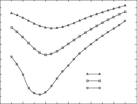
walkout is often several volts, as illustrated in FIGURE 8.14.
The effect was first discovered for unpassivated AlGaAs/GaAs
HEMTs [12], where it was attributed to oxidation of the exposed
AlGaAs. The effect was much smaller for passivated HEMTs and
MESFETs. Commercially-passivated PHEMTs are also suscept-
ible, and negative charge at the surface of the drain access region
is thought to be responsible [13]. The latter effect is clearly related
261