Baca A.G., Ashby C.I.H. Fabrication of GaAs Devices
Подождите немного. Документ загружается.


Field effect transistors
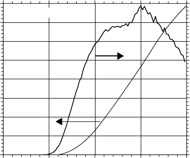
most positive (usually defined by the onset of gate current and
corresponding to the highest drain currents). The gate voltage is
stepped negative until pinchoff is reached. For a given gate voltage,
the drain current increases initially with increasing drain voltage,
reaches saturation at the drain voltage that defines the knee (the
transition from linear to saturation currents) and is fairly steady for
larger drain voltages. In the region of linear increase, the applied
drain voltage leads to higher drain current through the following
relation:
I
D
= qμV
D
(8.2)
SGD
V
D
=0
(a)
SGD
V
D
<V
knee
(b)
SGD
V
D
>V
knee
(c)
FIGURE 8.3 Depletion region of
a gate at fixed gate bias and under
various drain biases.
where q is the electron charge and μ is the electron mobility.
As the drain bias is increased, electrons travel across the gate
region with higher velocity. The gate depletion region is altered
by the presence of the gate voltage, as illustrated in FIGURE 8.3.
FIGURE 8.3(a) illustrates a gate depletion region for a transistor
with no drain bias, while FIGURES 8.3(b) and 8.3(c) illustrate
an FET with a drain bias below the knee voltage and above the
knee voltage, respectively. The drain end of the gate experiences
a more negative potential as a result of the drain bias, which
results in a larger depletion region. The knee voltage results in
pinchoff at the drain end of the gate. At this bias, the rest of the
gate is screened from further drain bias increase and does not
modulate significantly with higher drain voltages. Although the
channel is pinched off in a small region along the drain side of
the gate in this simple model, two-dimensional calculations show
that a small undepleted channel exists, accounting for the non-
zero current flow. Higher drain bias does not further deplete the
channel and the current saturates. The depletion region can con-
tinue to extend towards the drain with further drain bias increase.
This effect is considered in designing the crystal growth and in
choosing processing steps in terms of how the gate edge region
is doped in epitaxially-grown structures or self-aligned structures.
This model of MESFET action is the Shockley model and gener-
ally describes long-channel devices [4]. In short-channel devices,
velocity saturation also plays an important role.
Apart from knee-voltage determination, the drain I-V character-
istics give other insights into the FET. Ideally, the drain current in
the saturation region is flat. In short-channel devices, the drain cur-
rent may increase with drain bias and special designs are employed
to minimise this. In large-periphery devices, a decrease in drain
current with drain voltage could be a thermal effect due to self-
heating; this can be managed with proper diagnosis. Finally, kinks
in the drain current as a function of drain bias can be an indication
of surface or trap-related anomalies that affect performance or
reliability.
232
Field effect transistors
0
50
100
150
200
250
300
350
400
0
50
100
150
200
250
300
350
400
0.4 × 40 μm
2
–0.5 0 0.5 1 1.5
drain current (mA/mm)
transconductance (mS/mm)
gate bias (V)
drain bias: 1.5 V
FIGURE 8.4 Plot of drain current and transconductance versus gate voltage.
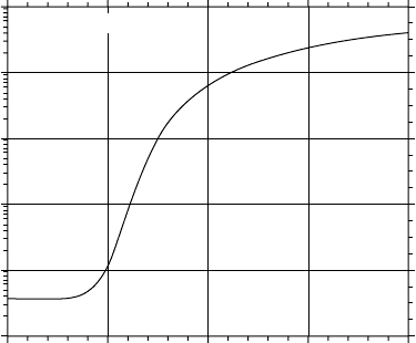
Another common DC measurement is illustrated in FIGURE 8.4.
The drain current is plotted against the gate voltage. The slope of
the drain current gives the transconductance, g
m
, of the device.
High transconductance is important as it is directly related to the
speed of the device by the relation
f
t
= g
m
/2πC
gs
(8.3)
where f
t
is known as the cutoff frequency (described shortly)
and C
gs
is the gate-to-source capacitance. High transconductance
also helps to increase the power density and maximum power
output of a microwave amplifier. It can also minimise the tran-
sistor size required to switch a given current in a high speed
digital circuit. The I
D
–V
G
plot is also the most useful way to
determine the threshold voltage of an FET and to examine the
subthreshold current characteristics. Sub-threshold current ana-
lysis is most useful if it is viewed as a log plot, as in FIGURE 8.5.
One strives to maximise the logarithmic slope and minimise the
lowest current level.
The measurements of FIGURES 8.2 and 8.4 have been
described here as DC measurements, but they may also be
made with short-current pulses (as short as 100 ns) to distinguish
between thermal and trapping effects. Trapping effects play a large
role in many aspects of FET performance and degradation, as will
be described in Sections 8.2.3 and 8.8. Pulsed I-V measurements
are critical in analysing these effects.
GaAs FETs are most commonly used in high-performance
applications, such as amplifiers that involve high frequency, low
233
Field effect transistors
0.4 × 40 μm
2
–0.5 0 0.5 1 1.5
drain current (mA/mm)
gate bias (V)
0.01
0.1
1
10
100
1000
drain bias: 1.5 V
FIGURE 8.5 Logarithmic plot of drain current versus gate voltage.
noise or power with high linearity. For devices and circuits,
time-dependent current-voltage characterisation is sufficient to
completely describe a circuit. This method of characterisation
works well if the frequency is low enough that the device (circuit)
dimensions are small compared to the wavelength (the inverse
frequency) at the frequency of interest. At microwave frequen-
cies (λ = 1 cm at 30 GHz), this assumption breaks down and it
becomes impossible to get accurate time-dependent I-V data. The
high-frequency performance is usually characterised with scatter-
ing parameter (S-parameter) testing. An S-parameter test is one
where the intensity of scattered and reflected waves for an incid-
ent (usually high-frequency) signal is measured at each port for
an arbitrary n-port network. The FET is represented as a 2-port
network for this type of characterisation, with ports at the gate and
drain. The S-parameters can be converted to several other domains,
where they can be related to voltages and currents in the device.
The HBT (Chapter 9) is characterised with ports on the base and
collector. For more details on high-frequency characterisation, the
reader is referred to [1].
Equations are readily available to transform S-parameter data
to other forms that allow one to derive high-frequency para-
meters of interest. The y-parameters transform the currents in
a device to voltages. The z-parameters transform voltages in a
device to currents and h-(hybrid) parameters perform a mixed
(current, voltage) transformation. When this transformation is
carried out for S-parameters to h-parameters, h21 describes the
current gain of a device. When plotted as a function of frequency
as in FIGURE 8.6, its extrapolation to unity current gain defines
234

Field effect transistors
Msg
H
21
Mag
f
max
= 160 GHz
f
t
= 120 GHz
0.1 1 10 100 1000
0
10
20
30
40
50
power and current gain (dB)
frequenc
y
(GHz)
Mag@50 GHz = 9.2 dB
FIGURE 8.6 Example plots used to extract f
t
and f
max
in a FET. (IEEE
Microwave and Guided Wave Lett. vol.9 (1999) p.28–30, reprinted with
permission.)
the f
t
of a device. The f
max
is defined as the extrapolation to unity
of the unilateral power gain, U, or alternatively as the maximum
stable gain. Likewise, equations are readily available to trans-
form S-parameter data to U. Extrapolation to unity gain is done
using a 20 dB/decade slope, rather than a direct extrapolation of
data as seen in FIGURE 8.6. Many device researchers focus on
high-frequency measurements such as f
t
and f
max
, but other high-
frequency measurements such as amplifier gain and noise figure
are important as well.
FETs are often electrically described as a circuit in order to write
equations that describe their physical or electrical behaviour. Such
a description is termed an “equivalent circuit” and is used to predict
the behaviour of circuits built from FETs. An example of an equi-
valent circuit description of an FET is shown in FIGURE 8.7. In
this example, some of the equivalent circuit elements have an obvi-
ous correlation to a physical part of the transistor. For example, the
source and drain ohmic contacts are represented by the resistors,
R
S
and R
D
. However, in other cases, no direct physical correlation
is made. Equivalent circuits used for the prediction of circuit oper-
ation should accurately model the transistor with a minimum of
components so that circuits with high complexity can have man-
ageable computational requirements. On the other hand equivalent
circuits whose intent is to accurately model the physics of the FET
often tend towards more complex models with as many physic-
ally based parameters as is practical. Equivalent circuit models
for FETs are usually built from a combination of DC, pulsed and
S-parameter measurements.
235

Field effect transistors
SGD
Ld
Ls
Rs Rd
Cb
Ce
Cb
Cpd
p-GaAs
semi-insulating GaAs
n+ GaAs
n GaAd
Rg
Lg
Cpg
FIGURE 8.7 Example of an equivalent circuit description of an FET. (IEEE
Trans. Microwave Theory Tech. vol.49 (2001) p.1410–18, reprinted with
permission.)
8.2.2 Field effect transistor performance and
reliability issues
FETs have performance and reliability issues that are often inter-
related and so are presented here in the same section. Ideally,
FET dimensions and materials properties would determine per-
formance limits. Dimensions would systematically be reduced
through improvements in processing equipment. Even using litho-
graphy tools two to three generations behind the Si world, GaAs
technologies compete with current Si devices in certain meas-
ures of performance such as linearity and power-added efficiency.
Materials choices impact performance and reliability through their
inherent physical properties and complex interactions. Materials
scientists have been engineering GaAs-based materials for several
decades now, and much has been learned.
Thermal effects are extremely important considerations for
high-performance FETs. The performance of an FET generally
reaches its highest level at biases that give the highest transcon-
ductance (refer to FIGURE 8.4). The power dissipation of the
transistor (voltage-current product) leads to heat flow away from
the transistor as well as self-heating of the device. Accordingly, a
given current level will lead to greater self-heating at higher drain
bias. This is seen in the I-V characteristics when they are taken
to higher drain bias, as in the slight droop of the top curve near
236
Field effect transistors
7.0 V in FIGURE 8.2. The performance of an FET as measured by
f
t
and f
max
will generally decline as a function of drain bias due
to self-heating effects. The peak in f
t
is often near a drain bias of
1.0 V for GaAs FETs.
Note: The term junction temperature
comes from HBT terminology and is
widely used by FET engineers as well.
Strictly speaking, “channel” or
“Schottky” temperature would be more
accurate descriptions of FETs.
Not surprisingly, FET degradation is accelerated by temperature
and is impacted by the self-heating effects that lead to an increase
in the junction temperature of an FET. Calculation of the junction
temperature depends on howthepower is thermally dissipated. The
following equation describes the relation between the temperature
rise and the dissipated power for an FET in thermal contact with a
perfect heat sink, i.e. one that does not experience a temperature
rise in response to a thermal load:
T = R
th
I
D
V
DS
(8.4)
T is the junction-temperature rise over the heatsink temperature,
R
th
is the thermal resistance of the semiconductor and I
DS
and V
DS
are the drain current and drain voltage. The thermal resistance R
th
is dependent on the geometry and the thermal conductivities of the
materials in contact with the FET.
GaAs is a poor thermal conductor compared to Si (by a
factor of three) and to some of the metals commonly used as
interconnects, packaging materials and heatsinks. Junction tem-
peratures for GaAs FET power amplifiers can commonly attain
and even exceed 150
◦
C, although smaller devices in other types
of analogue and digital circuits can operate at lower temperat-
ures. High junction temperatures have important implications for
device, processing and reliability engineers. First, electron trans-
port degrades with increasing temperature. The thermal energy of
common lattice vibrations (phonons) increases with temperature
and causes more electron scattering. Both electron mobility and
saturated velocity decrease with increasing temperature. These
factors negatively affect the transit time of FETs and therefore
their high-frequency performance.
As an example of the potential for thermal effects to affect
performance, consider a high-linearity FET power amplifier. The
output power at a given frequency needs to be linearly proportional
to the input power and meets this requirement at low input levels.
At high enough input levels, the dissipated power of the device
causes significant self-heating, which in turn degrades electron
transport. The gain of the device drops and the output power is no
longer linearly related to the input. Unless the heat can be managed
better to control the junction temperature, the linear output power
limit will have been reached.
High junction temperatures also have the potential to accelerate
the aging of some of the materials of the FET. As discussed in
237

Field effect transistors
Chapter 6, reactions of GaAs with Au, Ni and other ohmic contact
constituents occur within minutes and sometimes within seconds at
temperatures of 300
◦
C and above. It is not unrealistic to expect that
some of these reactions can occur at temperatures of 150–200
◦
C
after a sufficient time. The same is true for thermal acceleration of
the metallurgical reactions of some Schottky contacts.
Thermal-management solutions are sought to keep device tem-
peratures below this upper junction temperature limit. Some
common techniques in practice are the thinning of the GaAs sub-
strate, sometimes to as thin as 50 μm, and judicious spreading of
the gate fingers.
Another important performance issue relates to discrepancies
found between low- and high-frequency measurements. Well-
optimised devices perform in good agreement with physically-
based models that set performance expectations for material
parameters such as saturated velocity and mobility. These para-
meters are related through well-understood physical derivations
to the current, transconductance and transit time in an FET. How-
ever, devices often show deviation from expected values of some
of these parameters at high frequencies, an effect known as fre-
quency dispersion. Output conductance (the slope of the drain I-V
curve in the saturation region) and transconductance of all GaAs
FETs show frequency dispersion to some degree. Those FETs
and their processes or materials that display low degrees of fre-
quency dispersion have obvious advantages for the companies that
sell them.
gate voltage
drain current
time (ms)
DC current
FIGURE 8.8 The current in an
FET may not follow the voltage
pulse on a fast timescale. This
effect is known as “gate lag”.
A performance issue probably related to frequency dispersion
is known as “gate lag”, which is illustrated in FIGURE 8.8. An
arbitrary combination of gate voltage and drain voltage will imply
a given drain current according to an FET’s expected characterist-
ics, such as those illustrated in FIGURE 8.2. However, when such
voltages are applied to an FET with a fast pulser and viewed on a
fast oscilloscope, the current response does not reach the expected
DC current on a timescale that is very fast compared with the elec-
tron velocity. For example, an FET that is biased in the “off ” state
receives a fast pulse to the gate biasing the FET to the “on” state.
A fraction of the expected DC current is measured on a short times-
cale (1 μs, for example), while the remainder of the current takes a
much longer time (milliseconds, for example) to appear. The time
lag in recovering to the expected DC current level is called “gate
lag” if the gate is pulsed and “drain lag” if the drain is pulsed.
Electron traps are acknowledged to be responsible for many of
these transient effects. Recall that a trap is a midgap state that is not
mobile. Free electrons will respond rapidly to a change in electric
field and the free-electron currents will adjust on a timescale of
the order of the transit time of an electron (picoseconds). However,
238
Field effect transistors
the traps will respond to the new conditions with much slower time
constants because of the need to overcome an activation energy
for the carrier to “de-trap” and become mobile. Also, fixed charge
associated with the traps creates depletion regions that reduce the
number of mobile carriers.
We shall now describe a few ways that traps negatively affect
device performance and applications. Specific FET manifestations
of some trapping effects will be discussed in Section 8.8. The crux
of the problem is that both analogue and digital circuits can have
rapid changes in bias conditions that can trap electrons during one
part of their operating cycle and slowly release them in another
part of the cycle. If large enough in magnitude, the effects can
lead to unpredictable logic errors in digital circuits. In a microwave
amplifier with drive conditions large enough to fill trap states in
part of the cycle, the circuit operates under a continual state of
trapped charge with the RF currents, and therefore power, sig-
nificantly lower than those implied by DC measurements. Many
high-performance metrics scale directly with the extent of fre-
quency dispersion, and gate lag can be a useful screening test for
bias conditions relevant to the application.
Many of these trap-related effects can be reduced or exacerbated
by common process choices and must be considered by process
engineers. Gate geometries and passivation are examples of these
process choices and are described in Sections 7.3 and 8.7. The
trap-related performance issues become degradationandreliability
issues (Section 8.8) when long-term operation can cause perman-
ent changes in the trapping effects and lead to a performance
decline.
One big factor in FET performance is parasitic capacitance
between device elements and the substrate. These effects are
minimal in semi-insulating GaAs and other compound semi-
conductors, but are an important factor in Si-based technology.
A semi-insulating substrate is needed for low-loss microwave
integrated circuits on GaAs and reduced parasitics in high-speed
digital circuits. The differences between GaAs and Si substrates
are a result of both the physical properties and the crystal growth.
GaAs has a higher bandgap than Si and consequently has a lower
intrinsic carrier concentration. Both Si and GaAs can incorpor-
ate impurities at a parts-per-billion level that dope the material
and can lead to uncontrolled substrate resistivity and doping
type. Si technology deals with this by using substrates with
controlled doping and by constructing pn junctions for back-
side isolation from the substrate. GaAs technology deals with
the background doping issue by incorporating deep levels in the
crystal growth to compensate the background doping. The most
common deep level in GaAs is a crystal defect known as EL2,
239
Field effect transistors
which is incorporated in concentrations near 10
16
cm
−3
and can
vary over an order of magnitude depending on the crystal growth
method.
Non-ideal scaling of FETs also affects performance. Ideally,
device geometry is optimised for an FET and increases in per-
formance occur stepwise in succeeding generations of process
technology through proportionally reducing all of the key equi-
valent circuit values (mostly resistances and capacitances) that
affect FET performance. Scaling the FET in this manner usually
requires a proportional reduction in all device dimensions and
generally requires increases in effective doping or charge dens-
ity. Strictly proportionate scaling of GaAs FETs is no longer
possible because many of the material, processing and physical
limits are being approached, especially for the vertical dimensions
(e.g. channel thickness) and dopant concentrations. Consequently,
generational performance increases now require complex tradeoffs
between device design and processing. Non-ideal effects arise
from shortening the gate length of the device without proportion-
ally reducing all equivalent circuit parameters; these are termed
“short-channel” effects. Improved processing strategies are needed
to address short-channel effects.
Much more can be written about performance, especially in
the context of specific applications that may involve circuit speed,
noise performance, power-added efficiency and linearity. Some of
these topics are specifically addressed in sections where process
choices affect them. Others are not addressed in this book.
8.2.3 Field effect transistor structures and materials
Two basic types of transistors are made with GaAs materials: het-
erostructure field effect transistors (HFETs) and metal-
semiconductor field effect transistors (MESFETs). MESFETs
utilise a Schottky contact for the gate and the semiconductor
portion of the device is entirely GaAs. Heterostructure FETs
contain one or more heterojunctions in the material structure,
as in AlGaAs/GaAs high-mobility electron transistors (HEMT),
for example. A HEMT is a special case of an HFET, where the
donor ions reside in a high-bandgap layer (most often AlGaAs or
InGaP) and the mobile carriers reside in the adjacent low-bandgap
layer (most often GaAs or InGaAs), as illustrated in FIGURE 8.9.
Often the low-bandgap material is also doped or other adjustments
are made to the classic HEMT structure, and these devices are
generally referred to as HFETs.
The classification of FET structures can be more complex, but
we will generally refer to two basic types: recessed-gate struc-
tures and planar structures. The geometries, types of structures
240
Field effect transistors
2DEG
E
C
E
F
E
V
FIGURE 8.9 Illustration of the conduction and valence bands of a
two-dimensional electron gas used in HEMTs.
and common methods of processing these gates are presented in
Chapter 7.
Typical HEMT and MESFET structures are illustrated in
FIGURE 8.10. The active layers tend to be very thin, which places
constraints on the manufacturing method for forming the struc-
ture. Ion implantation has historically been the most cost-effective
method of forming the doped regions for GaAs MESFETs
(FIGURE 8.10(a)) and has contributed to their entry in high-
volume commercial markets. However, ion-implantation doping is
a less precise method for forming doped regions of FETs and is less
applicable to very thin active layers for high-performance devices.
Historically, epitaxy has been used for high-performance specialty
markets (military, test equipment) and ion implantation for high-
volume commercial markets. In recent years, the production of
epitaxial substrates has become much more cost-effective and the
performance/cost tradeoff balance has tilted in favour of epitaxial
substrates even in many commercial markets.
n-GaAs channel
n
+
cap
S
G
D
undoped-GaAs buffer and substrate
(a)
30–100 nm
30–200 nm
n-AlGaAs barrier
n
+
GaAs cap
S
G
D
(b)
30–50 nm
25–40 nm
δ-doped layer
undoped AlGaAs spacer
2-dimensional electron gas
undoped-GaAs buffer and substrate
2–5 nm
FIGURE 8.10 Illustration of
typical structures for (a) MESFETs
and (b) HEMTs.
Several types of HEMTs (FIGURE 8.10(b)) are in commercial
use and many variations are subjects of continuing research. In
the pseudomorphic HEMT (PHEMT) structure, a strained InGaAs
layer is inserted between the AlGaAs/GaAs channel interface of
FIGURE 8.10(b). The InGaAs alloy has better transport proper-
ties (higher mobility and saturated velocity) than GaAs, which
lead to higher f
t
and f
max
, and better noise properties. Strained
InGaAs will relax by forming misfit dislocations and render the
PHEMT unusable if the In mole fraction or the total thickness
exceed a critical value. InGaAs with 20% In and 15 nm thickness
is commonly used. PHEMTs were initially developed for military
and space applications due to the higher cost of MBE epitaxy
in the early 1990s. They have since become prevalent in con-
sumer applications due to cost reductions in the epitaxy, now that
high-throughput MBE and MOCVD technologies have matured.
241