Baca A.G., Ashby C.I.H. Fabrication of GaAs Devices
Подождите немного. Документ загружается.


Field effect transistors
0 1 2 3 4 5 6 7 8 9
0
10
20
30
40
50
60
70
80
V
DS
(V)
I
DS
(mA)
after stress
before stress
FIGURE 8.14 The breakdown voltage of a GaAs FET will “walk out” with
drain bias stress during its initial operation. (IEEE Trans. Electron Devices
vol.43, (1996) p.543 reprinted with permission.)
to hot electrons and is clearly not a degradation because it does not
significantly change other FET parameters. Although not a degrad-
ation, breakdown walkout is included in this section because of
similarities to the mechanisms of hot electron degradation.
This effect has a certain elegance to it. Device designers strive
mightily to reduce peak electric fields in a device in order to max-
imise breakdown voltage. Yet, if they don’t completely succeed,
hot electrons naturally find these regions, are drawn to them, and
create the negative surface charge that moderates the peak electric
field. Slight moderation of the peak electric field need not cause
degradation of other device parameters, but once the walkout effect
is completed, hot electron stress should be reduced in order to
reduce any ensuing gradual degradation.
In Section 8.2.2, short timescale, reversible trapping effects
were described. These trapping effects manifest themselves on
a timescale of sub-microseconds to hundreds of milliseconds.
Pulsed I-V measurements (either gate or drain is pulsed) are a
powerful tool for characterising these effects. Transient effects
involving gate pulsing are known as “gate lag” and those involving
drain pulsing are known as “drain lag”. Because of the obvious
similarity with degradation effects discussed in this section and the
potential for confusion, we shall briefly contrast these effects in a
waythat emphasises generalised rather than complete descriptions.
In gate lag, traps are populated with negativegate biases, usually
near but more negative than pinchoff. A lesser dependence on drain
voltage exists. Traps may have various physical locations, but in
262
Field effect transistors
well-optimised materials, the FET surface near the drain edge is
the most susceptible. In such cases, the effect of gate lag will be to
modulate the drain resistance of the device (and properties related
to it, such as the drain current and transconductance). In other
cases, the gate lag affects traps under the gate and changes the
threshold voltage of the device. Most often, gate lag is correlated
with the processing and geometry of the gate, although material
growth conditions can also have an effect. Gate structure design
and surface-passivation solutions to gate lag have been reported.
Generally, recessed-gate structures are less susceptible than
planar structures and shorter gate-edge-to-recess-edge distances
have lesser gate lag than longer ones. Structural designs that place
the physical locations of surface traps in regions of lower peak
electric fields are an effective strategy. Surface-passivation effects
are less well understood. Many new approaches to surface passiv-
ation are described in Chapter 3 and new understanding of how
to manipulate surface properties is gained every year. To date,
none of these fundamental approaches to surface passivation has
replaced the oldest method using amorphous, partially hydrogen-
ated silicon nitride (Section 8.7). This “temporary” fix to transient
surface effects has been with us for more than two decades and a
basic understanding of the origin of its effectiveness is still lack-
ing. Somehow the surface trap energetics are modified by the
SiN
x
/(Al)GaAs interface so that negatively charged traps either
are not energetically favourable, can de-trap on a fast timescale or
can conduct the charge away through slight surface or interface
conduction.
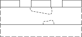
SGD
FIGURE 8.15 In “drain lag”
traps are populated (or
depopulated) by high drain bias.
These traps can cause depletion
changes at the back of the channel
leading to V
th
shifts.
In drain lag, traps in the substrate can be affected by changes in
the drain bias of the FET. These traps can deplete the channel from
the backside, as illustrated in FIGURE 8.15. As in gate lag, rapid
changes in drain bias do not allow sufficient time for the traps to
respond. One will generally observe a threshold voltage shift as
the main effect due to drain lag. Drain lag effects can be more
indicative of growth defects, or other types of substrate defects,
than of process conditions.
Gate and drain lag exist in an FET because of traps that are cre-
ated by the wayit is grownor processed. Although low gate or drain
lag is desirable for performance reasons, FETs with gate or drain
lag can be stable in operation, and therefore reliable. By contrast,
degradation of an FET can occur because of traps or other fixed
charge centres that are usually created by hot electron stress after
growth and processing. The susceptibility to such trap creation
may be affected by growth or process conditions. Hot-electron
stress tests are important to determine safe operating limits, to
prevent degradation and to use as feedback for optimising device
structures, growth and process conditions.
263

Field effect transistors
Although gate lag need not lead to degradation, a screening test
based on gate lag is possible. Reversible gate lag will exist to a
small degree in even the best devices. However, in some devices
that were later shown to degrade, early changes in the magnitude
of the gate lag were observed as well, while other devices that did
not degrade showed stable gate lag [8].
From the preceding discussion, it is clear that the properties of
SiN
x
are critical to the electrical as well as the physical passivation
of GaAs FETs. Little is actually known about its electrical proper-
ties, except that many interface states exist when MIS diodes are
fabricated using SiN
x
as the MIS dielectric. Section 3.3.5 contains
a discussion of MIS diodes and interface states.
A wide variety of possible explanations for the effectiveness
of SiN
x
exist. SiN
x
could play a role in rapidly detrapping deep
levels by providing a conductive path along the SiN
x
/GaAs inter-
face. A Si-rich film could play a role in the interface conductivity.
SiN
x
could also modify the traps through interface reconstructions.
The modified traps could then cease to trap mobile charges under
the conditions of FET operation or could change their time con-
stants for de-trapping such that slow transient effects in the FET
are no longer possible. Whatever the cause, no detailed physical
explanation has yet been conclusively verified.
8.8.3 Other types of degradation
The main other source of degradation is due to oxidation of the
GaAs. One main purpose for SiN
x
passivation is to act as an imper-
meable film to protect the GaAs device from environmental sources
of contamination. When this protection is not in place, the GaAs
surface can oxidise according to the following reactions:
2GaAs + 3O
2
= Ga
2
O
3
+ As
2
O
3
(8.5)
2GaAs + As
2
O
3
= Ga
2
O
3
+ 2As (8.6)
These reactions, described in greater detail in Section 10.2, create
free As at the GaAs/SiN
x
interface and change the interface state
properties. As was described in Sections 8.8.1 and 8.8.2, the
GaAs/SiN
x
interface in the gate-to-drain region of the FET is espe-
cially sensitive to its electrical properties. As seen in Sections 8.3
and 8.7, one goes to great lengths to create high-quality GaAs sur-
faces prior to critical process steps such as dielectric passivation
in order to promote stability and reproducibility in the FET.
As As
depletion
region
oxide
GaAs
FIGURE 8.16 Continued
oxidation of GaAs can lead to As
precipitates in addition to free
surface As. The precipitates act as
local centres for depletion regions.
Arsenic is problematic both as isolated atoms and as precipitates.
While As atoms create undesirable midgap states, the condensa-
tion of atoms into multiatomic precipitates produces many tiny
depletion regions centred on the precipitates (FIGURE 8.16).
264
Field effect transistors
This phenomenon is the origin of the insulating character of
thermally annealed low-temperature-grown GaAs, which is delib-
erately grown rich in As to enable formation of As precipitates
upon annealing. Continuing production of As due to long-term
slow oxidation of the GaAs surface may lead to the formation
of local Schottky barriers and the formation of a non-uniform
potential distribution at the interface.
For this type of degradation to occur, the FET passivation must
be permeable to sources of oxygen (i.e. SiO
2
) or contaminated
with oxygen. High-density SiN
x
films are generally impermeable
to oxygen and water vapour but do incorporate oxygen in the films
fairly easily at levels of a few percent. Whether the oxygen is
securely immobilised in covalent bonds or available to oxidise the
GaAs surface is open to question. However, it is entirely plausible
that energetic electrons can gradually free up oxygen to oxid-
ise the GaAs surface, which will lead to gradual degradation of
the FET. For this reason, most manufacturers of GaAs devices
strive to produce oxygen-free SiN
x
films.
8.9 CONCLUSION
The FET is greatly affected by the surface and interface proper-
ties of GaAs and its contacts. These process-sensitive elements
of the FET need to be understood and controlled by process
development engineers. FET operation, testing and performance
characterisation supply the basic information that materials, pro-
cessing and device engineers need to understand the often complex
materials and process interactions. Many FET process choices
are available and some of the main ones have been reviewed in
this chapter. High-quality contact choices are readily available for
GaAs FETs, as long as one considers the thermal stability and
hydrogen poisoning issues. Minefields must be navigated care-
fully for certain device and process design issues. Peak electric
fields must be suppressed to the extent possible in order to provide
adequate breakdown voltage and reliability consistent with per-
formance requirements. One approach to achieving this end is
to optimise the geometry of a recessed-gate process or the LDD
implants for a self-aligned process. Finally, a high-quality SiN
x
passivation process must be developed and implemented in the
present absence of perfect understanding.
REFERENCES
[1] W. Lui [Fundamentals of III-V Devices: HBTs, MESFETs, and
HFETs/HEMTs (John Wiley and Sons, New York, 1999)]
[2] M. Shur [GaAs Devices and Circuits (Plenum Press, New York, 1987)]
265
Field effect transistors
[3] S.M. Sze (Ed.) [High-Speed Semiconductor Devices (John Wiley and
Sons, New York, 1990)]
[4] A.S. Grove [Physics and Technology of Semiconductor Devices (John
Wiley and Sons, New York, 1967)]
[5] K.-Y. Ko, S. Chen, S.-T. Lee, G. Braunstein [Appl. Phys. Lett. (USA)
vol.60 (1992) p.1223]
[6] R. Menozzi [Semicond. Sci. Technol. (UK) vol.13 (1998) p.1053]
[7] J.A. Del Alamo, M.H. Somerville [IEEE J. Solid-State Circuits (USA)
vol.34 (1999) p.1204]
[8] J.C.M. Hwang [Solid-State Electron. (UK) vol.43 (1999) p.1325]
[9] G. Meneghesso, A. Paccagnella, Y. Hadab, C. Canali, E. Zanoni [Appl.
Phys. Lett. (USA) vol.69 (1996) p.1411]
[10] R. Menozzi [Semicond. Sci. Technol. (UK) vol. 13 (1998) p.1053]
[11] G. Meneghesso, C. Canali, P. Cova, E. De Bortoli, E. Zanoni [IEEE
Electron Device Lett. (USA) vol.17 (1996) p.232]
[12] P.C. Chao, M. Shur, M.Y. Kao, B.R. Lee [IEEE Trans. Electron Devices
(USA) vol.39 (1992) p.738]
[13] R. Menozzi, P. Cova, C. Canali, F. Fantini [IEEE Trans. Electron Devices
(USA) vol.43 (1996) p.543]
266
Chapter 9
Heterojunction bipolar transistors
Chapter scope p.267
HBT basics p.267
Bipolar transistor tutorial p.268
Other GaAs HBT performance and
reliability issues p.272
HBT device structure and material
issues p.275
Overview of HBT fabrication p.279
MESA etching for GaAs-based
HBTs p.281
Emitter mesa etch p.281
Base mesa etch p.285
Collector mesa etch p.286
Ohmic contacts for GaAs-based
HBTs p.286
Emitter metal ohmic contacts p.286
Base metal ohmic contacts p.287
Collector metal ohmic contacts p.289
Passivation of GaAs-based
HBTs p.289
Ledge passivation p.290
Dielectric passivation p.291
Sulphur passivation p.294
Variations on HBT processing p.294
Reliability of HBTs p.299
Conclusions p.303
References p.303
9.1 CHAPTER SCOPE
This chapter will cover most of the basic active processing steps in
GaAs heterojunction bipolar transistors. The active steps are those
that are related to processing the GaAs and whose nuances require
an understanding of the GaAs semiconductor surface and its inter-
face to metal junctions for etching and contact formation. HBTs
present many active processing subtleties with important implic-
ations for device design and operation. A clear understanding of
how GaAs surface technology impacts HBT design and operation
is a major objective in the presentation of this chapter’s subject
matter.
The basics of bipolar transistors and HBT operation and per-
formance are given in Section 9.2. That section begins with a
tutorial and continues to relate HBT operation to the main material
and processing methods. It also highlights the main reliability
issues and relates them to HBT structures, processing and mater-
ials. Sections 9.3, 9.4 and 9.5 present the details of the main
active processing methods: mesa etching, ohmic metal forma-
tion and HBT passivation. In Section 9.6, alternative methods of
HBT processing to enhance performance are summarised. Finally,
specific HBT reliability and degradation issues are presented in
Section 9.7.
9.2 HBT BASICS
The HBT is a type of bipolar transistor. Transistors are types of
active or nonlinear devices in which the output response is modi-
fied in a nonlinear way from the input. The transistor was invented
in 1947 at Bell Telephone Laboratories. Called a point-contact
transistor and made from a piece of germanium with three wire
contacts, it functioned more or less as a bipolar transistor. The
invention of the transistor ushered in the modern age of micro-
electronics, which has so radically changed society in the latter
half of the twentieth century.
267

Heterojunction bipolar transistors
9.2.1 Bipolar transistor tutorial
This section presents a simplified tutorial on the operation
and characterisation of bipolar transistors. Some knowledge of
semiconductor physics is necessary, but the transistor action
is described without any prior knowledge of transistors being
assumed. A more complete treatment of HBT operation is given
in [1,2].
emitter - n
collector - n
base - p
n
p
p
n
+=> p
n
n
(a)
(b)
FIGURE 9.1 Schematic
illustration of bipolar transistor.
The bipolar transistor is a semiconductor device that is the union
of two pn junction diodes of opposite polarities in which one of
the semiconductor regions is common to both diodes as illustrated
in FIGURE 9.1(a). The most common arrangement is the npn
transistor that is illustrated in FIGURE 9.1(b), where a p-type
semiconductor is the common region between the two diode pn
junctions. The most useful operationof a bipolar junction transistor
(or BJT) is as a current amplifier. To achieve current amplification,
one pn junction is operated in forward bias. Its n-region is termed
the emitter and its p-region is the base. The second n-region is
termed the collector for reasons that will become apparent. For the
pn junction diode between the emitter and the base, the forward
bias condition acts to inject electrons into the base where they
can recombine with holes. The base contact needs to supply hole
current to accommodate the recombination. In an isolated pn junc-
tion diode, the emitter and base currents are equal. In the BJT,
the base can be made thin enough so that most of the electrons dif-
fuse into the n-type collector before they recombine in the base. In
the extreme of a very thin base, the base current is small compared
with the emitter and collector currents, which are nearly equal. The
current due to electrons arriving at the collector contact is ampli-
fied compared to the base current by a factor β, which describes
the DC current gain:
β = I
c
/I
b
(9.1)
The current gain is a function of the collector current density and
can vary with the design of the transistor.
The current flow described in the previous paragraph can oper-
ate in reverse for the emitter-base pn junction. Holes from the base
will be injected into the emitter for a forward biased junction. This
hole current must come from the base contact, adding to the total
base current. This component of the base current is undesirable
since it reduces the current gain according to EQN (9.1). Accord-
ingly, BJTs are designed with doping levels in the base that are
substantially lower than those in the emitter in order to limit the
reverse current. This approach addresses the issues of achieving
adequate β in a BJT, but has other drawbacks. The low doping in
the base results in a higher than desirable base resistance for many
268

Heterojunction bipolar transistors
applications and limits the high-frequency performance. The HBT
can be designed to eliminate this drawback of BJTs.
emitter
collector
base
E
C
E
V
FIGURE 9.2 Conduction and
valence bands for a heterojunction
bipolar transistor, ignoring band
bending.
The key to HBT design is to use an emitter material with a wider
bandgap than the base in order to provide a valence-band offset
at the emitter-base junction, as illustrated in FIGURE 9.2. The
valence-band offset at this junction provides a potential barrier to
hole current from the base to the emitter and greatly reduces the
reverse hole current. The net effect is that the β of the transistor can
be high without resorting to low base doping. The high-frequency
performance can be increased by increasing the base doping in
order to reduce the base resistance. AlGaAs and InGaP emitters
have been commonly used for high performance HBTs for almost
two decades. Comparing HBTs to BJTs in a common material sys-
tem, Si/SiGe HBTs have clearly demonstrated better performance
than Si BJTs for comparable dimensions, as have GaAs HBTs over
GaAs BJTs.
(a)
(b)
E
C
B
C
B
base
emitter/
emitter cap
emitter
emitter cap
base
collector
subcollector
substrate
semi-insulating substrate
subcollector
collector
FIGURE 9.3 (a) Device layers
for an emitter-up HBT.
(b) Schematic cross-section for a
triple mesa HBT.
The active layers of an HBT are usually vertically situated on
a suitable (usually semi-insulating) substrate, which is schemat-
ically shown in FIGURE 9.3(a). The HBT can have either the
emitter or collector as the top layer, with the base as the middle
layer. The most common configuration is that with the emitter
up. The cross-section of a finished device that uses a triple-mesa
process is illustrated in FIGURE 9.3(b).
The transistor operation of an HBT is usually characterised
by a few basic DC measurements as well as RF or microwave
measurements. The most common DC measurements are the col-
lector transfer characteristics, illustrated in FIGURE 9.4, and the
Gummel plot, illustrated in FIGURE 9.5. The collector transfer
characteristics are a measure of the dependence of the collector
current on the collector voltage for different values of the base cur-
rent. The emitter-base junction is forward biased to give the initial
desired base current. While the collector voltage is at zero, the
base-collector junction is also forward biased and a small negative
current flows to the collector. As the collector bias is increased,
some of the electrons from the emitter start to overcome the less
forward biased base-collector junction and current to the collector
starts to increase. The collector voltage at which collector cur-
rent crosses zero is called the offset voltage of the HBT. It is
less than 0.1 V for the HBT of FIGURE 9.4. The collector cur-
rent continues to increase almost linearly with collector voltage
until it begins to saturate near the knee voltage. At this point,
the current becomes limited by the number of electrons injec-
ted into the collector, and to a lesser extent, other factors such
as the resistance for the electrons to traverse the collector to the
collector ohmic contact. The DC current gain is calculated as in
EQN (9.1).
269

Heterojunction bipolar transistors
0
2
4
6
collector current (mA)
123405
V
CE
(V)
I
B
= 20 mA
40 mA
60 mA
100 mA
80 mA
FIGURE 9.4 Common emitter I-V characteristic of an HBT.
10
20
30
40
50
60
70
I
B
I
C
10
–8
10
–6
10
–4
10
–2
collector (base) current (mA)
10
–10
10
0
1.2 1.4 1.6 1.81.0 2.0
base-emitter volta
g
e
(
V
)
0
80
DC current gain
FIGURE 9.5 Gummel plot of an HBT.
The Gummel plot of FIGURE 9.5 shows the collector current
and the base current as a function of base-emitter voltage for the
collector voltage tied to the base voltage. Usually the current gain
is plotted along with the collector and base currents. A plot of
this type allows the device engineer to analyse a number of device
characteristics such as the ideality factors of the collector and base
currents extracted from the equation
I = I
o
exp(qV
a
/nkT) (9.2)
where I is either the base or collector current, I
o
is a pre-exponential
factor, q is the electron charge, V
a
is the applied voltage to the
emitter-base junction, k is the Boltzmann constant, T is the tem-
perature and n is the ideality factor. Analysis of the ideality factor
can give important insight into recombination in the intrinsic
(the region under the emitter) and extrinsic (regions away from
the emitter) base regions. It also gives characteristic signatures
270
Heterojunction bipolar transistors
for abrupt and graded interfaces at the base-emitter junction.
For example, one can separate out the contribution of different
recombination centres such as base bulk recombination, emitter-
base space-charge recombination (recombination in the depleted
base-emitter junction) and surface recombination in the HBT by
analysing the base current ideality factor [1].
The measurements of FIGURES 9.4 and 9.5 havebeen described
as DC measurements, but may also be made with short current
pulses (as short as 100 ns) to separate out thermal effects and
trapping effects. Even in the HBT data for FIGURE 9.4, thermal
effects are readily apparent in the increasing negative slope of col-
lector current with collector voltage as the collector current (and
self-heating) increases.
The high-frequency characteristics of bipolar transistors and of
amplifiers built from them are described by S-parameter meas-
urements. At high enough frequencies, direct measurements of
voltages, currents and impedances are not accurate because the
sinusoids describing them have wavelengths that are short com-
pared to the length of the test interconnections. This situation
makes the measurement impossible or, at best, highly depend-
ent on the placement of the test probes. S-parameters (scattering
parameters) are elements of a matrix used to transform voltages,
currents and impedances at high frequencies that are easily meas-
ured from reflection and transmission coefficients of a device
under test. Other device and circuit characteristics such as current
gain and power gain are derived from S-parameter measurements.
A plot of current gain versus frequency of a GaAs HBT is shown
in FIGURE 9.6 as a means to derive its unity-current-gain cutoff
frequency, f
t
. Likewise, from S-parameter measurements the uni-
lateral power gain (U) is plotted versus frequency to derive the
f
max
(unity U or unity maximum stable gain). The types of trans-
formations necessary to extract f
t
and f
max
were described in
Section 8.2.1. A particularly useful equation relates f
t
,f
max
and
the base resistance of a bipolar transistor:
f
max
= (f
t
/2πR
B
C
BC
)
1/2
(9.3)
where R
B
is the base resistance and C
BC
is the base-collector
capacitance. Most device researchers focus on high-frequency
measurements such as f
t
and f
max
, but other high-frequency meas-
urements such as amplifier gain and noise figure are important
as well.
As for the case of FETs, DC, pulsed I-V and S-parameter meas-
urements are used to develop equivalent circuit models for HBTs
that can be used in circuit simulators to design high-frequency
amplifiers and other circuits.
271