Bhushan B. Handbook of Micro/Nano Tribology, Second Edition
Подождите немного. Документ загружается.


© 1999 by CRC Press LLC
7
Microscratching/
Microwear,
Nanofabrication/
Nanomachining, and
Nano/Picoindentation
Using Atomic
Force Microscopy
Bharat Bhushan
7.1 Introduction
7.2 Experimental Techniques
AFM for Microscratching/Microwear and
Nanoindentation • Nano/Picoindenter
7.3 Microscratching/Microwear Studies
7.4 Nanofabrication/Nanomachining Studies
7.5 Nano/Picoindentation
7.6 Closure
References
7.1 Introduction
Wear of sliding surfaces can occur by one or more wear mechanisms, including adhesive, abrasive, fatigue,
impact, corrosive, and fretting. The wear rate, a measure of wear, generally needs to be minimized
(Bhushan, 1996). As the dimensions of components and loads used continue to decrease (such as in
microelectromechanical systems or MEMS), scratching/wear and mechanical properties at the micro- to
nanoscales become very important. With the advent of the newly developed scanning probe microscopes
(SPMs), particularly the atomic force microscope (AFM), it is possible to study the interfacial phenomena
at a small scale and light load. The AFM/FFM tip simulates a sharp single asperity traveling over a surface.
Scratching and wear processes at different normal loads are studied in AFMs by using a sharp diamond
tip. This tip can also be used for nanofabrication/nanomachining. AFMs, in conjunction with special
sensors, are used for measurement of mechanical properties on nano- to picoscales.

© 1999 by CRC Press LLC
This chapter presents an overview of microscratching/microwear, nanofabrication/nanomachining,
and nano/picoindentation using AFM and related instrumentation.
7.2 Experimental Techniques
7.2.1 AFM for Microscratching/Microwear and Nanoindentation
Commercial AFMs are commonly used to conduct microscratching/microwear and nanoindentation.
Special sensors may be used in conjunction with AFMs for nano/picoindentation studies.
For microscale scratching, microscale wear, nanoscale indentation hardness measurements, and nano-
fabrication/nanomachining, a three-sided pyramidal single-crystal natural diamond tip with an apex
angle of 80°
and a radius of about 100 nm mounted on a stainless steel cantilever beam with high normal
stiffness of about 25 N/m is used at relatively high loads (1 to 150 µN); see Chapter 1 for further details
(Bhushan et al., 1994a). For scratching and wear studies, the sample is generally scanned in a direction
orthogonal to the long axis of the cantilever beam (typically at a rate of 0.5 Hz) so that friction force
can be measured during scratching and wear. The tip is mounted on the beam such that one of its edges
is orthogonal to the long axis of the beam; therefore, wear during scanning along the beam axis is higher
(about 2 to 3 times) than that during scanning orthogonal to the beam axis. For wear studies, typically
an area of 2
×
2 µm is scanned at various normal loads (ranging from 1 to 100 µN) for a selected number
of cycles. For nanofabrication/nanomachining, the nanoscratching operation is extended.
For nanoindentation hardness measurements, the scan size is set to zero and normal load is applied
to make the indents (Bhushan et al., 1994a,d). During this procedure, the diamond tip is continuously
pressed against the sample surface for about 2 s at various indentation loads. Nanohardness is calculated
by dividing the indentation load by the projected residual area of the indents.
Sample surface is scanned before and after the scratching, wear, or indentation to obtain the initial
and the final surface topography, at a low normal load of about 0.3 µN using the same diamond tip. An
area larger than the scratching, wear, and indentation region is scanned to observe the marks.
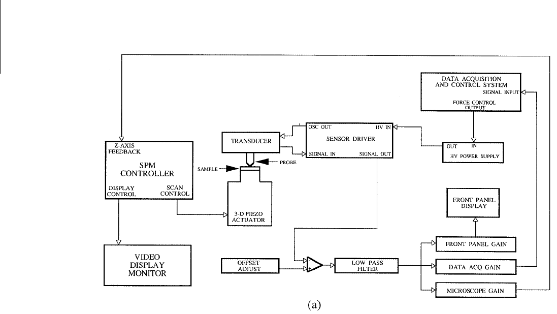
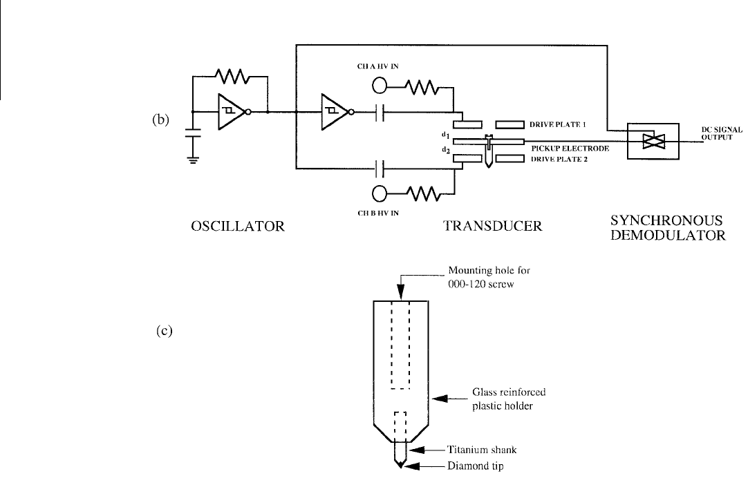
7.2.2 Nano/Picoindenter
As stated earlier, conventional AFMs have been used for indentation studies on nanometer-scale depths.
In these studies, the hardness value is based on the projected residual area after imaging the indent.
Direct imaging of the indent allows one to quantify piling up of ductile material around the indenter.
However, it becomes difficult to identify the boundary of the indentation mark with great accuracy. This
makes the direct measurement of the contact area somewhat inaccurate (Bhushan et al., 1994a,d). A
technique with the dual capability of depth sensing as well as
in situ
imaging is most appropriate in
nanomechanical property studies (Bhushan et al., 1996). This indentation system is used to make load-
displacement measurement and subsequently carry out
in situ
imaging of the indent. A schematic of the
nano/picoindenter system used is shown in Figure 7.1. The indentation system consists of a three-plate
transducer with electrostatic actuation hardware used for direct application of normal load and a capac-
itive sensor used for measurement of vertical displacement. The AFM head is replaced with this transducer
assembly while the specimen is mounted on the piezoelectric scanner which remains stationary during
indentation experiments. The transducer consists of a three (Be–Cu) plate capacitive structure which
provides high sensitivity, large dynamic range, and a linear output signal with respect to load or dis-
placement. The tip is mounted on the center plate. The upper and lower plates serve as drive electrodes.
Load is applied by applying appropriate voltage to the drive electrodes, thereby generating an electrostatic
force between the center plate and the drive electrodes. Vertical displacement of the tip (indentation
depth) is measured by measuring the displacement of the center plate relative to the two outer electrodes
using capacitance technique. The load resolution is 100 nN or better, and the displacement resolution is
0.1 nm. At present, a load range of 1 µN to 10 mN can be employed. Loading rates can be varied by
changing the load/unload period. The AFM functions as the platform providing an
in situ
image of the
indent with a lateral resolution of 1 nm and a vertical resolution of 0.2 nm. The load–displacement data

© 1999 by CRC Press LLC
can be acquired and displayed on the display monitor. Hardness value can be obtained from the load–dis-
placement data, as well as from direct measurement of the projected residual area of the indent after
imaging. Young’s modulus of elasticity is obtained from the slope of the unloading curve.
A three-sided Berkovich indenter with tip radius of about 100 nm is generally used for the measure-
ments, see Chapter 10 on Nanomechanical Properties in this book. Sharper diamond tips with included
angle of 60 to 90° and tip radii of 30 to 60 nm are sometimes employed for shallower indentation (on
the order of 1 nm). To obtain an accurate relation between the indentation depth and the projected
contact area, tip shape calibration needs to be done. Also for surfaces with rms roughness on the order
of indentation depth, the original (unindented) profile is subtracted from the indented profile (Bhushan
et al., 1994a,d).
In a typical indentation experiment, the tip is lowered close to the sample (ideally <100 µm). Scan
size and scan rate are selected. The tip is engaged to the sample surface by a stepper motor with a set
point of 1 nA (about 1 µN). A desired image area is captured prior to indentation. The feedback is set
to zero to disable the scanner; the scan size is set to zero so that the indenter will be positioned at the
center of the image. An appropriate set point for the preload condition is selected. The indentation rate
can be varied by changing the load/unload period.
7.3 Microscratching/Microwear Studies
By using a standard or sharp diamond tip mounted on a stiff cantilever beam, AFMs can be used to
investigate how surface materials can be moved or removed on micro- to nanoscales, for example, in
scratching and wear (where these things are undesirable) and nanofabrication/nanomachining (where
they are desirable) (Hamada and Kaneko, 1992; Miyamoto et al., 1991; Bhushan and Koinkar, 1994b,
1995a–c,e, 1997; Bhushan et al., 1994 a,c; 1995d; Bhushan, 1995a,b, 1997, 1998a,b; Koinkar and Bhushan,
1997a,b). A variety of polymers and ceramics and hard coatings have been studied. Many examples of
scratching/wear of magnetic recording materials have been presented in Chapter 14 on magnetic storage
devices in this book. This chapter focuses on the studies with silicon material.
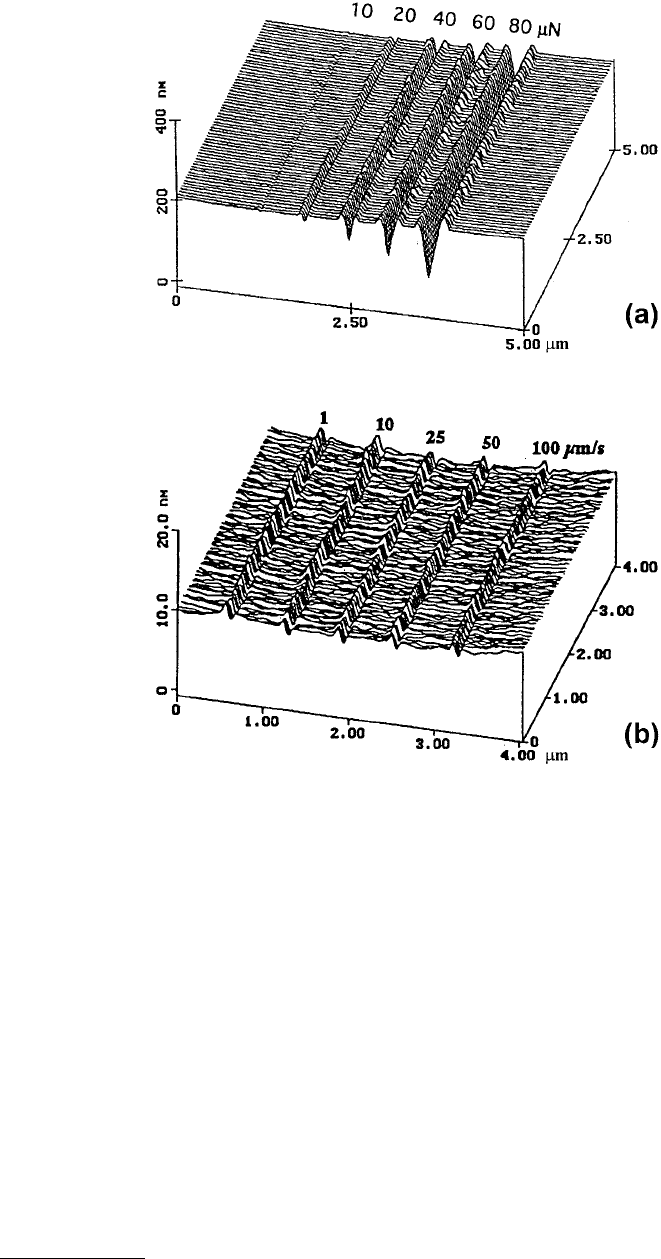
Figure 7.2a shows microscratches made on Si(111) at various loads (Bhushan and Koinkar, 1994b).
As expected, the scratch depth increases linearly with load. Such microscratching measurements can be
used to study failure mechanisms on the microscale and to evaluate the mechanical integrity (scratch
resistance) of ultrathin films at low loads. To study the effect of scanning velocity, unidirectional scratches,
5 µm in length, were generated at scanning velocities ranging from 1 to 100 µm/s at normal loads ranging
from 40 to 140 µN. There is no effect of scanning velocity obtained at a given normal load. For repre-
sentative scratches profiles at 80 µN, see Figure 7.2b (Koinkar, 1997). Insensitivity to scanning velocity
may be because of a small effect of frictional heating with the change in scanning velocity used here.
Furthermore, for a small change in interface temperature, there is a large underlying volume to dissipate
the heat generated during scratching (Bhushan, 1998a).
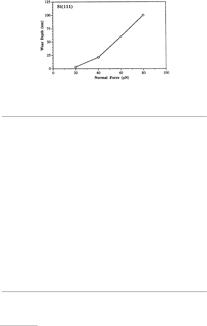
By scanning the sample in two dimensions with the AFM, wear scars are generated on the surface.
Figure 7.3 shows the effect of normal load on the wear rate. We note that wear rate is very small below
20 µN of normal load. A normal load of 20 µN corresponds to contact stresses comparable to the hardness
of the silicon. Primarily, elastic deformation at loads below 20 µN is responsible for low wear (Bhushan
et al., 1995d; Bhushan and Kulkarni, 1995f; Koinkar and Bhushan, 1997b).
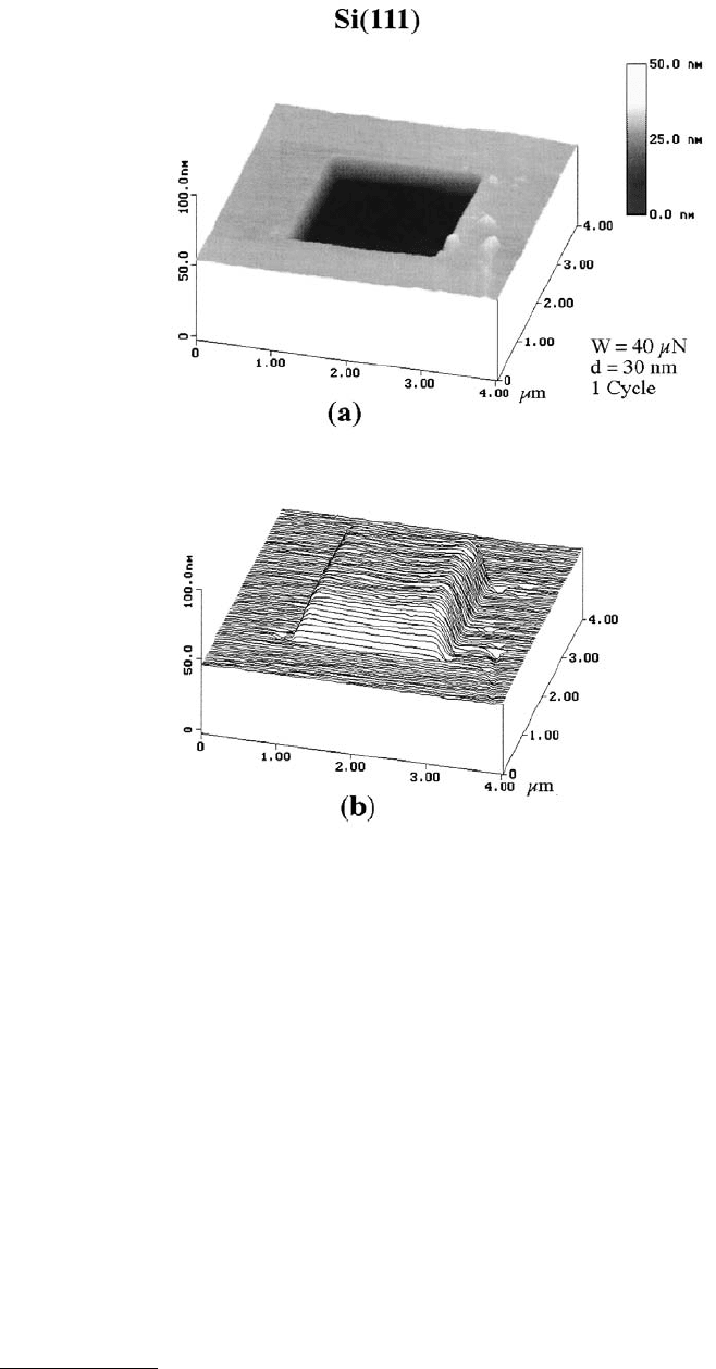
Typical wear mark generated at a normal load of 40 µN for one scan cycle and imaged using AFM at
300 nN load is shown in Figure 7.4a (Koinkar and Bhushan, 1997b). The inverted map of a wear mark
shown in Figure 7.4b indicates the uniform material removal at the bottom of the wear mark. Next we
examine the mechanism of material removal on microscale at low loads, in AFM wear experiments.
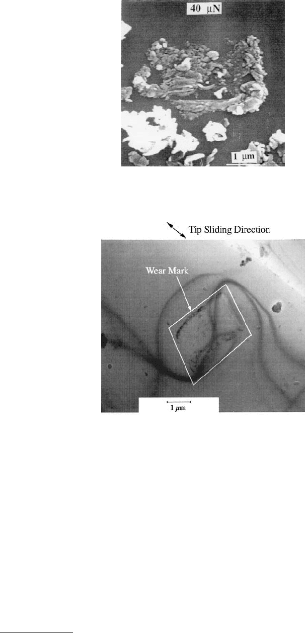
Figure 7.5 shows a secondary electron image of a wear mark and associated wear particles. The specimen
used for the SEM was not scanned after initial wear, to retain wear debris in the wear region. Wear debris
is clearly observed. An AFM image of the wear mark shows small debris at the edges, swiped during AFM
scanning. Thus, the debris is “loose” (not sticky) and can be removed during the AFM scanning. SEM
micrographs show both cutting-type and ribbonlike debris. TEM studies were performed to understand
© 1999 by CRC Press LLC
FIGURE 7.1
Schematics of (a) indentation system, (b) three-plate transducer with electrostatic actuation hardware and capacitance
sensor, and (c) tip-holder mount assembly. (From Bhushan, B. et al. (1996).
Philos. Mag.,
74, 117–1128
.
With permission.)
© 1999 by CRC Press LLC
FIGURE 7.1
© 1999 by CRC Press LLC
the material removal process. The TEM micrograph of the worn region in Figure 7.6 shows evidence of
bend contours passing through the wear mark. The bend contours around and inside the wear mark
suggest that there are some residual stresses around and inside the wear mark region. There is no
dislocation activity or cracks observed inside the wear track. The dislocation activity and/or cracking
probably occurs at the subsurface. Based on SEM and TEM studies, it is believed that the material in the
experiment described here is removed in a brittle manner without much plastic deformation (dislocation
activity).
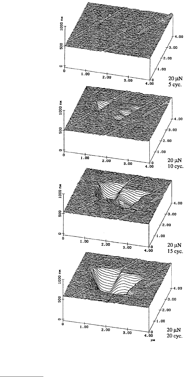
Finally, we study evolution of wear of a diamondlike carbon (DLC) coated disk substrate, Figure 7.7
(Bhushan et al., 1994a). The data illustrate how the microwear profile for a load of 20 µN develops as a
function of the number of scanning cycles. Wear is not uniform, but is initiated at the nanoscratches
indicating that the nanoscratches (with high surface energy) and nonuniform coverage of DLC at nano-
scratches act as initiation sites. Thus, scratch-free surfaces will be relatively resistant to wear.
FIGURE 7.2
Surface plots of (a) Si(111) scratched for ten cycles at various loads and a scanning velocity of 2 µm/s
(note that the
x
- and
y
-axes are in µm and the
z
-axis is in nm), and (b) Si(100) scratched in one unidirectional scan
cycle at a normal load of 80 µN and different scanning velocities.
© 1999 by CRC Press LLC
7.4 Nanofabrication/Nanomachining Studies
Scanning tunneling microscopes (STMs) have been used to form nanofeatures by localized heating or
by inducing chemical reactions under the STM tip (Abraham et al., 1986; Silver et al., 1987; Albrecht
et al., 1989; Utsugi, 1990; Kobayashi et al., 1993), and nanomachining (Parkinson, 1990). AFMs have also
been used for nanofabrication (Majumdar et al., 1992; Bhushan et al., 1994a,c; Bhushan, 1995a,b, 1998a,b;
Tsau et al., 1994) and nanomachining (Delawski and Parkinson, 1992).
Figure 7.8 shows an example of nanofabrication. The word “OHIO” was written on a (100) single-
crystal silicon wafer by scratching the sample surface with a diamond tip at specified locations and
scratching angles (Bhushan, 1995a). The normal load used for scratching (writing) was 50 µN and the
writing speed was 0.2 µm/s. Each line is scribed manually and debris at the ends of each line is visible.
A few lines are not connected to each other because of the PZT drift and hysteresis. Sufficient time should
be given for the thermal stabilization of the PZT scanner so that the hysteresis effect is small during the
nanofabrication. Next, more complex patterns were generated at a normal load of 15 µN and a writing
speed of 0.5 µm/s, Figure 7.9 (Koinkar, 1997). Such a type of patterns is useful for resistor trimming (to
increase the path resistor) on a small scale. The separation between lines is about 50 nm. In Figure 7.9a,
the variation in line width is due to the tip asymmetry. A spiral pattern generated as shown in Figure 7.9b.
Nanofabrication parameters — normal load, scanning speed, and tip geometry — can be controlled
precisely to control depth and length of the devices.
Nanofabrication using mechanical scratching has several advantages over other techniques (Koinkar,
1997). Better control over the applied normal load, scan size, and scanning speed can be used for
nanofabrication of devices. Using this technique, nanofabrication can be performed on any engineering
surface. Use of chemical etching or reactions is not required, and this dry nanofabrication process can
be used where use of chemicals and electric field is prohibited. One disadvantage of this technique is the
formation of debris during scratching. At light loads, debris formation is not a problem compared with
high-load scratching. However, debris can be removed easily out of the scan area at light loads during
scanning.
7.5 Nano/Picoindentation
Nanohardness measurements using conventional AFMs is covered in Chapter 14 on magnetic storage
devices. In this chapter, we will limit the discussion to the application of the three-plate transducer with
FIGURE 7.3
Wear depth as a function of normal load for Si(111) after one cycle. (From Koinkar, V. N. and Bhushan,
B. (1997),
J. Mater. Res.,
12, 3219–3224. With permission.)
© 1999 by CRC Press LLC
electrostatic actuation hardware used in conjunction with conventional AFMs (Bhushan et al., 1996;
Kulkarni et al., 1996a,b, 1997; Bhushan, 1997, 1998a,b; Bhushan and Koinkar, 1997; and Koinkar and
Bhushan, 1997a).
Figure 7.10a shows the load–displacement curves at different peak loads for Si(100). Load–displace-
ment data at residual depth as low as about 1 nm can be obtained. Loading/unloading curves are not
smooth, but exhibit sharp discontinuities particularly at high loads (shown by arrows in the figure). Any
discontinuities in the loading part of the curve probably result from slip of the tip. The sharp disconti-
nuities in the unloading part of the curves are believed to be due to formation of lateral cracks that form
at the base of median crack, which results in the surface of the specimen being thrust upward. From the
load–displacement curves in Figure 7.10 the indentation hardness of surface films with an indentation
depth of as small as about 1 nm has been measured. Triangular indentations are observed for shallow
penetration depths, Figure 7.10b.
FIGURE 7.4
(a) Typical gray scale and (b) inverted AFM images of a wear mark created using a diamond tip at a
normal load of 40 µN and one scan cycle on Si(111) surface. (From Koinkar, V. N. and Bhushan, B. (1997),
J. Mater.
Res.,
12, 3219–3224. With permission.)
© 1999 by CRC Press LLC
Figure 7.11 shows the load–displacement curves during three loading and unloading cycles for single-
crystal silicon. The unloading and reloading curves reveal a large hysteresis, which shows no sign of
degeneration through three cycles of deformation and the peak load displacement shift to higher values
in successive loading–unloading cycles. Pharr et al. (1989, 1990), Page et al. (1992), and Pharr (1992)
have also observed hysteresis behavior in silicon at similar loads using a nanoindenter. The fact that the
curves are highly hysteretic implies that deformation is not entirely elastic. Pharr (1992) concluded that
large hysteresis is due to a pressure-induced phase transformation from its normal diamond cubic form
to a
β
-tin metal phase.
Table 7.1 summarizes the hardness and Young’s modulus of eleasticity data at various depths for single-
crystal silicon (Bhushan et al., 1996). Comparison of nanohardness values with that of bulk hardness
FIGURE 7.5
Secondary electron image of wear mark and debris for Si(111) produced at a normal load of 40 µN
and one scan cycle. (From Koinkar, V. N. and Bhushan, B. (1997),
J. Mater. Res.,
12, 3219–3224. With permission.)
FIGURE 7.6
Bright-field TEM micrograph showing wear mark and bend contour around and inside the wear mark
in Si(111) produced at a normal load of 40 µN and one scan cycle. (From Koinkar, V. N. and Bhushan, B. (1997),
J. Mater. Res.,
12, 3219–3224. With permission.)
© 1999 by CRC Press LLC
FIGURE 7.7
Surface plots of DLC-coated thin-film disk showing the worn region; the normal load and number of test
cycles are indicated. (Bhushan, B. et al. (1994),
Proc. Inst. Mech. Eng. Part J: J. Eng. Tribol.
208, 17–29. With permission.)